
Advanced artificial synaptic thin-film transistor based on doped potassium ions for neuromorphic computing via third-generation neural network†
Yixin
Cao‡
a,
Tianshi
Zhao‡
 a,
Chun
Zhao
*ab,
Yina
Liu
cd,
Pengfei
Song
ab,
Hao
Gao
e and
Ce Zhou
Zhao
ab
a,
Chun
Zhao
*ab,
Yina
Liu
cd,
Pengfei
Song
ab,
Hao
Gao
e and
Ce Zhou
Zhao
ab
aDepartment of Electrical Engineering and Electronics, University of Liverpool, Liverpool L69 3GJ, UK. E-mail: Chun.Zhao@xjtlu.edu.cn
bSchool of Advanced Technology, Xi’an Jiaotong-Liverpool University, Suzhou 215123, China
cDepartment of Applied Mathematics, Xi’an Jiaotong-Liverpool University, Suzhou 215123, China
dDepartment of Applied Mathematics, University of Liverpool, Liverpool L69 7ZD, UK
eEindhoven University of Technology, Eindhoven, The Netherland
First published on 26th January 2022
Abstract
As the basic and essential unit of neuromorphic computing systems, artificial synaptic devices have great potential to accelerate high-performance parallel computation, artificial intelligence, and adaptive learning. Among the proposed artificial synaptic devices, the synaptic transistors are well considered to be one of the most suitable devices for simulating artificial intelligence. So far, synaptic transistors based on iontronic have been proposed and proved to demonstrate great potential in artificial intelligence applications. However, little research specifically focused on improving the device's ability to mimic synaptic behaviour. Here, we proposed the enhancement of synaptic properties of the solution-based thin-film transistors based on potassium ion conduction in the dielectric layer for the first time. Due to the formation of a gated electrical double-layer, the transistor exhibited an enlarged memory window. Based on this, the excitatory postsynaptic current in the synaptic thin-film transistor was modified accordingly, which further enhanced the suitability of the proposed synaptic thin-film transistor for simulating biological synapses. In addition, considerable synaptic properties were evaluated elaborately, including paired-pulse facilitation, short-term memory, long-term memory, and spike-time-dependent-plasticity. Most importantly, according to the impressive results of the Artificial Neural Network algorithm's image recognition simulation, the simulation image recognition rate based on the mentioned artificial synaptic devices reached as high as 92%. Last but not least, in order to simulate biological neurobehavior more closely, the Spiking Neural Network algorithm was also successfully implemented to complete the specified machine learning task, which further proved the great potential of the synaptic devices in advanced low-power neural network systems.
Introduction
With the increase in the amount of data and demand for parallel computing, modern computers based on the von Neumann architecture are facing severe challenges of inefficient information processing.1–3 Inspired by biological neural network systems, massively parallel neuromorphic computing was then proposed accordingly.2,4 Unlike the traditional logic circuit with transistors connected by only one or less than a handful of other components, one neuron in the neural network could connect to a thousand other neurons.2 Since information processing can be highly parallel within a dense neural network, the data selection characteristics of neural networks are considered to be more power-efficient for artificial intelligence than the existing von Neumann computing architecture.5–8 The basic and essential unit in a neural network is the synapse, which is regarded as the functional connection between two adjacent neurons in the biological brain.9 The strength of the synapse, i.e., the synapse weight, could be adjusted and memorized, through which the neuron can transfer and analyze the information.7,9,10 Therefore, the development of artificial synaptic devices towards an artificial neural network to mimic similar functions of the biological neural network is greatly worthy of investigation. Over the past decades, significant efforts have been extensively devoted to developing a synaptic device to trigger synaptic plasticity and non-volatility. In order to mimic and simulate synaptic activity, typically, the two-terminal memristors with reversible analogue switch behavior such as oxide-based resistance random access memory (RRAM),11,12 ferroelectric memory,13,14 and phase-change memory (PCM)15,16 were well studied and reported. Nevertheless, it is considered to be a significant obstacle for them to enable both learning and signal transmission simultaneously.17 In addition, the reduced control of conductance changes and asynchronous read/write operations limits the further application of two-terminal memristor devices as synaptic elements. Although several solution schemes based on consecutive update-verify procedures have been initiated and attempted to modify the weight adjusting procedure of synaptic devices,3 they further induced energy-expensive and device-to-device access, and increased the complexity of peripheral circuit design from application perspectives. Consequently, the energy-saving advantages of neuromorphic computing in data processing will no longer hence exist.18–21To overcome these mentioned challenges, synaptic transistors have been proposed accordingly, such as ferroelectric-gate synaptic transistors and electrolyte-gate synaptic transistors.9,14,22,23 Compared with two-terminal memristor devices, the synaptic transistor with individually controllable three terminals can effectively prevent crosstalk between adjacent devices, allowing selective and parallel weight update.24 In addition, the channel conductance between the source (S) and the drain (D) electrodes of the synaptic transistor-like devices could be adjusted by the gate (G) voltage, which is recognized as synapse weight.10 Therefore, neuromorphic computing is widely considered to be realized with a broad application prospect via three-terminal synaptic transistors. Recently, the mechanism for devices to possess synaptic properties has been proposed tentatively, such as electrostatic modulation, iontronic theory, and ferroelectric effect theory.2,14,25–28 Moreover, many kinds of research are worth discussing on how to optimize the mechanism of synaptic devices. At the same time, it is worthwhile to study the mechanism of the synaptic transistors from the perspective of material characterization. In addition, diverse research of neuromorphic applications still relies on traditional algorithms that have a weight updating process different from the real biological neuron system, such as ANN. Therefore, simulating biological neural networks more realistically in neural networks is of significant worth studying.
Here we propose a novel technology of doping potassium (K+) ions in the dielectric layers to enhance the synaptic characteristics of solution-processed synaptic thin-film transistors (TFT) for the first time. For biological individuals, as an indispensable element in the human body, K+ ions play an important role in nerve signal transmission.23 For a gated transistor-like device, the K+ in ion conducted dielectric contributes to the formation of the electric double-layer (EDL) at the interface between the dielectric and semiconductor layer, which leads to an increase of the controllable and repeatable memory window.2 As a result, the transmission characteristic curve of the synaptic transistor will be more adaptable to mimic the synaptic activity. In addition, due to the effects of electrostatic modulation and electrochemical doping, devices doped by K+ ions have greater relaxation time, causing the artificial synaptic transistor similar to the real biological synapse. For the proposed synaptic transistor, the indium oxide (InOx) and alumina (AlOx) were served as the n-type channel and dielectric materials, respectively. Both AlOx and InOx thin films were prepared by solution method, which is well proved to have low cost and high composition controllability.29 The synaptic plasticity was then simulated, such as paired-pulse facilitation (PPF), short-term memory (STM), long-term memory (LTM), spike-time-dependent-plasticity (STDP). Furthermore, the image recognition process was simulated using Artificial Neural Network (ANN) and Spiking Neural Network (SNN) algorithms. The simulated image recognition rate by ANN algorithms after 20 learning epochs reached 92%, which is close to the theoretical value that the learning rate is 1 (96%). In addition, although ANN's deep learning model has proven its powerful learning capabilities, it requires expensive computing resources and significant power consumption, making it difficult to be applied on the mobile edge devices such as smartphones and watches.30 Furthermore, ANN employs a “classical” backward propagation approach in order to demonstrate classification. The backward propagation has no relation with neuromorphic computing as it only utilizes the static weight of the synapses (G+ − G−) but not their complex temporal properties. Therefore, the SNN algorithm, another advanced neuromorphic calculation model for the 3rd generation neural network with significant energy efficiency, has been proposed. Being an artificial neural network constructed using knowledge observed in biology, SNN uses spatiotemporal information (such as STDP) to update synaptic weights based on local learning rules,31 in which neurons connect neurons through synapses with adjustable weight values. Moreover, some recent study suggests that the STDP learning rule is involved in the formation of associative memory.32 Therefore, SNN is capable of more closely mimicking the working mode of biological synapses. In this work, the Mixed National Institute of Standards and Technology (MNIST) data set was also successfully identified under the SNN algorithm and well proved to obtain extremely low energy consumption.
Experimental section
For the solution preparation, the AlOx precursor solution with a concentration of 2.5 M was prepared by dissolving aluminium nitrate nonahydrate (Al(NO3)3·9H2O, Aladdin) in deionized water (DI water). Based on the K+ doping concentration, the 0, 1, and 10 at% K+ ion-doped AlOx precursors were prepared by adding 0, 0.025, and 0.25 M potassium chloride (KCl, 99.99% metals basis, Aladdin) into the AlOx precursor solution, respectively. The InOx precursor solution with a concentration of 0.15 M was prepared by dissolving indium nitrate hydrate (In(NO3)3·xH2O, Aladdin) in deionized water (DI water). Subsequently, the prepared precursor solutions were ultra-sonicated and filtered through a 0.45 μm poly (ether sulfone) (PES) syringe to obtain transparent solutions.For TFTs fabrication, the heavily doped n-type silicon (n++ Si) was utilized as the gate substrate. In order to prepare the dielectric layer, the AlOx precursor solution with and without specific K+ ion doping were spun onto the plasma-treated n++ Si substrate and then annealed at 300 °C under ambient atmosphere for 30 minutes. After that, the InOx precursor solution was spun onto the surface of the dielectric layer and then annealed at 250 °C for 30 minutes in an ambient atmosphere. Finally, the Al source and drain electrodes were deposited onto the semiconductor layer through thermal evaporation. The channel length (L) and width (W) were 10 and 150 μm, respectively, with a thickness of 100 nm.
The surface roughness of the K+ doped AlOx layers was observed by atomic force microscopy (AFM, Bruker Nanoscope V). The surface morphology of the AlOx layers was characterized by using a scanning electron microscope (SEM, Hitachi S4700). The element distribution of the sample was characterized by using the energy-dispersive X-ray spectroscopy (EDS, Hitachi S4700). The chemical bonds were measured through X-ray Photoemission Spectroscopy (XPS, Thermo scientific ESCALAB 250Xi with Al Ka X-ray source). The electrical characteristics and synaptic characteristics test of the TFTs were revealed utilizing a semiconductor analyzer (Keysight, B1500 A) in the dark condition at room temperature.
Results and discussion
Generally, as depicted in Fig. 1a, for biological individuals, signals are transmitted from presynaptic neuron to postsynaptic neuron through synapses in nervous systems.33 When presynaptic neurons receive external stimuli, ions in the extracellular fluid enter synaptic neurons through ion conduction and form memory by generating graded potentials and action potentials.34 In order to mimic the behaviour of biological synapses, the electrochemical artificial synaptic TFTs based on K+ doped AlOx dielectric and InOx semiconductor were fabricated as described in Fig. 1a. For these devices, the Al gate electrode, InOx semiconductor, and K+ ions represent the presynaptic neuron, the postsynaptic neuron, and neurotransmitter, respectively. Fig. 1b shows the transfer characteristic curves of the TFTs with or without K+ ions doped AlOx dielectric layer, indicating typical characteristics of n-type TFTs. According to the results, under the gate voltage (VG) swept forward and backwards from −2 to 4 V, the devices with K+ doped AlOx dielectric exhibit an obvious counter-clockwise hysteresis window than the ones without K+ doping. This could be utilized as the basis for the synaptic properties of the devices. In addition, from the distribution diagram in Fig. S1 (ESI†), it could be concluded that the device memory window in this work shows the normal distribution. In order to further investigate the surface morphology of the thin films, the AFM measurement was then operated, and the result is shown in Fig. 1c. The root-mean-square (RMS) roughness value of the AlOx film without K+ ions is 0.138 nm, while the AlOx film doped by K+ ions is 0.202 nm. This phenomenon shows that doping did not deteriorate the surface roughness of AlOx, and all the deposited films are of nanoscale smoothness which is beneficial for fabricating a high-quality channel layer and advantageous for obtaining TFT with high stability.35,36 The SEM image in Fig. 1d also indicates that the produced K+ doped AlOx film exhibits flat and dense properties. The element map scanning during the EDS analysis was operated accordingly, and the results are shown in Fig. 1e to Fig. 1g. It is worth noting that Fig. 1f demonstrates that the doped K+ ions are evenly distributed in the film. | ||
| Fig. 1 (a) Schematic diagram of the K+ doped AlOx synaptic TFT. (b) Transmission characteristics of AlOx with and without K+ doped. (c) AFM images of AlOx with and without K+ doped. (d) SEM image of surface topography in AlOx surface view. The EDS mapping of (e) N, (f) K, (g) O elements in AlOx coating on Si substrate. (h) K+ ions migration in the K+ doped AlOx solid-state electron by bias spikes. (i) XPS image of the surface InOx film. | ||
In the biological neuron network, information transmission is mainly in the form of a bioelectrical pulse. The nerve fibres of each neuron are not directly connected but separated by other substances. When a bias input reaches the end of presynaptic neurons, basic ion neurotransmitters are released into synapses, resulting in new electrical bias spikes on adjacent postsynaptic neurons.36 Similarly, for artificial synaptic TFT, the mobile K+ ions in the AlOx dielectric act as neurotransmitters, resulting in the changing of the channel conductance. The mechanism of channel conduction modulation is proposed in Fig. 1h. When the positive electric spike is applied to the gate of the synaptic TFT, the moving K+ ions will drift toward the dielectric/semiconductor interface.37 These migrated K+ ions could modulate the channel conductance through two types of iontronic modulation processes: EDL modulation (under weak bias peak) and electrochemical doping (under strong bias voltage).25,37 For EDL modulation, the migrated K+ ions will accumulate at the dielectric/semiconductor interface, inducing the accumulation of channel electrons.38,39 Consequently, the channel conductance will increase. Once the external electric field is removed, K+ ions will diffuse back to their original equivalent position due to the concentration gradient within a short period of time, and the EDL will then disappear. For electrochemical doping, other than the EDL modulation, part of the migrated K+ ions will penetrate the InOx channel, causing the increase of the channel conductance.40 After the removal of the gate voltage, the penetrated K+ ions will gradually diffuse back to the original equivalent position, and this process will take a long period of time, leading to long-term retention of the increased channel conductance.25–27 As mentioned above, the mobile K+ ions within K+ doped AlOx dielectric contribute to the formation of an EDL and electrochemical doping, resulting in short-term retention and long-term retention, respectively.23,41–43 To prove the existence of the EDL, the metal-insulated semiconductor structure device was fabricated (Fig. S2, ESI†). Moreover, the capacitance–voltage (C–V) and capacitance-frequency (C–F) were tested. Fig. S3a (ESI†) shows the C–V test result, in which the gate voltage increases from −2 to 4 V and the capacitance of the device increases from 1.6 × 10⁻⁷ to 5.3 × 10⁻⁷ F cm−2. During the artificial synaptic TFT operation, these specific capacitances are maintained at a high level. Compared with the control group without K+ doping, the capacitance increased significantly, considering K+ and protons in K+ doped AlOx strongly accumulate on the InOx/K+ doped AlOx interface to form EDL under the action of an electric field, which can be regarded as a nanogap capacitor with ultra-high capacitance, thereby increasing the capacitance.38 Fig. S3b (ESI†) illustrates the C–F test result. The specific capacitance distribution can be divided into two areas, the high-frequency area with a small capacitance value (>10 kHz) and the low-frequency area with a large capacitance value (<10 kHz)). The one in the high-frequency region (>10 kHz) refers to a bulk electrolyte capacitance with a fast-charging speed. The increase in capacitance in the low-frequency region (<10 kHz) is reasonably related to the formation of an EDL at the InOx/K+ doped AlOx interface. The EDL obtains large capacitance through the migration and accumulation of ions on the interface.25,37 Furthermore, the C–V relationship at several frequencies was tested, and the results are shown in Fig. S3c (ESI†). At 10 kHz–1 MHz, the capacitance exhibits a weak Vgs dependence. At 1 kHz, with the increase of Vgs, the capacitance increases significantly, indicating the presence of pseudocapacitance. Through the integration of the C–V curve, the total accumulated charge QT can be found:43
In synaptic TFT, the excitatory postsynaptic current (EPSC) is used to manifest the channel conductance and indicate the response to presynaptic signals, i.e., the gate bias (Fig. 2a).45 When the gate bias is applied in the form of pulses, the EPSC in the synaptic TFT could show a modulated trend that effectively mimics the excitability changes in biological neurons (synaptic plasticity). As shown in Fig. S5 (ESI†), a positive gate pulse could cause an immediate increase of EPSC followed by a gradual recovery, while a negative gate pulse leads to an opposite response. Most importantly, the EPSC can be arbitrarily regulated, which is the research basis of synaptic devices.42,46,47 In the neuromorphological system, neurofacilitation, also named paired-pulse facilitation (PPF), is known as typical synaptic behaviour.48 Due to the memory effect, if two presynaptic peaks are close enough, the EPSC peak resulting from the first presynaptic peak cannot be eliminated entirely, and the peak generated by the second presynaptic peak will be enhanced accordingly.48,49 A pair of presynaptic spikes (4 V, 30 ms) with a pulse interval (Δt) of 20 ms was continuously applied to the gate, as shown in Fig. 2b. The second EPSC peak triggered by presynaptic pulses is much higher than that of the first. Fig. 2c depicts the PPF index as a function of the interval time between pairs of pulses. The PPF index curve can be fitted as follows double-phase exponential function:50
| PPF index = A2/A1 = 1 + C1 exp (−Δt/τ1) + C2 exp (−Δt/τ2) |
| E = Vds × Ids × t |
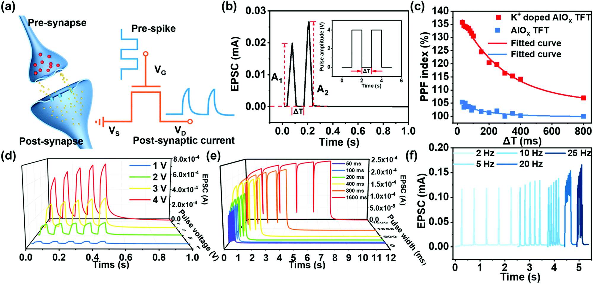 | ||
| Fig. 2 (a) The principle of signal transmission from pre-synaptic to post-synaptic in biological synapses and simulation of the electrical impulse of artificial synaptic TFT. (b) Two consecutive presynaptic spikes (4 V, 30 ms) generate EPSC. Interval time (Δt) is 100 ms. (c) The PPF index is defined as the function of the ratio of A2/A1 and two pulses (4 V, 30 ms) interspike interval (Vds = 4 V). (d) EPSC is generated by five presynaptic spikes (1 V to 4 V, 50 ms), Δt is 50 ms (Vds = 2 V). (e) The enhancement effect of five consecutive presynaptic pulses (2 V) on EPSC, the pulse time varies from 50 ms to 1600 ms (Vds = 2 V). (f) EPSC (Vds = 4 V) is generated by five presynaptic spikes (4 V, 30 ms) with different pulse frequencies (2 Hz–25 Hz). | ||
The multi-storage model proposed by Atkinson and Shiffrin (as demonstrated in Fig. 3a) shows that human memory has three components: sensory memory, STM, and LTM.66 The external environment input of new information is firstly stored in the sensory register as a sensor memory in a short period and then selectively converted to temporary STM in short-term memory storage or permanent LTM in long-term memory storage. If the sensory stimuli are repeated frequently, STM will be transformed into LTM. Due to the complexity of the neural processes known to be realized in neural engineering, it is difficult to prove that neural processes are interconnected. However, the TFTs can simulate the synaptic function of STM and LTM characteristics by using input repetitive pulse stimulation. As shown in Fig. 3b, a series of electrical pulses (number of 5, 10, 20, 50, 100, 200) with a fixed duration of 100 ms and a voltage intensity of 4 V was applied to the synaptic device. It shows that EPSC rises under a positive pulse, which can be regarded as “learning”. The learning state is defined as the state at the end of the positive pulse. When presynaptic spikes had finished, the synaptic weight decays spontaneously over time. This decay process is similar to the forgetting process of biological synapse behaviour. In Fig. 3c, with the increase of the number of learning pulses, the drop of EPSC as a function of time gradually slows down, indicating the transition from STM to LTM.3,49 In addition, due to the presence of electrochemical doping, the charge can be preserved for a long time. Furthermore, the learning process based on positive pulses is reversible, which means that the negative pulse input could accelerate the EPSC decrease process. Based on this, in addition to long-term potentiation (LTP), the device also exhibited long-term depression (LTD) characteristics. The LTP and LTD together formed the basis of neural computing. As shown in Fig. 3d, 50 positive voltage pulses were applied to enhance the synaptic weight (channel conductance, G) and simulate the “learning” function. Then 50 negative voltage pulses were applied to depress the synaptic weight and represent the “erasing” function.
 | ||
| Fig. 3 (a) The multi-storage model of human memory was proposed by Atkinson and Shiffrin. (b) EPSC is generated by different numbers (5–200 times) of presynaptic spikes (4 V, 80 ms), and EPSC is observed to be gradually increased. (c) As the number of applied pulses increases, it changes from STM to LTM. After different numbers (5–200 times) of presynaptic spikes stimulate 60 s, the current is still stored. (d) Conductance change during learning (by positive spike: 4 V, 100 ms) and erasing (by negative spikes: 2 V, 100 ms). | ||
In order to investigate the stability of the device, 25 mentioned full-scale “writing” and “erasing” cycles were tested in the device, as shown in Fig. 4a. The results show that the device's synaptic behaviour remains stable after 2500 pulses. Ideally, the linear proportions existed between the increase and decrease of G and the number of electrical pulses. In fact, the cumulative conductance is unable to exactly follow a simple linear correlation, which leads to non-linearity (NL) of the synaptic weight update. The value of G could be then described by function:3
| GP = BP[1 − exp (γP/AP)] + Gmin |
| GD = −BP[1 − exp(P − γ/AD)] + Gmax |
| BP/D = (Gmax − Gmin)/[1 − exp(−γ/AP/D)] |
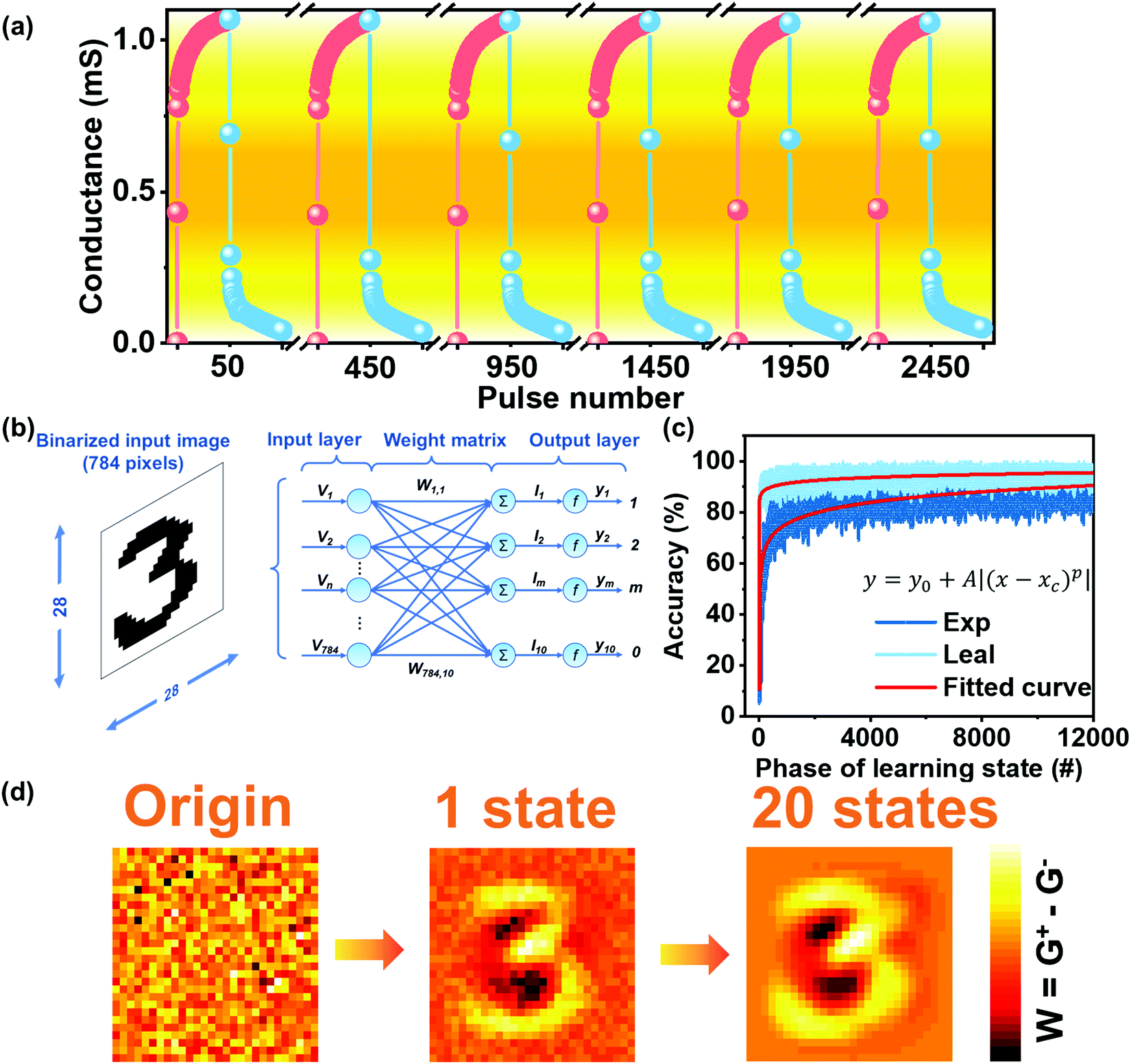 | ||
| Fig. 4 (a) Use 25-cycle pulses (50 positives (4 V) and 50 negatives (−2 V) pulses with a pulse duration of 50 ms and an interval of 50 ms) to simulate the synaptic TFT channel conductance. (b) ANN structure used in the simulation. (c) Simulation of MNIST digit recognition accuracy based on synaptic TFT perceptron neural network. (d) Mapping images of test data sets for three different learning epochs. | ||
To further explore the neuromorphic computational simulation capabilities of K+ doped AlOx TFT synaptic devices, a handwritten artificial neural network was developed, which can simulate the numbers in the revised MNIST data set through the ANN algorithm.3,68 Specifically, as shown in Fig. 4b, since the synapse layer is composed of 28 × 28 input neurons, the input pattern contains the same number of pixels, which are fully connected with 7840 synaptic weights and converted into 10 output neurons. It is worth noting that the synaptic TFTs have only positive channel conductance, while there are positive conductance and negative conductance in the weight matrix. Therefore, the conductance difference between two equivalents synaptic structures was defined as the synapse weight, which can be expressed as W = G+ − G−. Here, the symbol W represents the synapse weight. Based on the backpropagation algorithm, W increases as G+ increases and decreases as G− increases. As described in Fig. 3d, the G of the device can be increased by applying a positive voltage pulse, and the application of a negative pulse will cause the G of the device to decrease. The conductance change extracted from the “learning” and “erasing” curves describes the detailed information of the synaptic weight change. It can be concluded that the Gmax/Gmin ratio of the synaptic device is 25.1. According to previous literature, good linearity and a high Gmax/Gmin ratio will improve the final recognition accuracy.67,69 In the simulation, due to the high Gmax/Gmin ratio (25.1) and suitable linearity (NLP = 0.8884, NLD = 3.54), the recognition accuracy can reach 92% after 20 learning cycles, as shown in Fig. 4c. Moreover, the experimental device's recognition accuracy also approaches the ideal accuracy based on linear weight updating route and unlimited Gmax/Gmin (96% after 20 periods). As shown in Fig. 4d, considering the handwritten number “3” as an example, the output matrix was drawn in the mapped image (28 × 28 pixels). Initially, the output was random without any image information, and after 20 learning states, the shape of “3” became recognizable accordingly.
In addition, the SNN algorithm-based simulation for image recognition was further attempted. Compared with ANN, SNN is closer to the actual working model of biological synapses. As shown in Fig. 5a, the ANN algorithm is based on a continuous mathematically-defined nonlinear activation function. However, the information processing modes of the human brain and the artificial neural networks are distinguished from each other. Typically, the information is encoded as binary spikes in the human brain, while most artificial neural networks use real-valued vectors to represent data. As a comparison to ANN and shown in Fig. 5a, the SNN is all-or-none output in response to input spikes. It is also regarded as the “third-generation” neural network since it has the potential to replace deep learning methods in the fields of computational neuroscience and biological trusted machine learning.70 The binary (spike or no spike) operation is considered to be more suitable for fast and energy-efficient simulation on hardware devices.71 In addition, the SNN can emulate the human brain more faithfully on artificial neuromorphic hardware due to its noise resiliency, energy efficiency, and convenient implementation.72 The shaping of weight is based on the following two rules: Firstly, any synapses that contribute to the firing of postsynaptic neurons should become stronger, and their value should increase; Secondly, the synapse that does not contribute to the firing of the postsynaptic neuron should be weakened. Typically, as shown in Fig. 5b, multiple neurons are connected to a single neuron through synapses. Each presynaptic neuron fires at its own rate, and the spike is sent forward by the corresponding synapse. The strength of the spikes converted to postsynaptic neurons depends on the strength of the connecting synapses. Due to the input spike, the membrane potential of the postsynaptic neuron increases and emits a spike after crossing the threshold. When the postsynaptic neuron spikes, it will monitor which presynaptic neurons help it fire. This can be acquired by observing which presynaptic neurons spiked before the postsynaptic neurons spiked. Therefore, the postsynaptic spike is then induced by increasing the membrane potential, so the corresponding synapse is strengthened accordingly.
 | ||
| Fig. 5 (a) ANN algorithm and SNN algorithm function diagram. (b) SNN algorithm weight update diagram. (c) STDP response based on K+ doped AlOx synaptic devices. (d) Image recognition rate of SNN algorithm. (e) Different stage results of training the SNN using the MNIST data set. Via the generation characteristics of the SNN, the image is reconstructed using the training weights connected to each output neuron to view the learning situation of the network. | ||
In order to operate the SNN simulator, the STDP behaviour of the device served as the principle rule to update the weights and classify patterns, which is considered to be a biological process used by the brain to modify its neural connections. Fig. 5c shows the STDP curve of the synaptic device under electric pulse Vds of 1 V and Vgs of 1 V with both pulse duration of 30 ms. The STDP is the change in the synaptic weight (Δw) between pre-and postsynaptic spikes which can be modulated by using relative time duration between them.73 The Δw is defined as (GPost − GPre)/GPre, where GPre and GPost are conductance after the pre-and postsynaptic spikes, respectively. It could be observed that if the pre-spiking precedes the post-spiking (Δt >0), the connection strength of the synapse between two neurons would be reinforced. On the contrary, Δt <0 led to a depression phenomenon.
During the SNN simulation, the GPost weight used is the conductance of 1 s after Vpost or Vpre, and the maximum time interval Δt between Vpost and Vpre is 3.2 s during the process of testing STDP. To prove this simulation further closer to the actual hardware conditions, a time interval as an additional inference period was added. Therefore, the 4.3 s, which is slightly larger than the summation of Δt and one-second postpone, was chosen as an additional inference period. Fig. 5d shows the simulation result of image recognition using the SNN algorithm. The recognition rate of the MNIST data set after training reached 86%. Fig. 5e shows the weights of all synapses connected to a specific output neuron (the number is 400) after training based on the MNIST dataset. The red line in the figure represents the variable threshold. The threshold of each mode was calculated based on the number of contained activations. As shown in the inset diagram, the trained weight matrix could successfully recognize the image.
Conclusions
In summary, the solution-processed synaptic TFTs with K+ doping were fabricated and investigated. By doped K+ ions, the pristine InOx/AlOx TFTs exhibited enhanced synaptic behaviour. Based on the strong interfacial electric-double-layer coupling effect and electrochemical doping effect, the K+ doped transistors showed an obvious anti-clockwise memory window, which leads to a regulated EPSC behaviour. Moreover, several essential synaptic properties were measured, including PPF, STM, LTM, and STDP. Most importantly, under the simulation based on the ANN algorithm, the image recognition rate of the MNIST database for the proposed K+ doped device is as high as 92%. Based on the SNN algorithm, the image recognition task was also successfully simulated and proved its advantage in energy consumption. Overall, the TFTs experimental results present a simple and low-cost method to enhance the synaptic characteristics of artificial synaptic TFT, which is expected to act as a basic computing unit in the next generation of the neuromorphic system and has the potential to give birth to better robots, self-driving cars, medical diagnosis, and other intelligent human-computer interaction systems.Conflicts of interest
There are no conflicts to declare.Acknowledgements
This research was funded in part by the Natural Science Foundation of the Jiangsu Higher Education Institutions of China Program (19KJB510059), Natural Science Foundation of Jiangsu Province of China (BK20180242), the Suzhou Science and Technology Development Planning Project: Key Industrial Technology Innovation (SYG201924), University Research Development Fund (RDF-17-01-13), and the Key Program Special Fund in XJTLU (KSF-P-02, KSF-T-03, KSF-A-04, KSF-A-05, KSF-A-07, KSF-A-18).References
- J. Backus, Commun. ACM, 1978, 21, 613–641 CrossRef.
- S. Z. Bisri, S. Shimizu, M. Nakano and Y. Iwasa, Adv. Mater., 2017, 29, 1607054 CrossRef PubMed.
- R. Yu, E. Li, X. Wu, Y. Yan, W. He, L. He, J. Chen, H. Chen and T. Guo, ACS Appl. Mater. Interfaces, 2020, 12, 15446–15455 CrossRef CAS PubMed.
- D. Kuzum, S. Yu and H. S. Wong, Nanotechnology, 2013, 24, 382001 CrossRef PubMed.
- L. Abbott and W. G. J. N. Regehr, Nature, 2004, 431, 796–803 CrossRef CAS PubMed.
- D. Seok Jeong, I. Kim, M. Ziegler and H. Kohlstedt, RSC Adv., 2013, 3, 3169–3183 RSC.
- K. C. Kwon, Y. Zhang, L. Wang, W. Yu, X. Wang, I.-H. Park, H. S. Choi, T. Ma, Z. Zhu and B. Tian, ACS Nano, 2020, 7628–7638 CrossRef CAS PubMed.
- J. J. Harris, R. Jolivet and D. J. N. Attwell, Neuron, 2012, 75, 762–777 CrossRef CAS PubMed.
- B. Tang, S. Hussain, R. Xu, Z. Cheng, J. Liao and Q. Chen, ACS Appl. Mater. Interfaces, 2020, 12, 24920–24928 CrossRef CAS PubMed.
- Y. Liu, W. Yang, Y. Yan, X. Wu, X. Wang, Y. Zhou, Y. Hu, H. Chen and T. Guo, Nano Energy, 2020, 104930 CrossRef CAS.
- J. Park, M. Kwak, K. Moon, J. Woo, D. Lee and H. J. I. E. D. L. Hwang, IEEE Electron Device Lett., 2016, 37, 1559–1562 CAS.
- C. Y. Lin, J. Chen, P. H. Chen, T. C. Chang, Y. Wu, J. K. Eshraghian, J. Moon, S. Yoo, Y. H. Wang, W. C. Chen, Z. Y. Wang, H. C. Huang, Y. Li, X. Miao, W. D. Lu and S. M. Sze, Small, 2020, 16, e2003964 CrossRef PubMed.
- S. Boyn, J. Grollier, G. Lecerf, B. Xu, N. Locatelli, S. Fusil, S. Girod, C. Carrétéro, K. Garcia and S. J. N. C. Xavier, Nat. Commun., 2017, 8, 1–7 CrossRef PubMed.
- M.-K. Kim and J.-S. Lee, Nano Lett., 2019, 19, 2044–2050 CrossRef CAS PubMed.
- T. Tuma, A. Pantazi, M. Le Gallo, A. Sebastian and E. J. N. N. Eleftheriou, Nat. Nanotechnol., 2016, 11, 693 CrossRef CAS PubMed.
- Q. Wan, F. Zeng, J. Yin, Y. Sun, Y. Hu, J. Liu, Y. Wang, G. Li, D. Guo and F. J. N. Pan, Nanoscale, 2019, 11, 5684–5692 RSC.
- Y. Park, M.-K. Kim and J.-S. Lee, J. Mater. Chem. C, 2020, 8, 9163–9183 RSC.
- C. Li, D. Belkin, Y. Li, P. Yan, M. Hu, N. Ge, H. Jiang, E. Montgomery, P. Lin and Z. J. N. C. Wang, Nat. Commun., 2018, 9, 1–8 CrossRef PubMed.
- F. Alibart, L. Gao, B. D. Hoskins and D. B. J. N. Strukov, Nanotechnology, 2012, 23, 075201 CrossRef PubMed.
- L. Gao, F. Alibart and D. B. Strukov, 2012 IEEE/IFIP 20th International Conference on VLSI and System-on-Chip (VLSI-SoC): IEEE, 2012, pp. 88–93 Search PubMed.
- L. Gao, P.-Y. Chen and S. J. I. E. D. L. Yu, IEEE Electron Device Lett., 2015, 36, 1157–1159 Search PubMed.
- L. Q. Guo, H. Han, L. Q. Zhu, Y. B. Guo, F. Yu, Z. Y. Ren, H. Xiao, Z. Y. Ge and J. N. Ding, ACS Appl. Mater. Interfaces, 2019, 11, 28352–28358 CrossRef CAS PubMed.
- E.-K. Jang, Y. Park and J.-S. Lee, Nanoscale, 2019, 11, 15382–15388 RSC.
- S. Kim, Y. Lee, H.-D. Kim and S.-J. Choi, Nanoscale, 2020, 12, 2040–2046 RSC.
- Y. Liu, P. Guan, B. Zhang, M. L. Falk and H. E. Katz, Chem. Mater., 2013, 25, 3788–3796 CrossRef CAS.
- B. N. Pal, B. M. Dhar, K. C. See and H. E. Katz, Nat. Mater., 2009, 8, 898–903 CrossRef CAS PubMed.
- J. H. Lim, H.-J. Jeong, K.-T. Oh, D.-H. Kim, J. S. Park and J.-S. Park, J. Alloys Compd., 2018, 762, 881–886 CrossRef CAS.
- X. Xu, H. Wu, X. He, M. K. Hota, Z. Liu, S. Zhuo, H. Kim, X. Zhang and H. N. Alshareef, ACS Nano, 2020, 14, 9840–9847 CrossRef CAS PubMed.
- J. W. Park, B. H. Kang and H. J. Kim, Adv. Funct. Mater., 2019, 30, 1904632 CrossRef.
- M. Demirci, 2015 IEEE 14th international conference on machine learning and applications (ICMLA): IEEE, 2015, pp. 1185–1190 Search PubMed.
- X. Zhang, J. Lu, Z. Wang, R. Wang, J. Wei, T. Shi, C. Dou, Z. Wu, J. Zhu, D. Shang, G. Xing, M. Chan, Q. Liu and M. Liu, Sci. Bull., 2021, 66, 1624–1633 CrossRef.
- J. Hu, H. Tang, K. C. Tan and H. J. I. C. I. M. Li, IEEE Comput. Intell. Mag., 2016, 11, 56–68 Search PubMed.
- W. Wang, G. Pedretti, V. Milo, R. Carboni, A. Calderoni, N. Ramaswamy, A. S. Spinelli and D. J. S. A. Ielmini, Sci. Adv., 2018, 4, eaat4752 CrossRef CAS PubMed.
- R. S. Zucker and W. G. Regehr, Annu. Rev. Physiol., 2002, 64, 355–405 CrossRef CAS PubMed.
- L. Zhang, J. Li, X. W. Zhang, X. Y. Jiang and Z. L. Zhang, Appl. Phys. Lett., 2009, 95, 072112 CrossRef.
- S. Dai, Y. Wang, J. Zhang, Y. Zhao, F. Xiao, D. Liu, T. Wang and J. Huang, ACS Appl. Mater. Interfaces, 2018, 10, 39983–39991 CrossRef CAS PubMed.
- F. Yu, L. Q. Zhu, H. Xiao, W. T. Gao and Y. B. Guo, Adv. Funct. Mater., 2018, 28, 1804025 CrossRef.
- X. Yang, J. Han, J. Yu, Y. Chen, H. Zhang, M. Ding, C. Jia, J. Sun, Q. Sun and Z. L. Wang, ACS Nano, 2020, 14, 8668–8677 CrossRef CAS PubMed.
- Y. He, Y. Yang, S. Nie, R. Liu and Q. Wan, J. Mater. Chem. C, 2018, 6, 5336–5352 RSC.
- S. Dai, Y. Zhao, Y. Wang, J. Zhang, L. Fang, S. Jin, Y. Shao and J. Huang, Adv. Funct. Mater., 2019, 29, 1903700 CrossRef CAS.
- C. S. Yang, D. S. Shang, N. Liu, G. Shi, X. Shen, R. C. Yu, Y. Q. Li and Y. Sun, Adv. Mater., 2017, 29, 1700906 CrossRef PubMed.
- J. Zhu, Y. Yang, R. Jia, Z. Liang, W. Zhu, Z. U. Rehman, L. Bao, X. Zhang, Y. Cai, L. Song and R. Huang, Adv. Mater., 2018, 30, e1800195 CrossRef PubMed.
- C.-S. Yang, D.-S. Shang, N. Liu, E. J. Fuller, S. Agrawal, A. A. Talin, Y.-Q. Li, B.-G. Shen and Y. Sun, Adv. Funct. Mater., 2018, 28, 1804170 CrossRef.
- J. Zemek, P. Jiricek, O. Gedeon, B. Lesiak and A. Jozwik, J. Non-Cryst. Solids, 2005, 351, 1665–1674 CrossRef CAS.
- L. Zhou, S. Yang, G. Ding, J.-Q. Yang, Y. Ren, S.-R. Zhang, J.-Y. Mao, Y. Yang, Y. Zhou and S.-T. Han, Nano Energy, 2019, 58, 293–303 CrossRef CAS.
- G. Ding, B. Yang, K. Zhou, C. Zhang, Y. Wang, J. Q. Yang, S. T. Han, Y. Zhai, V. A. L. Roy and Y. Zhou, Adv. Electron. Mater., 2019, 6, 1900978 CrossRef.
- J. Y. Du, C. Ge, H. Riahi, E. J. Guo, M. He, C. Wang, G. Z. Yang and K. J. Jin, Adv. Electron. Mater., 2020, 6, 1901408 CrossRef CAS.
- J. Wang, Y. Li, Y. Yang and T.-L. Ren, IEEE Electron Device Lett., 2017, 38, 588–591 CAS.
- D. Choi, M.-K. Song, T. Sung, S. Jang and J.-Y. Kwon, Nano Energy, 2020, 74, 104912 CrossRef CAS.
- X. Liang, Z. Li, L. Liu, S. Chen, X. Wang and Y. Pei, Appl. Phys. Lett., 2020, 116, 012102 CrossRef CAS.
- Y. H. Liu, L. Q. Zhu, P. Feng, Y. Shi and Q. Wan, Adv. Mater., 2015, 27, 5599–5604 CrossRef CAS PubMed.
- Y. Liu, J. Zhong, E. Li, H. Yang, X. Wang, D. Lai, H. Chen and T. Guo, Nano Energy, 2019, 60, 377–384 CrossRef CAS.
- Y. Kim, A. Chortos, W. Xu, Y. Liu, J. Y. Oh, D. Son, J. Kang, A. M. Foudeh, C. Zhu and Y. J. S. Lee, Science, 2018, 360, 998–1003 CrossRef CAS PubMed.
- Y. Li, Z. Xuan, J. Lu, Z. Wang, X. Zhang, Z. Wu, Y. Wang, H. Xu, C. Dou, Y. Kang, Q. Liu, H. Lv and D. Shang, Adv. Funct. Mater., 2021, 31, 2100042 CrossRef CAS.
- Y. Wang, Z. Lv, J. Chen, Z. Wang, Y. Zhou, L. Zhou, X. Chen and S. T. J. A. M. Han, Adv. Mater., 2018, 30, 1802883 CrossRef PubMed.
- J. Yu, L. Liang, L. Hu, H. Duan, W. Wu, H. Zhang, J. Gao, F. Zhuge, T. Chang and H. J. N. E. Cao, Nano Energy, 2019, 62, 772–780 CrossRef CAS.
- S. Wang, C. Chen, Z. Yu, Y. He, X. Chen, Q. Wan, Y. Shi, D. W. Zhang, H. Zhou and X. J. A. M. Wang, Adv. Mater., 2019, 31, 1806227 CrossRef PubMed.
- Z. Liu, S. Dai, Y. Wang, B. Yang, D. Hao, D. Liu, Y. Zhao, L. Fang, Q. Ou and S. J. A. F. M. Jin, Adv. Funct. Mater., 2020, 30, 1906335 CrossRef CAS.
- K. Yang, S. Yuan, Y. Huan, J. Wang, L. Tu, J. Xu, Z. Zou, Y. Zhan, L. Zheng and F. J. N. F. E. Seoane, npj Flexible Electron., 2018, 2, 1–9 CrossRef.
- R. Xu, H. Jang, M.-H. Lee, D. Amanov, Y. Cho, H. Kim, S. Park, H.-J. Shin and D. J. N. L. Ham, Nano Lett., 2019, 19, 2411–2417 CrossRef CAS PubMed.
- L. Yin, C. Han, Q. Zhang, Z. Ni, S. Zhao, K. Wang, D. Li, M. Xu, H. Wu and X. J. N. E. Pi, Nano Energy, 2019, 63, 103859 CrossRef CAS.
- J. Zhu, Y. Yang, R. Jia, Z. Liang, W. Zhu, Z. U. Rehman, L. Bao, X. Zhang, Y. Cai and L. J. A. M. Song, Adv. Mater., 2018, 30, 1800195 CrossRef PubMed.
- W. Xu, T. L. Nguyen, Y.-T. Kim, C. Wolf, R. Pfattner, J. Lopez, B.-G. Chae, S.-I. Kim, M. Y. Lee and E.-Y. Shin, Nano Energy, 2018, 48, 575–581 CrossRef CAS.
- W. Xu, S.-Y. Min, H. Hwang and T.-W. J. S. A. Lee, Sci. Adv., 2016, 2, e1501326 CrossRef PubMed.
- T. Chen, X. Wang, D. Hao, S. Dai, Q. Ou, J. Zhang and J. Huang, Adv. Opt. Mater., 2021, 9 CAS.
- T. Ohno, T. Hasegawa, T. Tsuruoka, K. Terabe, J. K. Gimzewski and M. Aono, Nat. Mater., 2011, 10, 591–595 CrossRef CAS PubMed.
- S. Wang, C. Chen, Z. Yu, Y. He, X. Chen, Q. Wan, Y. Shi, D. W. Zhang, H. Zhou, X. Wang and P. Zhou, Adv. Mater., 2019, 31, e1806227 CrossRef PubMed.
- P.-Y. Chen, X. Peng and S. Yu, 2017 IEEE International Electron Devices Meeting (IEDM): IEEE, 2017, pp. 6.1.–6.1. 4 Search PubMed.
- H. Wang, Q. Zhao, Z. Ni, Q. Li, H. Liu, Y. Yang, L. Wang, Y. Ran, Y. Guo, W. Hu and Y. Liu, Adv. Mater., 2018, 30, e1803961 CrossRef PubMed.
- J. Wall and C. Glackin, Front. Comput. Neurosci., 2013, 7, 182 Search PubMed.
- H. Hazan, D. J. Saunders, H. Khan, D. Patel, D. T. Sanghavi, H. T. Siegelmann and R. Kozma, Front. Neuroinf., 2018, 12, 89 CrossRef PubMed.
- S. Song, K. D. Miller and L. F. Abbott, Nat. Neurosci., 2000, 3, 919–926 CrossRef CAS PubMed.
- Z. Wang, S. Joshi, S. E. Savel’ev, H. Jiang, R. Midya, P. Lin, M. Hu, N. Ge, J. P. Strachan, Z. Li, Q. Wu, M. Barnell, G. L. Li, H. L. Xin, R. S. Williams, Q. Xia and J. J. Yang, Nat. Mater., 2017, 16, 101–108 CrossRef CAS PubMed.
Footnotes |
| † Electronic supplementary information (ESI) available. See DOI: 10.1039/d1tc04827a |
| ‡ These authors contributed equally to this work. |
| This journal is © The Royal Society of Chemistry 2022 |