
 Open Access Article
 This Open Access Article is licensed under a
 Creative Commons Attribution 3.0 Unported Licence
Enhancement of thermal stability for perovskite solar cells through cesium doping†
Guangda Niu,
Wenzhe Li,
Jiangwei Li,
Xingyao Liang and
Liduo Wang *
*
Department of Chemistry, Tsinghua University, 100084, China. E-mail: chldwang@mail.tsinghua.edu.cn
First published on 20th March 2017
Abstract
Organic–inorganic hybrid perovskite solar cells are found to be sensitive to moisture, oxygen, UV light, light soaking, heat, electric field, etc. Among all these factors, thermal stability is one of the most challenging concerns affecting PSCs stability, since it is hard to avoid a temperature increase for solar cells during operation. In this work, we systematically studied the thermal stability of CsxMA1−xPbI3 film and solar cells. The introduction of Cs into the precursor solution would inevitably accelerate the film deposition rate, resulting in decreased grain size and more Cs atoms in the film than in the precursors. The study on thermal stability illustrated that perovskite degradation was highly related to the amount of oxygen in the air. A small amount of Cs doping (x = 0.09) was beneficial for better thermal stability. In addition, Cs doping also enhanced the device performance. The improvement of short-circuit currents came from the increased film thickness, which was due to the faster deposition rate for Cs doped samples. Besides, Cs doping was vital to suppress the trap states in the film since the trap states were related to halide deficiency during thermal annealing. At last, the final performance of Cs0.09MA0.91PbI3 reached 18.1%, with a JSC of 22.57 mA cm−2, VOC of 1.06 V, FF of 0.76.
Introduction
The last several years have witnessed the rapid development of organic–inorganic perovskite materials with striking photonic and electronic properties, as well as successful demonstrations of their applications in solar cells, light emitting diodes, photodetectors, and lasers. The power conversion efficiency (PCE) of perovskite solar cells (PSCs) has increased from 3.81% to 22.1% in seven years.1–4 During this period, many reports have focused on the film fabrication process, composition control, and device structure.5–8Almost at the same time, many researchers found the instability of perovskites despite their excellent electronic properties.9,10 As far as we are concerned, perovskites are found to be sensitive to moisture, oxygen, UV light, light soaking, heat, electric field, and other potential factors.11–13 Thereby, massive efforts have been made to study the degradation mechanism and stability enhancement strategies. Moisture and oxygen could cause the formation of hydrate intermediates and damage the perovskite accordingly. The moisture and oxygen instability could be well avoided by device encapsulation, including fluoropolymer encapsulation or metal oxide to protect the perovskite.14,15 In addition, PSCs could be protected from UV light through adding UV filters onto devices. The stability toward an electric field, which is also denoted as the typically observed hysteresis phenomenon, could be solved by suppressing the trap states of perovskites, by using PC61BM or other fullerene derivatives.16,17
Currently, from our views, thermal stability and light soaking are the most challenging concerns affecting PSCs stability, since it is hard to avoid temperature increase and light illumination for solar cells during operation. Formamidinium (HC(NH2)2), abbreviated as FA, has been demonstrated more stable than methylammonium (CH3NH3, shortened as MA) under high temperature.18,19 However, as an organic molecules, degradation could still be observed for FA-based perovskite, especially when oxygen was present, which was caused by the oxidation of FA. Moreover, FA is also more sensitive to moisture than MA due to its high hygroscopicity, thus requiring more rigorous encapsulation and increasing the cost. In terms of the intrinsic property, Cs-based perovskite should exhibit higher thermal stability than FA- and MA-counterparts. Some recent papers indeed found that CsPbBr3, CsPbI2Br, CsPbIBr2 could endure harsh conditions with temperature as high as 300 °C.20–22 However, due to the non-ideal band gaps (>1.7 eV), the PCE for Cs-based perovskite is relatively lower than MAPbI3 and (MAPbBr3)x(FAPbI3)1−x. For single junction solar cells, researchers started to utilize mixture of Cs–MA, Cs–FA, Cs–MA–FA etc., to compose perovskite.23–25 The role of Cs was found to be effective to stabilize the black phase of FAPbI3, decrease trap states, and benefit device performance. However, there is still no detailed studies on thermal stability of Cs-based perovskite materials.
In addition, previous studies have demonstrated that halide deficiency are responsible for the observed trap states.26,27 Henry Snaith and co-workers found that hypophosphorous acid (HPA) could successfully suppress the halide deficiency-induced trap states, since HPA could reduce the oxidized I2 in precursors back to I−, resulting in an improved stoichiometry in the perovskite crystal. During film annealing process, iodide could also loss due to the evaporation of MAI or oxidation.28 Based on the above assumption, we believe better thermal stability of perovskite will be beneficial for the suppression of defect states caused by halide deficiency.
In this work, we systematically studied the thermal stability of CsxMA1−xPbI3 film and solar cells fabricated from one-step spin-coating method. It was surprisingly found that the composition of the deposited film deviated from the precursors, with much more Cs atoms deposited onto the film. This was probably due to the limited solubility of CsI compared to MAI and PbI2. Then we studied the thermal stability of MAPbI3 and CsxMA1−xPbI3 film in nitrogen, dry air, and humid air, and found the decomposition of the film was highly accelerated by oxygen. In addition, the thermal stability for CsxMA1−xPbI3 film with x = 0.09 and 0.20 is better than pure MAPbI3. However, when the content further increased, the thermal stability rapidly decreased, which is beyond our expectation. Time-resolved photoluminescence and electrochemical impedance spectra demonstrated the reduced defect density after Cs introduction. The final performance of CsxMA1−xPbI3 reached 18.1%, with a JSC of 22.57 mA cm−2, VOC of 1.06 V, FF of 0.76. In addition, the thermal stability of the unencapsulated devices for x = 0.09 was also significantly improved compared to MAPbI3.
Results and discussions
Firstly, we prepared perovskite films with different Cs content. During the experiments, one-step method was used to construct the films, since according to our experience, two-step deposition typically led to needle-like crystals atop the film. CsI, MAI, and PbI2 were mixed together in the precursor solution, dissolving into a mixed solvent of GBL![[thin space (1/6-em)]](https://www.rsc.org/images/entities/char_2009.gif) :DMSO = 7:3. Cs salts were hard to dissolve, thereby we heated the whole solution at 60 °C. X-ray photoelectron spectroscopy (XPS) was used to quantitatively study the content of Cs in the films (Fig. S1†). As shown in Table 1, Cs content in the films were always higher than the precursors, which was due to the preferentially precipitated Cs atoms considering its low solubility. The composition of the film was denoted as CsxMA1−xPbI3, where x represented the content of Cs.
:DMSO = 7:3. Cs salts were hard to dissolve, thereby we heated the whole solution at 60 °C. X-ray photoelectron spectroscopy (XPS) was used to quantitatively study the content of Cs in the films (Fig. S1†). As shown in Table 1, Cs content in the films were always higher than the precursors, which was due to the preferentially precipitated Cs atoms considering its low solubility. The composition of the film was denoted as CsxMA1−xPbI3, where x represented the content of Cs.
| Cs content in precursors (Cs/Cs + MA) | Pb | N | I | Cs | Cs content in films (Cs/Cs + MA) |
|---|---|---|---|---|---|
| 0 | 10.5% | 11.5% | 44.2% | NA | NA |
| 5% | 10.7% | 10.2% | 44.2% | 1% | 9% |
| 10% | 11% | 9% | 46% | 1.7% | 15.9% |
| 15% | 10% | 9.5% | 43.4% | 2.8% | 22.7% |
| 20% | 10% | 4.5% | 37.5% | 4% | 47% |
| 30% | 10% | 2.7% | 36.9% | 7% | 72% |
| 40% | 12% | 1.5% | 43% | 9.36% | 86% |
Then we studied the thermal stability of the prepared films by firstly recording the relative absorption at 700 nm for each film, as shown in Fig. 1. The films were heated at 120 °C for 3 hours exposing to air. The relative absorption (RA) was calculated by the following formula: RA = (absorption after thermal treatment)/(absorption before thermal treatment). It was found that when Cs content was 0.09, the films exhibited better stability than control sample. However, as the Cs content was higher than 0.23, the retained absorption at 700 nm was even lower than the control sample, implying worse stability. The abnormal phenomenon was probably due to that when Cs content was high, CsPbI3 would segregate from the film, and CsPbI3 would easily change from black perovskite phase (cubic) to yellow non-perovskite phase (orthorhombic). The yellow phase has a band gap of 2.82 eV, thereby exhibiting no absorption at 700 nm. It should also be noted that the film exhibited better stability under nitrogen. When storing in nitrogen atmosphere, we further increased the temperature to 150 °C for 3 hours, and found the x = 0 sample was still black (Fig. 1d). There are two possible reasons for the degradation, one is oxygen, and another is moisture. We used a gas mixture of (VN2:VO2 = 4:1) to simulate “dry air”. The films still turned yellow during heating at 120 °C for 3 hours. The above results indicated the instability of perovskite was caused by the oxidation of CH3NH2, which was consistent with the previous reports.29 The partial replacement of MA with Cs atoms could improve the stability, which was probably due to the suppressed thermal loss and oxidation of MA through less MA occupation in A site and compressed crystal structure. We chose x = 0.09 as the most stable film to fabricate solar cells.
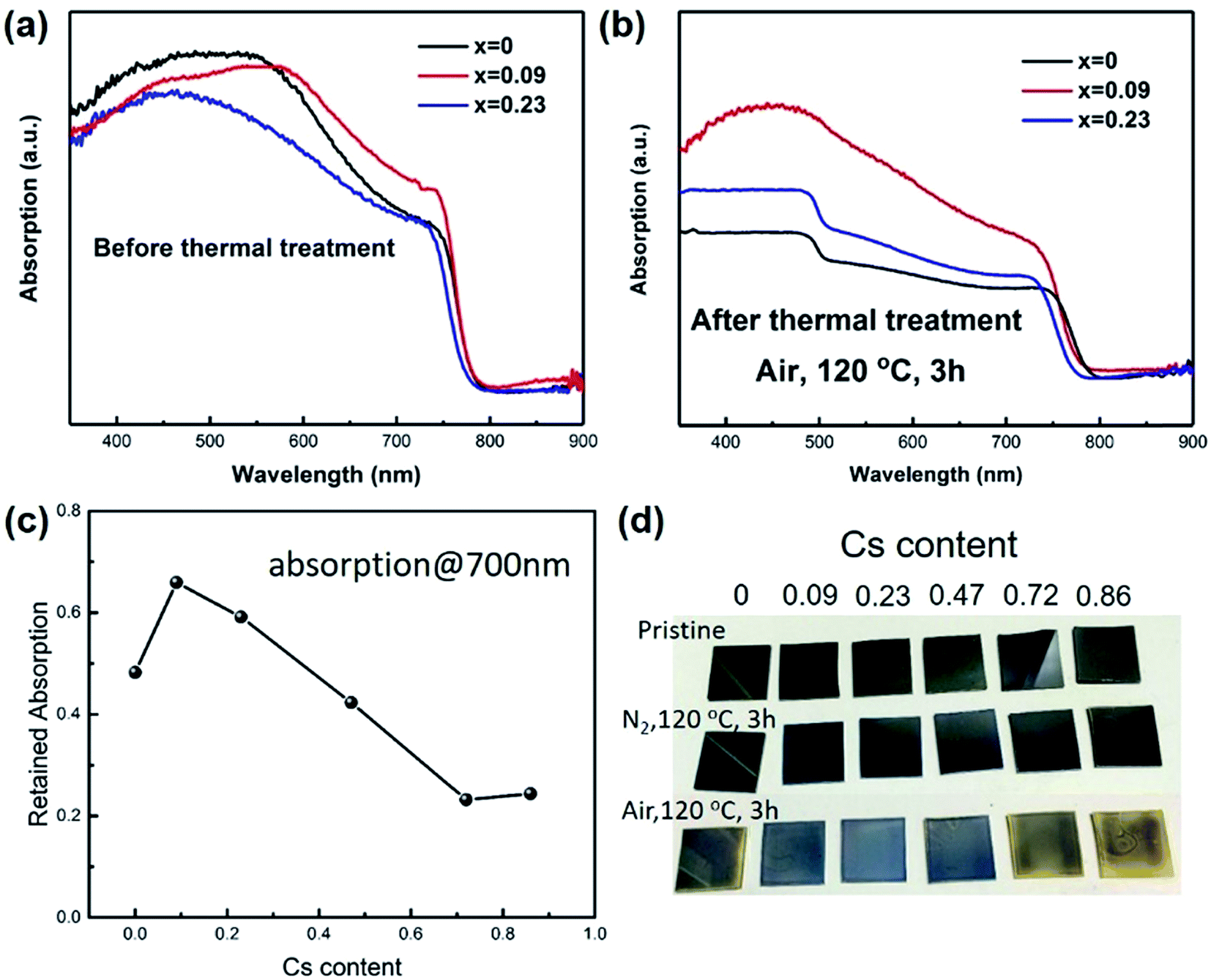 | ||
| Fig. 1 Thermal stability study of perovskite films with different Cs content. (a) Perovskite films with compositions of CsxMA1−xPbI3 before thermal treatment, where x represents Cs content. (b) Perovskite films after thermal treatment at 120 °C for 3 hours exposing to air. (c) Retained absorption at 700 nm for perovskite films with x ranging from 0 to 0.86. (d) Photographs of perovskite films exposing to different atmosphere. | ||
XRD patterns and SEM images were used to study the composition and morphology change of the film before and after thermal degradation. As shown in Fig. 2a, all the films demonstrated strongest intensity along 〈110〉/〈002〉 directions. Consistent with our previous results, as Cs doping increased, the peak for (112)/(200) planes became more obvious, which was due to that Cs atoms would preferentially precipitate and result in preferred crystal orientation along the more thermodynamically stable directions of 〈112〉/〈200〉.23 After thermal treatment (Fig. 2b), there was an additional new peak at 12.6°, which attributed to PbI2. For the control sample (x = 0), the peak for PbI2 was much higher than perovskite, demonstrating most of MAPbI3 has degraded to PbI2. For x = 0.09, the formation of PbI2 was effectively suppressed, due to the better thermal stability. For x = 0.23, in contrast, the peak for perovskite was even lower than that of x = 0.
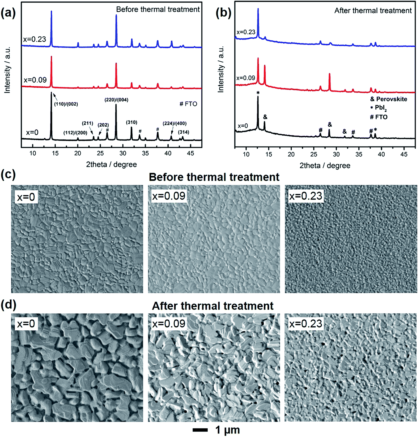 | ||
| Fig. 2 Structure analysis of perovskite films. (a, b) XRD patterns for CsxMA1−xPbI3 before and after thermal treatment. (c, d) Top-down view SEM images of perovskite films before and after thermal treatment. | ||
Fig. 2c and d shows the morphology of the films. Before thermal treatment, all the films were flat with no pinholes, while Cs content could lead to smaller grain size, probably due to the increased nucleation sites in the early stage of film formation. In contrast, after thermal treatment, the films became rugged, especially for x = 0. The pits and pinholes were caused by the loss of MAI or CH3NH2, leaving the film recrystallized as PbI2. When Cs was introduced into the film, the pinholes was effectively suppressed. In addition, as Cs content increased, the pinholes became smaller due to the much more stable A site (Cs) in the films and decreased crystal volume.
We assembled perovskite solar cells with x = 0 and x = 0.09, since if x > 0.09, the thermal stability was not good enough. As shown in Fig. 3a and b, the cross-sectional SEM images exhibited that the thickness of perovskite (x = 0.09) was ∼500 nm, including the mesoporous TiO2 layer and top perovskite layer, higher than that of x = 0 (405 nm). During the experiment, all the parameters were kept the same except the composition of precursor solution. The higher thickness of x = 0.09 was probably due to the increased film formation rate when Cs was introduced into the film. If the film formation rate was fast, more perovskite would precipitate out when chlorobenzene was added onto the film to quench the precursor solution. Due to the increased film thickness, the short-circuit current (JSC) of x = 0.09 was higher than that for x = 0. As shown in Table 2 and Fig. 3c, the champion device of x = 0.09 showed a JSC of 22.57 mA cm−2, a VOC of 1.06 V, FF of 0.76, leading to a final power conversion efficiency of 18.1%. In contrast, the champion device of control sample exhibited a JSC of 20.59 mA cm−2, a VOC of 1.04 V, FF of 0.74, and a PCE of 15.8%. Fig. 3d shows the IPCE spectra of the champion devices. Although Cs atoms could inevitably increase the band gap of perovskite, the absorption region was almost the same for x = 0 and 0.09 due to the small doping ratio. The integrated photocurrent for x = 0 and 0.09 was 18.6 and 19.9 mA cm−2, respectively, slightly lower than the value derived from J–V curves. The reason is that our devices exhibited hysteresis effect, while IPCE recorded the steady state current. We have also averaged data from 12 devices to obtain statistic information. The average JSC was increased from 20.34 ± 1.20 mA cm−2 for x = 0 to 22.42 ± 0.33 mA cm−2 for x = 0.09. Additionally, besides the increase of JSC after Cs introduction, the fill factors have also been increased from 0.70 ± 0.02 to 0.74 ± 0.01. During this work, we employed mesoporous TiO2 as anode and found hysteresis effect for the fabricated devices (Fig. S3†). Further improvement on suppressing hysteresis, such as using C60 or other fullerene derivatives, is undergoing. In order to illustrate the change of FF, we measured electrochemical impedance spectra (EIS) to study the internal electron recombination process. The response under light illuminations was analyzed at different applied voltages. Two semicircles and a low frequency feature are existing in the spectra (Fig. S2†). The first arc at higher frequencies attributes to the charge transfer in hole transport materials (HTM). The second one at lower frequencies is caused by the electron recombination at the interface of TiO2/perovskite/HTM. The low frequency feature is due to slow charge transport, which is not related to the device physics, and is not included in the analysis in this paper. The impedance spectra was fitted with a simplified equivalent circuit from the typical transmission line model for dye sensitized solar cells, as shown in the inset of Fig. S2.†23 The Rrec from the second arc represents the charge recombination barrier at the interface of TiO2/perovskite/HTM (Fig. 3e). It is acknowledged that the decreased trap states in the perovskite film could lead to reduced charge recombination. In this work, the charge recombination was suppressed when Cs was introduced into the film, which would be further verified through photoluminescence (PL) decay and X-ray photoelectron spectra (XPS). In addition, the charge lifetime could be obtained by Rrec × Crec from the second arc. It is found that the lifetime was also increased after Cs introduction (Fig. 3f). It could also be seen that as the Vappl increased, the recombination resistance and lifetime lowered, because of the upshift of the Fermi level of TiO2 and promoted electron transfer to perovskite and HTM.
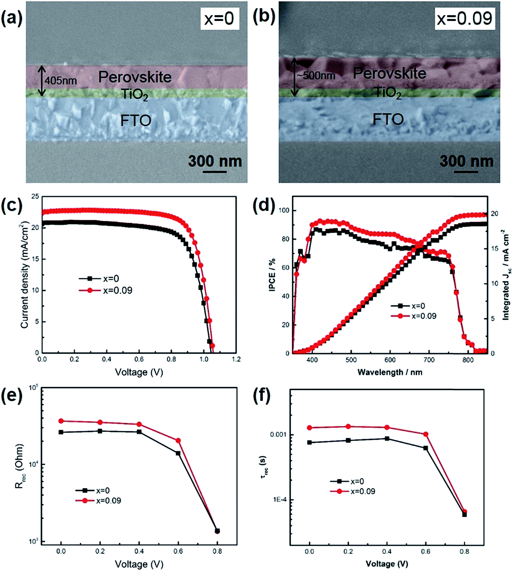 | ||
| Fig. 3 (a, b) Cross-sectional SEM images of perovskite films with x = 0 and 0.09. (c) J–V characteristics of champion devices with different Cs content. (d) IPCE and integrated photocurrent for the champion devices. (e) Recombination resistance derived from electrochemical impedance spectra (EIS). (f) Electron recombination time from EIS spectra. | ||
| JSC (mA cm−2) | VOC (V) | FF | η (%) | |
|---|---|---|---|---|
| x = 0 | 20.34 ± 1.2 | 1.05 ± 0.01 | 0.70 ± 0.02 | 14.9 ± 1.3 |
| Champion | 20.59 | 1.04 | 0.74 | 15.8 |
| x = 0.09 | 22.42 ± 0.33 | 1.05 ± 0.01 | 0.74 ± 0.01 | 17.5 ± 0.5 |
| Champion | 22.57 | 1.06 | 0.76 | 18.1 |
In order to explain the charge recombination effect by Cs introduction, we measured XPS spectra for the films (Fig. 4a). There are two main peaks for Pb 4f spectra, assigning to Pb 4f7/2 and Pb 4f5/2. For x = 0 sample, the peaks at 138.4 eV and 143.2 eV are due to Pb element from perovskite. The presence of small peaks at 136.9 eV and 141.3 eV could be assigned to metallic Pb (Pb0), which was due to unsaturated Pb, according to recent studies. Henry Snaith and co-workers demonstrated that the presence of unsaturated Pb atoms was related to the iodide deficiencies, and metallic lead species could act as recombination sites, leading to poor performance.26 In our assumption, during thermal annealing process, the loss of iodide was accompanied with the loss of methyl ammonium. When we replaced some MA with Cs atoms, due to the better thermal stability and thus less loss of molecular groups from A site and iodide atoms, unsaturated Pb was effectively suppressed. For XPS spectra of x = 0.09, there are no additional peaks from Pb0. Furthermore, we also measured transient photoluminescence spectra to study the defect density in the film (Fig. 4b). The decay curves could be well fitted by a biexponential decay function. The fast component is attributed to the surface recombination, while the slow component is caused by the recombination in the bulk of perovskite. We average the two components according to their amplitude to obtain the lifetime of carriers. The average corresponding decay time was 1.9 and 2.9 ns for x = 0, and 0.09 respectively, as shown in the inset of Fig. 4b. The increased lifetime when Cs was introduced into the film reflected the reduction of trap density, which was indicative of fewer non-radiative recombination sites.
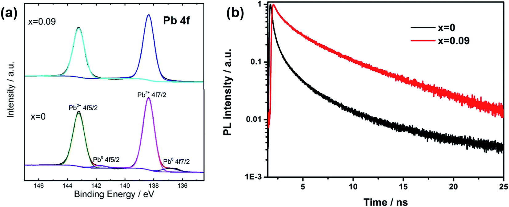 | ||
| Fig. 4 (a) XPS study of Pb4f for x = 0 and 0.09 films. (b) Transient PL spectra for perovskite films with different Cs content. | ||
At last, we compared the thermal stability of assembled perovskite solar cells for x = 0 and 0.09, as shown in Fig. 5. The accelerated stability of the devices is evaluated in air at 85 °C without encapsulation. Each time before measurement for J–V curves, the devices were cooled down to room temperature naturally. For x = 0, less than 40% of the original performance was maintained after 60 min aging test. In contrast, for x = 0.09, nearly 80% of the initial performance was retained after the same durability test. The data were averaged from 6 devices in one batch. There are two causes for the performance declination, one is coming from the degradation of perovskite, and the other one is from the degradation of spiro-MeOTAD under heat treatment. The glass transition temperature of spiro-MeOTAD is around 125 °C.11 We believe mixture of Cs and MA indeed improved the thermal stability. However, the existence of spiro-MeOTAD would inevitably lower the overall stability. Better stability toward thermal conditions could be obtained by replacing spiro-MeOTAD with other stable hole transport materials.
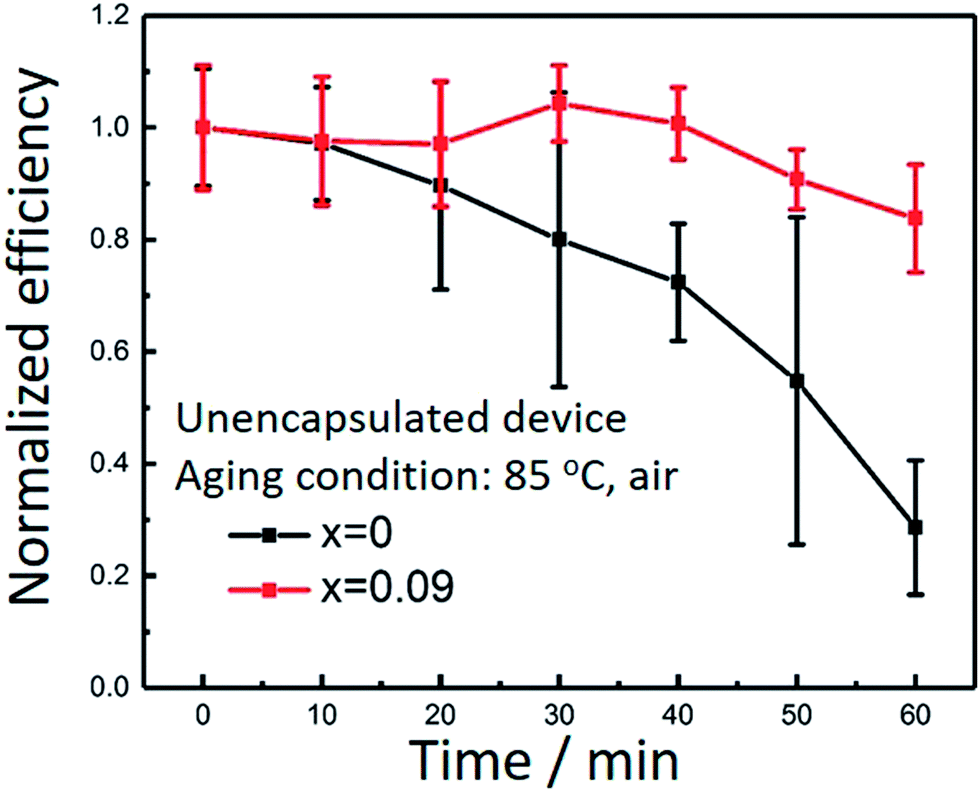 | ||
| Fig. 5 Thermal stability of assembled perovskite solar cells from Cs doping and undoped perovskite. | ||
Conclusions
In a word, we have successfully fabricated perovskite films with composition of CsxMA1−xPbI3. The introduction of Cs into the precursor solution would inevitably accelerate the film deposition rate. The results were that the grain size became smaller and the film contained more Cs atoms than in the precursors. The study on thermal stability illustrated that perovskite degradation was highly related with oxygen in air. Small amount of Cs doping (x = 0.09) was beneficial for the better thermal stability. In addition, Cs doping also enhanced the device performance. The improvement of short-circuit currents came from the increased film thickness, which was due to the faster deposition rate for Cs doped sample. Besides, Cs doping was vital to suppress the trap states in the film since the trap states was related to the halide deficiency during thermal annealing. At last, the final performance of Cs0.09MA0.91PbI3 reached 18.1%, with a JSC of 22.57 mA cm−2, VOC of 1.06 V, FF of 0.76. In addition, the thermal stability of the unencapsulated devices for x = 0.09 was also significantly improved compared to MAPbI3.Experimental details
Solar cell fabrications
The TiO2 compact layer was deposited onto FTO glass through atomic layer deposition (Beneq TFS 200) documented in previous reports. The mp-TiO2 layer was prepared by depositing nanocrystalline TiO2 paste (18NRT from Dyesol Company; diluted to w/w 14.3%) onto the compact layer at 6000 rpm for 30 s, followed by heating at 500 °C for 1 h. The perovskite precursors were prepared by dissolving specific amounts of PbI2, MAI, and CsI in the mixed solvent (γ-butyrolactone:DMSO = 7:3 vol%). The total concentration of Pb was set as 0.96 M for all the solutions. The solutions were then coated onto the substrate by two consecutive spin-coating steps, at 1500 rpm for 10 s, and 5000 rpm for 30 s. During the second step, 0.3 mL chlorobenzene was poured onto the substrate. Then the film was heated at 90 °C for 10 min. Spiro-MeOTAD solution was prepared by dissolving 102.7 mg spiro-MeOTAD in 1 mL chlorobenzene, to which 9.85 μL 4-tert-butyl pyridine and 42.22 μL lithium bis(trifluoromethanesulfonyl)imide solution (170 mg LITFSI in 1 mL acetonitrile) were added. Spiro-MeOTAD was deposited on the substrate at 2000 rpm for 45 s. Then the films were left in air overnight. Finally, 50 nm gold electrode were thermally evaporated under vacuum of ∼10−6 Torr, at a rate of ∼0.2 Å s−1.
Characterization
X-ray diffraction (XRD) spectra was measured with smart LAB instruments Cu Kα beam (λ = 1.54 Å). UV-Vis absorption spectra were obtained with a Hitachi U-3010 spectroscope. SEM images were measured by JEOL JSM-7401F and TEM images by Hitachi HT7700 with an acceleration voltage of 100 kV. The composition of the film was measured by ICP-AES (Thermo IRIS intrepid II). J–V curves were measured by a Keithley 2400 source meter under one sun illumination (AM 1.5G, 100 mW cm−2), simulated by a solar simulator (ORIEL 81193) calibrated with an NREL-calibrated silicon solar cell. External quantum efficiency (EQE) spectra were recorded by a setup, consist of a xenon light source, a monochromator, and a potentiostat. EIS were measured by an electrochemical workstation (Zahner, CIMPS) with frequency from 10 to 106 Hz under applied voltage with an amplitude of 10 mV under light condition. The active area of each cell was 0.16 cm2 with a mask of 0.09 cm2. Time-resolved PL decay was measured by a FV1200, excited at 488 nm.Acknowledgements
The research was funded by the National Natural Science Foundation of China under Grant no. 51273104 and 91433205.References
- A. Kojima, K. Teshima, Y. Shirai and T. Miyasaka, J. Am. Chem. Soc., 2009, 131, 6050 CrossRef CAS PubMed
.
- M. M. Lee, J. Teuscher, T. Miyasaka, T. N. Murakami and H. J. Snaith, Science, 2012, 338, 643 CrossRef CAS PubMed
- http://www.nrel.gov/ncpv/images/efficiency_chart.jpg
- H. S. Kim, C. R. Lee, J. H. Im, K. B. Lee, T. Moehl, A. Marchioro, S. J. Moon, R. Humphry-Baker, J. H. Yum, J. E. Moser, M. Grätzel and N. G. Park, Sci. Rep., 2012, 2, 591 Search PubMed
- J. Burschka, N. Pellet, S.-J. Moon, R. Humphry-Baker, P. Gao, M. K. Nazeeruddin and M. Grätzel, Nature, 2013, 499, 316 CrossRef CAS PubMed
- H. Zhou, Q. Chen, G. Li, S. Luo, T.-b. Song, H.-S. Duan, Z. Hong, J. You, Y. Liu and Y. Yang, Science, 2014, 345, 542 CrossRef CAS PubMed
- W. S. Yang, J. H. Noh, N. J. Jeon, Y. C. Kim, S. Ryu, J. Seo and S. I. Seok, Science, 2015, 348, 1234 CrossRef CAS PubMed
- H.-S. Kim, S. H. Im and N.-G. Park, J. Phys. Chem. C, 2014, 118, 5615 CAS
- J. H. Noh, S. H. Im, J. H. Heo, T. N. Mandal and S. I. Seok, Nano Lett., 2013, 13, 1764 CrossRef CAS PubMed
- G. Niu, W. Li, F. Meng, L. Wang, H. Dong and Y. Qiu, J. Mater. Chem. A, 2014, 2, 705 CAS
- G. Niu, X. Guo and L. Wang, J. Mater. Chem. A, 2015, 3, 8970 CAS
- M. Grätzel, Nat. Mater., 2014, 13, 838 CrossRef PubMed
- X. Li, M. Tschumi, H. Han, S. S. Babkair, R. A. Alzubaydi, A. A. Ansari, S. S. Habib, M. K. Nazeeruddin, S. M. Zakeeruddin and M. Grätzel, Energy Technol., 2015, 3, 551 CrossRef CAS
- F. Bella, G. Griffini, J.-P. Correa-Baena, G. Saracco, M. Grätzel, A. Hagfeldt, S. Turri and C. Gerbaldi, Science DOI:10.1126/science.aah4046
- J. You, L. Meng, T.-B. Song, T.-F. Guo, Y. Yang, W.-H. Chang, Z. Hong, H. Chen, H. Zhou, Q. Chen, Y. Liu, N. D. Marco and Y. Yang, Nat. Nanotechnol., 2016, 11, 75 CrossRef CAS PubMed
- W. Chen, Y. Wu, Y. Yue, J. Liu, W. Zhang, X. Yang, H. Chen, E. Bi, I. Ashraful, M. Grätzel and L. Han, Science, 2015, 350, 944 CrossRef CAS PubMed
- Y. Shao, Y. Yuan and J. Huang, Nat. Energy, 2016, 1, 15001 CrossRef CAS
- J. W. Lee, D. H. Kim, H. S. Kim, S. W. Seo, S. M. Cho and N. G. Park, Adv. Energy Mater., 2015, 5, 1501310 CrossRef
- G. E. Eperon, S. D. Stranks, C. Menelaou, M. B. Johnston, L. M. Herz and H. J. Snaith, Energy Environ. Sci., 2014, 7, 982 CAS
- G. E. Eperon, G. M. Paternò, R. J. Sutton, A. Zampetti, A. A. Haghighirad, F. Cacialli and H. J. Snaith, J. Mater. Chem. A, 2015, 3, 19688 CAS
- R. E. Beal, D. J. Slotcavage, T. Leijtens, A. R. Bowring, R. A. Belisle, W. H. Nguyen, G. F. Burkhard, E. T. Hoke and M. D. McGehee, J. Phys. Chem. Lett., 2016, 7, 746 CrossRef CAS PubMed
- Q. Ma, S. Huang, X. Wen, M. A. Green and A. W. Y. Ho-Baillie, Adv. Energy Mater., 2016, 6, 1502202 CrossRef
- G. Niu, H. Yu, J. Li, D. Wang and L. Wang, Nano Energy, 2016, 27, 87 CrossRef CAS
- M. Saliba, M. Tsisuke, J.-Y. Seo, K. Domanski, J.-P. Correa-Baena, M. K. Nazeeruddin, S. M. Zakeeruddin, W. Tress, A. Abate, A. Hagfeldt and M. Grätzel, Energy Environ. Sci., 2016, 9, 1989 CAS
- C. Yi, J. Luo, S. Meloni, A. Boziki, N. Ashari-Astani, C. Gratzel, S. M. Zakeeruddin, U. Röthlisberger and M. Grätzel, Energy Environ. Sci., 2016, 9, 656 CAS
- W. Zhang, S. Pathak, N. Sakai, T. Stergiopoulos, P. K. Nayak, N. K. Noel, A. A. Haghighirad, V. M. Burlakov, D. W. deQuilettes, A. Sadhanala, W. Li, L. Wang, D. S. Ginger, R. H. Friend and H. J. Snaith, Nat. Commun., 2015, 6, 10030 CrossRef CAS PubMed
- N. Pellet, P. Gao, G. Gregori, T.-Y. Yang, M. K. Nazeeruddin, J. Maier and M. Grätzel, Angew. Chem., Int. Ed., 2014, 53, 3151 CrossRef CAS PubMed
- E. J. Juarez-Perez, Z. Hawash, S. R. Raga, L. K. Ono and Y. Qi, Energy Environ. Sci., 2016, 9, 3406 CAS
- B. Conings, J. Drijkoningen, N. Gauquelin, A. Babayigit, J. D'Haen, L. D'Olieslaeger, A. Ethirajan, J. Berbeeck, J. Manca, E. Mosconi, F. D. Angelis and H.-G. Boyen, Adv. Energy Mater., 2015, 5, 1500477 CrossRef
Footnote |
| † Electronic supplementary information (ESI) available. See DOI: 10.1039/c6ra28501e |
| This journal is © The Royal Society of Chemistry 2017 |