DOI:
10.1039/C4RA14321C
(Paper)
RSC Adv., 2015,
5, 3786-3791
Perovskite solar cell with low cost Cu-phthalocyanine as hole transporting material
Received
11th November 2014
, Accepted 5th December 2014
First published on 5th December 2014
Abstract
Low cost copper phthalocyanine has been used as hole-transporting material for the construction of organolead halide solid state perovskite solar cells. The cells were assembled and tested under ambient conditions. They achieved a power conversion efficiency of 5.0% using copper phthalocyanine, which appears to have potential to replace the currently used organic hole transporters. The present work has also examined the possibility of upscaling by construction of small cell modules.
Introduction
The fast growth of the planet's population has caused an increase in energy consumption and an ever increasing demand. It has been estimated that by 2050 the energy gap will be around 15 TW.1 The increased consumption of fossil fuels to meet energy demands is considered as the main reason for the greenhouse effect and global warming. Under these conditions, solar energy in all its useable forms gains more and more importance. Solar energy is clean, reliable and renewable and it can respond to future demands since the amount of solar energy that strikes the surface of the earth in one hour is enough to cover the energy consumption worldwide in one year.2 One direct way to exploit solar energy is to convert it into electricity by using solar cells. A wide range of solar cell technologies are being investigated and developed in the recent years, which includes dye-sensitized solar cells,3 bulk heterojunction solar cells,4 depleted heterojunction solar cells,5,6 hybrid organic–inorganic solid state solar cells,7–10 etc. In the present work, we deal with the last category, where light harvesting is mainly achieved with the help of a quantum dot semiconductor sensitizer. In this type of cells, the sensitizer is placed between the electron conducting material, which in the present and in most cases is a n-type nanostructured metal oxide semiconductor,11 and the hole transporting phase, which is usually made of an organic material. The sensitizer injects negative and positive charge carriers in the respective electronic transport materials while the photocurrent is collected at the front and back contacts of the solar device. The obtained photo-voltage is the result of the difference between the quasi-Fermi levels of the electron and hole-conducting phases under illumination.
Organometal halide perovskites have attracted a strong scientific interest as components of solar cells due to their excellent optical and conductivity properties. Their chemical structure can be represented by AMX3, where A is usually an organic ammonium cation, M a metal and X is a halide anion.12 By making unprecedentedly fast steps, researchers of organometal halide perovskite solar cells have managed to reach solar cell efficiencies that overpassed traditional photovoltaic solar cells. Thus in 2009, Kojima et al.13 published a 3.8% power conversion efficiency using perovskites as the sensitizing material for DSSCs, while Im et al.14 obtained 6.5% efficiency with the same type of materials. In 2012, an inorganic perovskite, CsSnI3, was used by Chung et al.15 as a hole conductor for solid state DSSCs. By employing CH3NH3Pbl2Br perovskite and spiro-OMeTAD as the hole transporting material Kim et al.16 reached an efficiency of 9.7% while Heo et al.8 reported 12% efficiency using CH3NH3PbI3, TiO2 and a polymeric hole conductor. Snaith and co-workers reduced the processing temperature of the bulk absorber layer in CH3NH3PbI3−xClx perovskite solar cells and achieved power conversion efficiencies of up to 12.3%.17 Gratzel and coworkers recently reported 15% efficiency with CH3NH3PbI3 perovskites and spiro-OMeTAD using a two-step deposition method18 while Snaith and coworkers with vacuum deposited CH3NH3PbClxI3−x reported efficiency of 15.4%.19 Gratzel, Park and coworkers reported champion efficiency of 17.01% with two step spin coating procedure by size-controlled growth of CH3NH3PbI3 cuboids.20 Finally, a world record efficiency of 19.3% has been achieved by Y. Yang and co-workers for the system ITO-polyethyleneimine/Y:TiO2/CH3NH3PbI3−xClx/spiro-OMeTAD/Au.21
Concerning hole transporting materials, molecular Spiro-OMETAD,22 polymeric transporters8,23 and inorganic materials24,25 have been used to make solid state solar cells including perovskite solar cells. Most of the hole transporting materials do not show absorption in the Visible and NIR region. Some of the polymers, like polythiophene, do absorb visible light and may participate in the sensitization process, even though, in the presence of organometal halide perovskites this type of sensitization is of minor importance. The main problem with these materials is their high cost, which dictates a need for the search of alternative hole conductors. Inorganic hole conductors may offer inexpensive alternatives and they have been recently studied with satisfactory results.24,25 In the present work, a low cost and easy to manipulate molecular hole conductor, copper phthalocyanine (CuPc) has been studied as a component of organometal halide perovskite solar cells. CuPc is, thermally and chemically, very stable. CuPc has already been used as a p-type semiconductor and attracted attention because of its flexibility, color, stability, semiconducting property and cost-effective applications.26–28
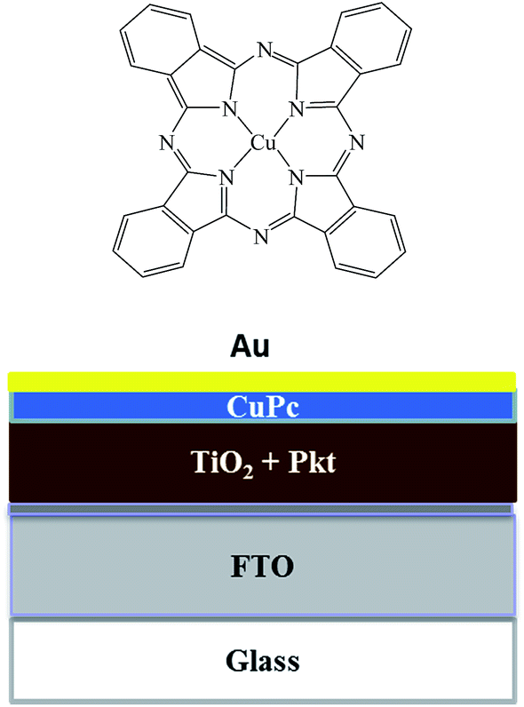
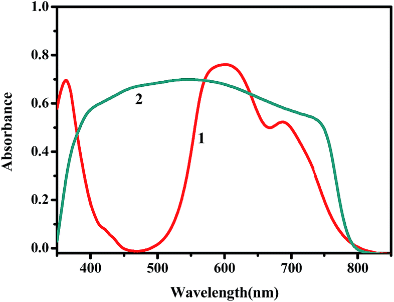
The molecular structure of copper phthalocyanine is shown in Fig. 1. Its visible absorption lies between 500 to 800 nm (Fig. 2) and for this reason it has a blue color. CuPc possesses a large π-conjugated system that makes it difficult to dissolve in most commonly used organic solvents. Thus it is rarely studied by traditional spin coating techniques. CuPc has been used as material in vacuum deposited OPV devices due to high absorption coefficient and long exciton diffusion length.29–32 The CuPc/C60 combination is among the most common small molecule organic solar cells and has exhibited satisfactory performance.33
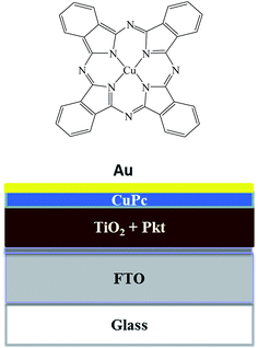 |
| | Fig. 1 Molecular structure of Cu phthalocyanine and device layer structure of the perovskite solar cell. | |
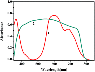 |
| | Fig. 2 UV-vis absorption spectra of (1) CuPc thin film and (2) TiO2/CH3NH3PbClxI3−x film (after subtracting absorption due to titania alone). | |
In the present work CuPc has been deposited by vacuum deposition. It has been used as hole-transporting material to make small laboratory size solar cells but also to construct small perovskite solar cell modules. One serious drawback of organometal halide perovskites is their vulnerability to humidity that necessitates synthesis under dry conditions and encapsulation for further protection from humidity. For sure, this fact will increase cost when perovskite solar cells make it to the market. In addition, the reported efficiencies refer to tiny cells of only a few square millimeters of active surface. It is well known that the efficiency drops when the size of the cell increases. It is then necessary not only to race for higher efficiencies but also to appreciate the difficulties of upscaling. For this reason in the present work, we have studied perovskite solar cells, which were partly made under ambient conditions and under a limited upscaling. We believe that this effort will set lower limit conditions and define realistic terms for the construction of perovskite solar cells.
Results and discussion
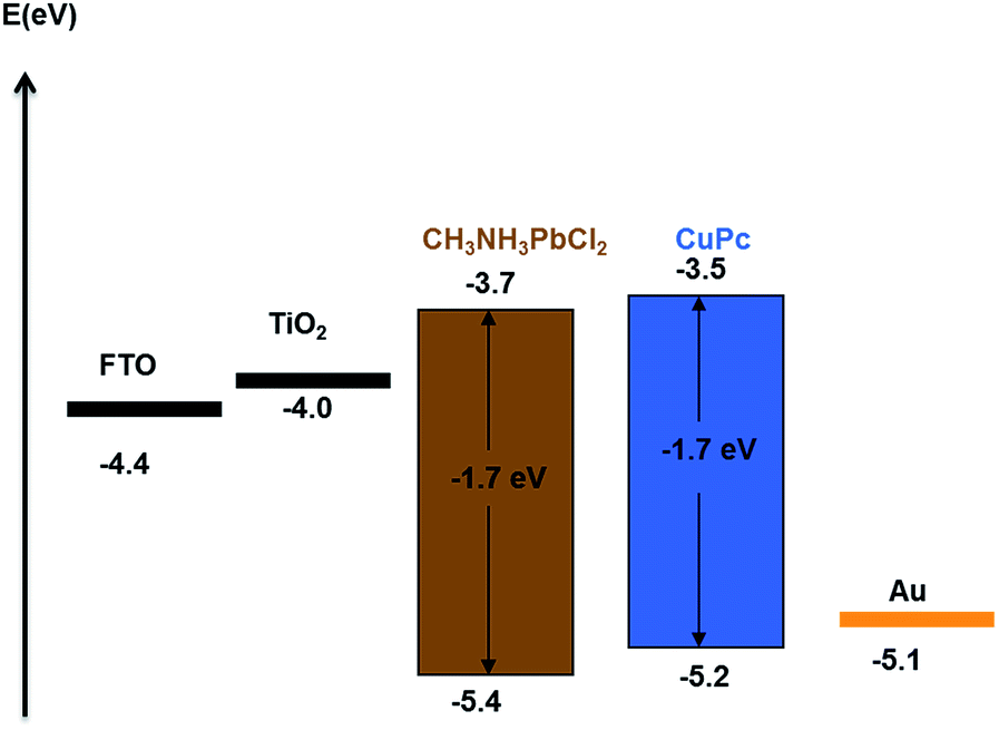
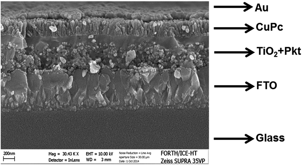
Fig. 2 shows the UV-vis absorption spectra of CH3NH3PbClxI3−x and CuPc films. It is seen that the strong absorbance of the perovskite covers the whole of the visible spectrum and it may mask any light absorption by the CuPc film.34 The device architecture is schematically presented in Fig. 1, while details are given in the Experimental section. Mesoporous titania plays the role of scaffold for supporting the perovskite and simultaneously the role of collector of the photogenerated in the perovskite electrons. In turn CuPc, placed on the top of the TiO2/CH3NH3PbClxI3−x, plays the role of photogenerated hole collector. These roles are justified by the energy diagram of Fig. 3. In fact the placement of the energy states is ideal for electron injection into the titania conduction band and hole injection into the CuPc LUMO. This matching of energy levels is a prerequisite of cell functioning and, as it will be shown below, it was very successful in the present case. Successful combination of materials additionally necessitates a good contact between the subsequent layers and good formation of the layered structure without defects. In this respect, Fig. 4 also reveals a very smooth deposition and uniformity of structure that is expected to favor cell performance.
 |
| | Fig. 3 Energy level diagram of perovskite solar cells with CuPc hole conductor.35,36 | |
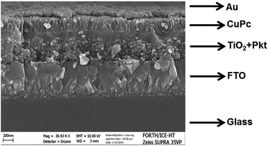 |
| | Fig. 4 FESEM image of a cross section of the TiO2/CH3NH3PbClxI3−x/CuPc/Au solar cell. The scale bar is 200 nm. Pkt stands for perovskite. | |
The composition of the CH3NH3PbClxI3−x perovskite deposited under the present conditions was examined by using EDX spectra. A characteristic example is presented by Fig. 5. Based on these data, the closest approximate structure of the presently obtained perovskite sensitizer can be represented by the following formula: CH3NH3PbClI2. This means that the spontaneous uptake of chlorine under the present conditions is smaller than the one present in the precursor solution (see Experimental section). Indeed, the atomic ratio of Pb![[thin space (1/6-em)]](https://www.rsc.org/images/entities/char_2009.gif) :Cl:I in the precursor solution was 1:2:3 but the corresponding ratio detected by EDX was 1:1.1:2.2. Obviously, the majority of the presently formed perovskites involve one chlorine and two iodine atoms.
:Cl:I in the precursor solution was 1:2:3 but the corresponding ratio detected by EDX was 1:1.1:2.2. Obviously, the majority of the presently formed perovskites involve one chlorine and two iodine atoms.
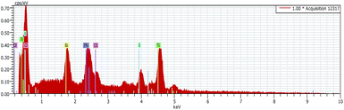 |
| | Fig. 5 Energy-dispersive X-ray spectroscopy analysis (EDX) of a sensitized photoanode. Atomic percent: (O)50.7; (Ti)25.1; (Pb)3.6; (Cl)4.1; and (I)7.9. | |
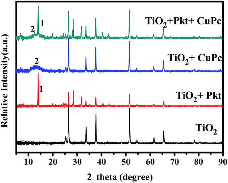
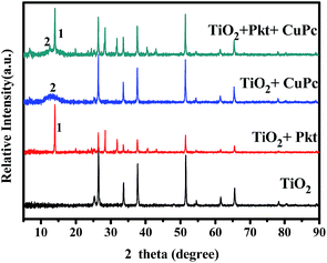
The active components of the cell have been also characterized by XRD at various materials combinations, as seen in Fig. 6. The lower XRD spectrum gives the usual peaks expected for pure titania films,37 however, the prevailing lines belong to the FTO substrate. This is because the presently used titania film is very thin and gives small contribution. When the perovskite was added, clearly new and well defined peaks showed up, indicating that CH3NH3PbClxI3−x obtains a crystalline structure.38 On the contrary, addition of CuPc did not produce any new peaks. For this reason, CuPc was also deposited alone on a titania film also by vacuum evaporation and again did not produce any new lines. We then concluded that this material is amorphous. A very broad peak appearing around 14° may indicate some limited small nanoparticle formation but apparently this is not the rule.
 |
| | Fig. 6 X-ray diffraction spectra of the active cell components deposited in various combinations. | |
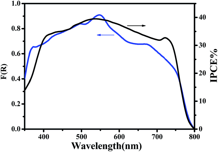
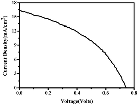
The current–voltage (J–V) characteristics of the small unit solar cells measured under simulated solar radiation are shown in Fig. 7, while the corresponding photovoltaic parameters are summarized in Table 1. The best performing cell demonstrated a short circuit current density (Jsc) of 16.3 mA cm−2, an open circuit voltage (Voc) of 0.75 V and a fill factor of 40% leading to a PCE of 5%. Table 1 also shows average values obtained over several cells made under the same conditions. In general, cells gave a satisfactory open-circuit voltage, justified by the relatively large difference between the two charge acceptor levels, i.e. the conduction band of titania and the LUMO level of CuPc.35 This difference is 1.2 Volts (Fig. 3) indicating that there is still room for improvement. The current density was relatively large, as it is usually obtained with CH3NH3PbClxI3−x perovskites, which absorb light in the whole visible range and into the near IR. Indeed, as seen by the IPCE spectrum and the cell absorption spectrum shown in Fig. 8, the cell is active over the whole visible and NIR and this justifies high currents. A small but well distinguished peak of the IPCE spectrum in the NIR indicates some contribution to sensitization by CuPc, in addition to its main role as hole transporter. However, the major sensitizer is perovskite (cf. Fig. 2). The fill factor of the cell was relatively small and this is the main reason for the rather limited cell efficiency, compared to the efficiencies obtained with perovskite solar cells made with spiro-OMeTAD as hole transporter. Apparently the cell has a low shunt resistance39 and this must be eventually improved. Of course, the present data were recorded under ambient conditions without encapsulation while perovskite was synthesized also under ambient conditions of mild humidity. This adds to limitations in cell performance but it also offers a way to set lower limits for cell fabrication conditions.
 |
| | Fig. 7 Current–voltage characteristics of the solar cells with Cu phthalocyanine as the hole transporting material measured under ∼100 mW cm−2 simulated solar radiation. | |
Table 1 Photovoltaic characteristics of small unit cells
| Cell |
Voc (V) |
Jsc (mA cm−2) |
FF (%) |
η (%) |
| Most efficient cell |
0.75 |
16.3 |
40 |
5.0 |
| Maximum current cell |
0.57 |
19.9 |
39 |
4.4 |
| Average over several cells |
0.71 |
14.7 |
35 |
3.7 |
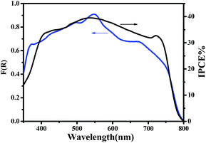 |
| | Fig. 8 Absorption spectra and IPCE values of perovskite solar cells. The absorption spectrum was recorded with a film containing all active components except the top Au electrode while the IPCE spectrum corresponds to a complete cell. | |
Unit cells were combined to form cell modules, as seen in Fig. 9. Fig. 9 also shows the architecture of cell combinations. 6 unit cells were combined in parallel and two rows were combined in series. The photovoltaic characteristics of these cells are summarized in Table 2. The total current produced by each row of 6 cells was 8.9 mA. The actual current of each unit cell of Table 1 was 2.4 mA. Therefore, 8.9 mA are substantially smaller than the expected 6 × 2.4 = 14.4 mA. This loss of current is, however, expected and is observed when upscaling is attempted on small unit cells. The lower current is due to several reasons: overestimation of the current produced by a unit cell, which is usually larger than the area defined by the electrodes; small conductivity of the FTO electrodes; lateral diffusion of current and loss by trapping, etc. In the present case a loss of voltage and a drop of the fill factor were also observed by parallel connection, which is most probably due to fabrication deficiencies under the present conditions. On the other hand, connection of two rows in series did give a voltage multiplication and current preservation. Overall, the results are encouraging and it is obvious that interesting photovoltaic characteristics can be obtained by these small cell modules.
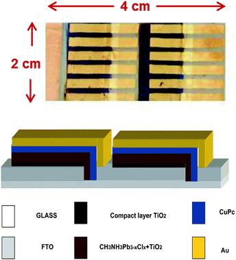 |
| | Fig. 9 Photograph of cell module comprising 6 unit cells connected in parallel with two rows in series and schematic representation of device architecture. | |
Table 2 Photovoltaic characteristics of cell modules
| Device description |
Voc (Volts) |
Isc (mA) |
FF (%) |
| 6 unit cells connected in parallel and two modules in series |
1.08 |
8.8 |
28 |
| 6 unit cells connected in parallel in first module |
0.61 |
8.9 |
28 |
Experimental
Materials
All materials were purchased from Aldrich, unless otherwise specified, and they were used as received. FTO glasses of 8 ohm/square were purchased from Pilkington.
Fabrication of perovskite solar cells
FTO-coated glass substrates were cut in the dimensions of 1 × 3 cm. One third of the conductive layer was removed using zinc power and hydrochloric acid. Then they were washed with detergent, rinsed several times with distilled water and subsequently with ethanol in an ultrasonic bath, finally dried under air stream. A compact thin layer of TiO2 was deposited by aerosol spray pyrolysis using a solution of 0.2 M diisopropoxytitanium bis(acetylacetonate) in EtOH. After spraying, the samples were heated for 1 hour at 500 °C. Subsequently, a mesoporous TiO2 layer composed of titania paste made of P25 nanoparticles was spin coated at 4000 rpm for 30 seconds and then heated for 15 minutes at 500 °C. A layer of TiCl4, was then deposited by dipping the electrode into a solution made of 0.04 M TiCl4 in H2O for 30 minutes, then copiously rinsing and finally calcining at 500 °C. Active perovskite layer was deposited on the thus prepared titania film by modifying published procedures.5 Methylammonium iodide was first synthesized by mixing 27.8 ml of methylamine (40 wt% in H2O) and 30 ml of hydroiodic acid (57 wt% in water) and let interact at 0 °C for 2 hours. The precipitate was recovered by evaporating the solution in a rotary evaporator at 40 °C. The yellow crude product methylammonium iodide (CH3NH3I) was washed with diethyl ether several times, and then finally recrystallized from a mixed solvent of diethyl ether and ethanol. After filtration, the pure solid was collected and dried at 70 °C in a vacuum oven overnight. A precursor solution was made by mixing 230 mg PbCl2 with 394 mg methyl ammonium iodide in 1 ml of DMF. The atomic ratio Pb:Cl:I in the precursor solution was thus 1:2:3. The solution was kept under stirring for about half an hour and then it was deposited by spin coating at 6000 rpm for 90 seconds under ambient conditions of 50–60% relative humidity. Heating at 80 °C for about half an hour made the sample's color turn from yellow to black. Hole-transporting CuPc layer was deposited by vacuum thermal evaporation. The last step was the deposition of 80 nm thick gold electrodes also by thermal evaporation under vacuum. These unit devices had an active size of 15 mm2 (10 mm × 1.5 mm) as defined by the size of the gold electrodes. A schematic representation of cell components is shown in Fig. 1 while a FESEM cross-sectional image is shown in Fig. 4.
Fabrication of small cell module
A small cell module has been fabricated by combining 6 unit cells in parallel and 2 rows in series. A picture of the module is shown in Fig. 9. Electric contacts were made by using auto-adhesive copper ribbons. Fabrication of the module was carried out by employing the same deposition techniques as for the unit cells.
Characterization-methods
Illumination of the samples was made with a PECCELL PEC-L01 Solar Simulator set at 100 mW cm−2. J–V characteristic curves were recorded under ambient conditions with a Keithley 2601 source meter that was controlled by Keithley computer software (LabTracer). IPCE values were obtained with an Oriel IQE 200 system. UV-vis absorption spectra were recorded using a Shimadzu model 2600 spectrophotometer equipped with an integration sphere. FESEM/EDX images were obtained with a Zeiss SUPRA 35VP with a field emission gun equipped with an EDX system (QUANTA 200, Bruker AXS) and X-ray diffraction measurements were made using a X-ray diffractometer (D8 Advance) Bruker.
Conclusions
Solid state perovskite solar cells can be constructed by using relatively inexpensive reagents and simple inexpensive procedures by employing copper phthalocyanine as hole transporting material. Small unit cells can be upscaled under the same deposition procedures as for small unit cells. The cell performance suffers of very low fill factors that need to be improved by improving cell fabrication procedures.
Acknowledgements
The present work was supported by the project 11SYN_7_298, implemented under the Act “COOPERATION 2011 – Partnerships of Production and Research Institutions in Focused Research and Technology” of the Operational Programmes “Competitiveness and Entrepreneurship (EPAN II)” and “Regions in Transmission (NSFR 2007–13)”. The authors are very thankful to Dr V. Dracopoulos for his help with XRD and FESEM measurements.
Notes and references
- C. Gratzel and S. M. Zakeeruddin, Mater. Today, 2013, 16, 11–18 CrossRef CAS PubMed.
- O. Morton, Nature, 2006, 443, 19–22 CrossRef CAS PubMed.
- M. Gratzel, J. Photochem. Photobiol., A, 2004, 164, 3–14 CrossRef CAS PubMed.
- D. Liu and T. L. Kelly, Nat. Photonics, 2014, 8, 133–138 CrossRef CAS.
- L. Etgar, P. Gao, Z. S. Xue, Q. Peng, A. K. Chandiran, B. Liu, M. K. Nazeeruddin and M. Grätzel, J. Am. Chem. Soc., 2012, 134, 17396–17399 CrossRef CAS PubMed.
- W. A. L. Laban, Energy Environ. Sci., 2013, 6, 3249–3253 CAS.
- G. Sfyri, S. Sfaelou, K. S. Andrikopoulos, N. Balis, G. A. Voyiatzis and P. Lianos, J. Phys. Chem. C, 2014, 118, 16547–16551 CAS.
- J. H. Heo, S. H. Im, J. H. Noh, T. N. Mandal, C.-S. Lim, J. A. Chang, Y. H. Lee, H. Kim, A. Sarkar, M. K. Nazeeruddin, M. Grätzel and S. Seok II, Nat. Photonics, 2013, 7, 486–491 CrossRef CAS.
- M. M. Lee, J. Teuscher, T. Miyasaka, T. N. Murakami and H. J. Snaith, Science, 2012, 338, 643–647 CrossRef CAS PubMed.
- J. A. Christians, R. C. M. Fung and P. V. Kamat, J. Am. Chem. Soc., 2014, 136, 758–764 CrossRef CAS PubMed.
- H. S. Kim, C. R. Lee, J. H. Im, K. B. Lee, T. Moehl, A. Marchioro, S. J. Moon, R. Humphry Baker, J. H. Yum, J. E. Moser, M. Grätzel and N. G. Park, Sci. Rep., 2012, 2, 591–597 Search PubMed.
- L. C. Schmidt, A. Pertegás, S. González-Carrero, O. Malinkiewicz, S. Agouram, G. M. Espallargas, H. J. Bolink, R. E. Galian and J. Pérez-Prieto, J. Am. Chem. Soc., 2014, 136, 850–853 CrossRef CAS PubMed.
- A. Kojima, K. Teshima, Y. Shirai and T. Miyasaka, J. Am. Chem. Soc., 2009, 131, 6050–6051 CrossRef CAS PubMed.
- J. H. Im, C. R. Lee, J. W. Lee, S. W. Park and N. G. Park, Nanoscale, 2011, 3, 4088–4093 RSC.
- I. Chung, B. Lee, J. He, R. P. H. Chang and M. G. Kanatzidis, Nature, 2012, 485, 486–489 CrossRef CAS PubMed.
- H. S. Kim, S. H. Im and N. G. Park, J. Phys. Chem. C, 2014, 118, 5615–5625 CAS.
- J. M. Ball, M. M. Lee, A. Hey and H. J. Snaith, Energy Environ. Sci., 2013, 6, 1739–1743 CAS.
- J. Burschka, N. Pellet, S.-J. Moon, H. Baker, P. Gao, M. K. Nazeeruddin and M. Gratzel, Nature, 2013, 499, 316–319 CrossRef CAS PubMed.
- M. Liu, M. B. Johnston and H. J. Snaith, Nature, 2013, 501, 395–398 CrossRef CAS PubMed.
- J. H. Im, I. H. Jang, N. Pellet, M. Grätzel and N. G. Park, Nat. Nanotechnol., 2014, 9, 927–932 CrossRef PubMed.
- H. Zhou, Q. Chen, G. Li, S. Luo, T.-B. Song, H.-S. Duan, Z. Hong, J. You, Y. Liu and Y. Yang, Interfacial Sci., 2014, 345, 542–546 CAS.
- N. J. Jeon, J. Lee, J. H. Noh, M. K. Nazeeruddin, M. Grätzel and S. I. Seok, J. Am. Chem. Soc., 2013, 135, 19087 CrossRef CAS PubMed.
- J. H. Noh, S. H. Im, J. H. Heo, T. N. Mandal and S. I. Seok, Nano Lett., 2013, 13, 1764–1769 CAS.
- J. A. Christians, R. C. M. Fung and P. V. Kamat, J. Am. Chem. Soc., 2014, 136, 758–764 CrossRef CAS PubMed.
- P. Qin, S. Tanaka, S. Ito, N. Tetreault, K. Manabe, H. Nishino, M. K. Nazeeruddin and M. Gratzel, Nat. Commun., 2014, 5, 3834–3839 CAS.
- A. R. Murphy and J. M. J. Fréchet, Chem. Rev., 2007, 107(4), 1066–1096 CrossRef CAS PubMed.
- J. Zaumseil and H. Sirringhaus, Chem. Rev., 2007, 107, 1296–1323 CrossRef CAS PubMed.
- Y. Sun, Y. Liu and D. Zhu, J. Mater. Chem., 2005, 15, 53–65 RSC.
- T. Stubinger and W. Brutting, J. Appl. Phys., 2001, 90, 3632–3641 CrossRef CAS PubMed.
- P. Peumans and S. R. Forrest, Appl. Phys. Lett., 2001, 79, 126–128 CrossRef CAS PubMed.
- J. G. Xue, S. Uchida, B. P. Rand and S. R. Forrest, Appl. Phys. Lett., 2004, 84, 3013–3015 CrossRef CAS PubMed.
- J. Xue, S. Uchida, B. P. Rand and S. R. Forrest, Appl. Phys. Lett., 2004, 85, 5757–5759 CrossRef CAS PubMed.
- J. Xue, B. P. Rand, S. Uchida and S. R. Forrest, Adv. Mater., 2005, 17, 66–71 CrossRef CAS.
- C. F. Lin, M. Zhang, S. W. Liu, T. L. Chiu and J. H. Lee, Int. J. Mol. Sci., 2011, 12, 476–505 CrossRef CAS PubMed.
- K. Thamaphat, P. Limsuwan and B. Ngotawornchai, Nat. Sci., 2008, 42, 357–361 Search PubMed.
- S. Chavhan, O. Miguel, H. J. Grande, V. Gonzalez-Pedro, R. S. Sánchez, E. M. Barea, I. Mora-Seró and R. Tena-Zaera, J. Mater. Chem. A, 2014, 2, 12754–12760 CAS.
- H. Derouiche, S. Said and A. Mohamed, Smart Grid Renewable Energy, 2011, 2, 278–281 CrossRef CAS.
- P. Schulz, E. Edri, S. Kirmayer, G. Hodes, D. Cahen and A. Kahn, Energy Environ. Sci., 2014, 7, 1377–1381 CAS.
- Q. Jiang, X. Sheng, B. Shi, X. Feng and T. Xu, J. Phys. Chem. C, 2014, 118, 25878–25883 CAS.
|
| This journal is © The Royal Society of Chemistry 2015 |