
Organic–inorganic hybrid perovskite materials and their application in transistors
Yiran
Liu
 ab,
Yunqi
Liu
ab and
Yunlong
Guo
*ab
ab,
Yunqi
Liu
ab and
Yunlong
Guo
*ab
aBeijing National Laboratory for Molecular Sciences, Key Laboratory of Organic Solids, Institute of Chemistry Chinese Academy of Sciences, Beijing 100190, P. R. China. E-mail: guoyunlong@iccas.ac.cn
bSchool of Chemistry and Chemical Engineering, University of Chinese Academy of Sciences, Beijing 100049, P. R. China
First published on 19th July 2023
Abstract
The emerging hybrid organic–inorganic perovskites (HOIPs) have attracted significant attention owing to their versatile and tunable structures and properties. Employing organic cations, HOIPs can integrate the advantages of both organic and inorganic components. To date, HOIPs have been widely investigated in various fields, including photovoltaics, light-emitting devices, and field-effect transistor (FETs). HOIPs possess characteristics similar to conventional inorganic semiconductors, such as high charge carrier mobility and long diffusion length. Moreover, the capacity of solution processing ensures the facile fabrication of devices. Those advantages make HOIP materials a promising candidate for semiconductors in FETs. The first HOIP-based FET was reported in 1999, which was ten years earlier than the first HOIP-based solar cell. However, currently, reports on perovskite FETs are relatively rare, possibly due to the environment-dependent apparent mobilities, instability, and hysteresis caused by the intrinsic properties of perovskites. In this review, we aim to summarize the strategies developed by the pioneering works to improve the performances of HOIP-based FETs. We begin by providing a brief introduction to structure, properties, and versatile fabrication methods. Afterward, reports on HOIP-based FETs are reviewed. FETs were divided into ambipolar, p-type, n-type, and functional portions, and the potential applications of HOIPs in FETs are highlighted, which aim at being instructive for future investigations.
 Yiran Liu | Yiran Liu is currently an MS degree candidate in physical chemistry at the Institute of Chemistry, Chinese Academy of Sciences (ICCAS). He received his BS degree from Beijing Normal University in 2022. His research interest mainly focuses on intrinsically stretchable organic optoelectronic devices and field-effect transistors. |
 Yunqi Liu | Yunqi Liu graduated from Nanjing University in 1975 and received a doctorate from the Tokyo Institute of Technology, Japan, in 1991. Presently, he is a professor at the ICCAS, an academician of CAS, and a member of TWAS. His research interests include molecular materials and devices, the synthesis and applications of carbon nanomaterials, and organic electronics. |
 Yunlong Guo | Yunlong Guo received his PhD degree in physical chemistry from ICCAS in 2010. In April 2016, he became a project associate professor at the Department of Chemistry, University of Tokyo. Since October 2016, he is a professor at ICCAS. His research interests include organic–inorganic hybrid perovskite electronics and stretchable electronics. |
1. Introduction
Perovskites describe any crystal sharing the analogous structure of the mineral CaTiO3. The name “perovskite” is derived from the name of Russian mineralogist Count Lev Alekseyevich von Perovski. Natural perovskites discovered in the early years adopt the formula ABO3 in which divalent and tetravalent cations occupy the A and B sites, respectively. Subsequently, people synthesized halide perovskites employing monovalent halide anions (X−) to replace O2−. Consequently, the valence numbers of A and B cations should be halved to satisfy the charge balance. In the crystal structures of perovskites, the B-site cation and adjacent anions form BO6 (or BX6) octahedra. The corner-sharing octahedra form the backbone of the perovskite, while A-site cations occupy the 12-fold coordination vacancy between the octahedra. The ideal perovskites adopt a cubic phase in which all the B–O–B (or B–X–B) angles are strict 180°. However, octahedra usually distort, leading to the low-symmetry tetragonal and orthorhombic phases.In conventional inorganic oxide or halide perovskites, A, B, and X are all inorganic ions. In 1978, Weber first synthesized hybrid organic–inorganic perovskites (HOIPs) by introducing organic cations into halide perovskites.1 Nowadays, not only A-site cations but also X-site anions can be replaced by organic components. Hybrid metal halide, formate, azide, cyanide, dicyanometallate, and borohydride perovskites can be obtained by employing different types of organic ions.2
HOIPs successfully integrate the excellent optoelectrical properties of the inorganic component and solution-processability of the organic component. They exhibit outstanding optical and electrical properties, including high and wide light absorption intensity and band, suitable bandgap, and high as well as balanced hole and electron diffusion lengths and mobilities.3,4 Moreover, the facile fabrication process is superior to conventional materials. Notably, various substrates can be used to deposit perovskite films, which provide a versatile platform for their application. For instance, by fabricating HOIPs onto flexible substrates, flexible electronics have been successfully demonstrated.5,6 Due to the above-mentioned abundant merits, the emerging HOIPs have received increasing attention as promising candidates for multiple devices, such as solar cells,7–9 photodetectors,10,11 light-emitting diodes,12 semiconductor lasers,13 memory devices,14–16 thermoelectrics,17 and field-effect transistors.18
Among them, photovoltaics is undoubtedly the most intensively investigated field. Solar cells employing halide perovskites as light-absorbing materials have attracted significant attention since Kojima et al. reported the first hybrid perovskite solar cell in 2009.7 To date, the power conversion efficiency has been elevated significantly by the initial 3.8% in 2009 to 25.8% (certified 25.5%) in 2021.7,19
Beyond solar cells, the field-effect transistor (FET) is a three-terminal electronic used to modulate the current by an applied electric field. A typical FET generally contains a gate electrode, gate dielectric layer, semiconducting channel layer, and source/drain electrodes. Traditional inorganic semiconductors such as metal oxide, organic semiconductors such as pentacene and poly(3-hexylthiophene-2,5-diyl) (P3HT), and all-inorganic perovskites-based FETs have been abundantly investigated.20,21 Hybrid organic–inorganic perovskites are also promising candidates for semiconductors in FETs due to their high mobility, facile fabrication process, tunable properties, and other unique advances.18,22
This review mainly focuses on HOIPs applied in various FETs. The structures, properties, and fabrication methods of HOIPs are summarized, and previous reports focusing on HOIPs-based field-effect transistors are reviewed. We divided perovskite-based FETs into ambipolar, p-type, n-type, and functional transistors. Finally, the prospects of future development are reviewed.
2. Structure and properties of hybrid organic–inorganic hybrid perovskites (HOIPs)
Conventional perovskites refer to any structure adopting a structural framework similar to CaTiO3. The structure is also called “3D perovskites” because of their isotropic in three dimensions. Interestingly, the 3D structure can transform into low-dimensional counterparts by adding bulk cations. The structures and properties of 3D and low-dimensional HOIPs are discussed in this section.2.1. 3D HOIPs
Typically, halide perovskites adopt the ABX3 formula, in which A represents the monovalent cation for inorganic perovskites and the organic cation for hybrid perovskites. For hybrid perovskites, A-site cations are always organic ammonium ions, i.e., RNH3+. The A-site cation occupies an interval between the corner-sharing BX6 octahedra in the perovskite crystal structure. Fig. 1a exhibits a typical perovskite structure, in which yellow, blue, and red spheres represent A-site, B-site, and X-site ions, respectively.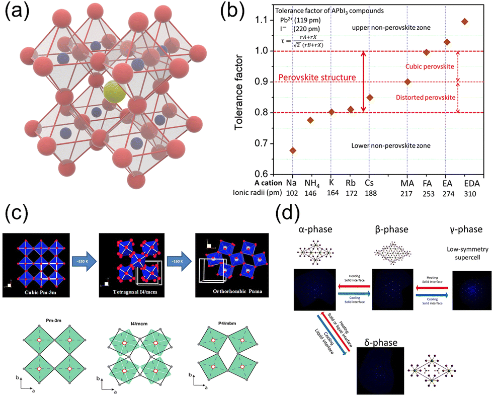 | ||
| Fig. 1 (a) Crystal structure of perovskites. Yellow, blue, and red spheres represent A-site, B-site, and X-site ions, respectively. (b) Calculated tolerance factors for different cations in the lead iodide perovskite system. Reproduced with permission.23 Copyright © 2019, American Chemical Society. (c) The relative rotations of neighboring layers of octahedra along the c-axis. A-site cations are not shown. Reproduced with permission.24 Copyright © 2016, P. S. Whitfield et al. (d) Schematic illustrations of phase transitions in hybrid perovskites. Reproduced with permission.25 Copyright © 2013, American Chemical Society. | ||
To form the framework of 3D perovskite, the essential geometric constraints should be satisfied. The Goldschmidt tolerance factor t and octahedral factor μ were inferred by treating all ions as rigid spheres. The two fundamental parameters can be determined by eqn (1) and (2).
 | (1) |
 | (2) |
![[3 with combining macron]](https://www.rsc.org/images/entities/char_0033_0304.gif) m space group), tetragonal phase (β-phase, I4/mcm space group), and orthorhombic phase (γ-phase, Pnma space group). Phase transition phenomenon is the nature of perovskite materials (Fig. 1c and d).24,25 As the temperature rises, the perovskite can undergo 2 phase transition processes to elevate the symmetry from the initial γ-phase to β-phase and finally reach α-phase. For HOIPs, these two processes occur at 160 K and 330 K, respectively.33 The structural phase transition can significantly alter the perovskites' electronic and optical properties.34
m space group), tetragonal phase (β-phase, I4/mcm space group), and orthorhombic phase (γ-phase, Pnma space group). Phase transition phenomenon is the nature of perovskite materials (Fig. 1c and d).24,25 As the temperature rises, the perovskite can undergo 2 phase transition processes to elevate the symmetry from the initial γ-phase to β-phase and finally reach α-phase. For HOIPs, these two processes occur at 160 K and 330 K, respectively.33 The structural phase transition can significantly alter the perovskites' electronic and optical properties.34
Different types of HOIPs have versatile properties, including semiconductivity, light-emitting properties, dielectricity, ferroelectricity, and mechanical properties due to their structural diversity. Moreover, these properties can be fine-tuned by changing the organic and inorganic components in the perovskite structure. For metal halide perovskite semiconductors, which are principally discussed in this review, the tunable band gaps, long charge carrier lifetime, and high light-absorption efficiency are the critical advantages of FETs.
Although 3D HOIPs exhibit versatile advances, they also have their disadvantages. The instability of the material is one of the biggest issues hindering their application. Unfortunately, HOIPs are sensitive to moisture, oxygen, light, and heat, respectively. For Pb-containing 3D HOIPs, lead can leak out of perovskites, especially in the presence of water, which threatens water quality and human health.35,36 For instance, MAPbI3 can degrade into MAI and PbI2 under moisture. Notably, the preparation of the perovskite utilizes another direction of this reversible reaction. Limiting lead leakage mainly in solar cells has been an emerging topic these past years. Strategies containing encapsulating solar cells and absorbing or recycling Pb2+ have been investigated to deal with the tough issue.37 Encapsulating the device is the most direct approach to limiting lead leakage. Although the encapsulation of solar cells has been widely investigated, it still requires progress to meet the practical demands. For instance, to address the issue of possible damages in outside environments, Jiang et al. employed epoxy resin-based polymers as the encapsulation material, which could heal while heating.38 By adding Pb2+ adsorbents into the device structure, the released toxic ions out of the cell can be effectively reduced. Adsorbents such as polymers, small organic molecules, and metal–organic frameworks can be placed either at both sides of the cell or around the cell since Pb2+ can leak out in every direction.39,40 Adsorbents could also be used to encapsulate the cells and was able to capture 99.9% of leaked Pb2+ without harming the performance.41 To minimize the disposal of the toxic heavy metal as well as reduce the overall cost, solar cells at their end of life are worth-recycling. Versatile approaches have been developed to recycle the device components (mainly PbI2) or make the device easier to recycle, e.g., polar solvent extraction, employing additives, and solvent engineering.42–44 These strategies are promising to overcome the critical toxic metal leakage barrier and can be useful guidelines for HOIPs-based FETs. There is another solution to radically overcome this issue, which is applying lead-free HOIPs. These perovskites can adopt low-dimensional structure, such as (PEA)2SnI4.
2.2. Low-dimensional HOIPs
When the size of the A-site cation is too large for the space between the BX6 octahedra, the octahedra network will be destructed; thus, nonperovskite structures such as low-dimensional layered perovskite will form instead.45,46Low-dimensional HOIPs can be hypothesized as the product of the intercalation of organic layers or the cutting from the bulky ABX3 “parent”.47 Based on the different “cutting” orientations, low-dimensional HOIPs can have different directions such as 〈100〉, 〈110〉, and 〈111〉. In this review, all the mentioned 2D HOIPs belong to the 〈100〉 orientation. Low-dimensional HOIPs can be divided into 2D and quasi-2D segments based on the layer thickness. A 2D perovskite only contains a single octahedra layer, while the quasi-2D counterpart comprises more than one layer of octahedra. Two main phases describing low-dimensional perovskites are the Ruddlesden–Popper (RP) and Dion–Jacobson (DJ) phases, which have the chemical formula L2An−1BnX3n+1 and L′An−1BnX3n+1, respectively. For RP phase perovskites, L represents the bulky monovalent RNH3+ cation, e.g., the aliphatic butylammonium (C4H9NH3+, BA) or Phenethylammonium (C6H5CH2CH2NH3+, PEA). A, B, and X represent small monovalent cations, divalent metal cations, and halide anions, respectively, analogous with conventional 3D HOIPs. However, the DJ phase employs divalent bulky cations instead, mainly [NH3-R-NH3]2+, in which R can also be aliphatic or aromatic. Both the RP phase and DJ phase adopt a sandwich-like geometry as the inorganic component is clamped by adjacent organic layers constituted by L ligands. The integer n represents the number of metal-halide octahedron layers between the bulky L layers. When n = ∞, the 3D ABX3 structure is formed; when n = 1, the L2BX4 monolayer structure is considered to be two-dimensional; when 1 < n < ∞, the “transition phase” quasi-2D structures are obtained. The structures of low-dimensional perovskites are schematically illustrated in Fig. 2a and b.48
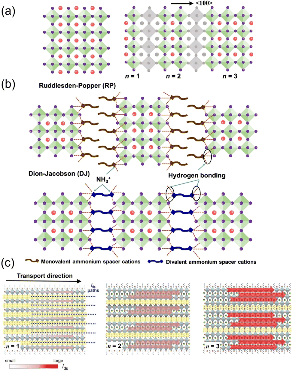 | ||
| Fig. 2 (a) Crystal structure of a 3D perovskite and schematic of cutting the 3D perovskite from the 〈100〉 plane to form the layered perovskites. (b) Crystal structures of RP and DJ phase low-dimensional perovskites (n = 3). Reproduced with permission.48 Copyright © 2022, American Chemical Society. (c) Schematic illustration of the transport behavior of the BA2MAn−1PbnI3n+1 perovskite crystal for n = 1 to n = 3. Red arrows and their corresponding shading indicate the direction of current flow and intensity in the conduction channel, respectively. Reproduced with permission.49 Copyright © 2018, John Wiley & Sons. | ||
Generally, in low-dimensional HOIPs, bulky organic cations are spacers between metal halide octahedra layers. By varying n, the thickness of the inorganic sheet can be modified. Thus, their optical and electronic properties can be fine-tuned. Typically, the bandgap and exciton binding energy are reduced when n increases.50
The alternative organic and inorganic layers form the quantum well (QW) structure, where inorganic and organic layers act as wells and barriers, respectively; thus, unique properties can exhibit.51 For instance, photoluminescence can be enhanced by the suppression of forbidden electronic transition due to their decreased structural symmetry, which makes them suitable for application in light-emission devices.52,53 The significant difference in the dielectric constants (κ) of adjacent organic and inorganic layers brings relatively high exciton binding energies (up to hundreds of meV, while only 45 meV for MAPbI3). This phenomenon is named the dielectric confinement effect in low dimensional systems and was demonstrated to have a critical influence on exciton binding energies.54,55
However, the instability of 3D hybrid perovskites under moisture, oxygen, electron fields, or light illumination has been a challenging issue that researchers must face to commercialize products containing 3D HOIPs.56 Fortunately, the chemical stability of low-dimensional HOIPs is found to be superior to their 3D counterparts. Some researchers suggest that the unstable organic cations lead to the instability of hybrid perovskites. However, for low-dimensional HOIPs, the organic A-site cations are well-protected by highly hydrophobic layers constituted by L.57 Nevertheless, other than the mainly Pb-based 3D HOIPs, most low-dimensional perovskites are Sn-based, and the easy oxidation from Sn2+ to Sn4+ leads to additional air instability to perovskites.
2D HOIPs have individual electron, optical, magnetic, and mechanical properties because of their low dimensional nature.59 For instance, the dielectric confinement, optical nonlinearity, and anisotropic charge transport can be observed from functional 2D HOIPs.60 Excitons in 2D HOIPs are considered as ideal 2D confinement, which has strong confinement in one dimension and free carrier transport in the other two dimensions.60 However, the relatively low mobility and large bandgap are the disadvantages of pure 2D HOIPs compared to 3D, which hinder their applications in electronics. Applying quasi-2D HOIPs may be a promising strategy to overcome the bottleneck.
Quasi-2D HOIPs combine the high optical and electrical properties of 3D perovskites and the improved stability of 2D counterparts. The carrier mobility of quasi-2D HOIPs is superior to 2D counterparts because of the higher ratio of the inorganic backbone (Fig. 2c).49 At the same time, the presence of a hydrophobic organic spacer can prevent the inner parts from harmful moisture, which significantly inhibits spontaneous perovskite degradation.
Although quasi-2D HOIPs provide extra tunability between mobility and stability, the enhanced complexity inevitably increases the difficulty of their preparation, purification, and modification. Specifically, it is not easy to obtain quasi-2D HOIPs pure crystals when n is higher than 5.
2.3. Carrier transport in HOIPs
It has been proved that the organolead trihalide perovskites (APbI3, A represents organic monovalent cations) are direct bandgap semiconductors.62 Theoretical investigations revealed that the cubic phase MAPbI3 has a bandgap of ∼1.7 eV, which consists of its experimental optical bandgap (∼1.6 eV).63 Their outstanding semiconductivity is fundamental for applications in both field-effect transistors and solar cells.We can understand the charge carrier mobility of HOIPs by the Drude model. In Drude's picture, mobility is found to be
 | (3) |
We can also understand charge transport in HOIPs according to their structures. In organic–inorganic hybrid perovskites, the inorganic component forms a strict network through covalent and ionic interactions.18 Charge carriers flow mainly via the inorganic backbone, which agrees with the above conclusion. In this model, organic cations hardly participate in the charge transport process. However, the function of organic cations in HOIPs is still under debate. Many researchers believe that the organic component only has a structural space-filling effect and does not significantly contribute to electronic structure near the Fermi level because of the weak contributions of orbitals of atoms in organic cations. Nevertheless, some investigations in the past few years suggested that the orientation of the organic cation may deform the perovskite structure and thus have the potential for changing the band structure.67,68
 | ||
| Fig. 3 (a) and (b) Hysteresis phenomenon in different perovskite-based electronics. (a) J–V curves of a solar cell. Reproduced with permission.69 Copyright © 2014, American Chemical Society. (b) Transfer curves of a field-effect transistor. Reproduced with permission. Copyright © 2023, Wiley-VCH.71 (c) and (d) Polarization-induced hysteresis in field-effect transistors. (c) Transfer curves of MAPbI3 FET measured at various temperatures between 150 and 250 K. (d) Field-effect mobility as a function of the temperature. Reproduced with permission.72 Copyright © 2015, American Chemical Society. (e) and (f) Schematic illustrations of ionic transport mechanisms in the MAPbI3 perovskite, including (e) the transport of I− and Pb2+ and (f) transport of MA+. Reproduced with permission.73 Copyright © 2015, American Chemical Society. | ||
Ferroelectric behavior was found in some HOIPs. Under bias, hybrid perovskites are found to be slowly polarized, which can alter their electrical behavior (Fig. 3c and d).72 There are high concentrations of defects in perovskites, such as ion vacancies and intervals. The defects on interfaces can act as carrier traps. Good contact between electrodes and perovskites can be achieved once the traps are filled to observe superior device performances. The slow filling and emptying of traps caused the hysteresis. The ion migration describes ion drift under bias, and this process is associated with defects (Fig. 3e and f). For instance, an iodide anion can transfer to an iodide vacancy and remain in another iodide vacancy at its initial location. The activation energies of migration of I−, MA+, and Pb2+ in MAPbI3 were calculated to be 0.58, 0.84, and 2.31 eV, respectively, indicating that iodide anions are the dominating species migrating in MAPbI3.73 Consequently, iodide vacancies (VI) should be mainly focused to inhibit ion migration in MAPbI3. Ion migration was thought to be the dominant factor of hysteresis.73 For FETs, the ionic transport also causes the screening effect. The serious screening effect can result in the inhibition of the actual gate voltage applied on the semiconductor, which significantly reduces the measured mobility. Consequently, mobilities far lower than the theoretical value or even no mobility can be observed in HOIPs-based FETs.70 Moreover, the ion migration can also cause gate pulse-dependent mobility. In the previous work carried out by Pininty et al., mobility could alter approximately three orders of magnitude when gate pulses changed from 5 μs to 10 ms.74
As mentioned above, ion migration is the main barrier to obtaining high-performance perovskite transistors. Moreover, the accumulation of defects that remain by ion migration can also lead to perovskite degradation. To reduce the influence of the ion migration phenomenon, some researchers tested the device properties at low temperatures (approximately 77 K). Labram et al. investigated the temperature-independent electrical characteristics of MAPbI3 thin film FETs. The device showed no field-effect feature at room temperature, but once the temperature decreased below 220 K, the gate voltage-modulated drain current was observed. In addition, higher mobility was achieved at lower temperatures. The temperature-independent phenomena resulted from the drifting ionic species and polarization under gate bias. Also, both of them could be activated by high temperatures.72 Moreover, the carrier diffusion length in the MAPbI3 single crystal was proved to be larger under low temperatures, partly because of the reduced optical phonon scattering.75 Another strategy against ion migration and polarization is applying low-dimensional perovskites due to their quantum and dielectric confinement effects and the less mobile nature of the contained species.72,76,77 For instance, Sn-based 2D or quasi-2D perovskites are promising for low hysteresis devices because of the high activation energy of the dominating Sn2+ vacancies.78 Other parameters, such as the ratio of precursors, have already been demonstrated to inhibit ion migration.79 However, finding a universal strategy to overcome this issue is still challenging.
3. Fabrication methods of HOIPs
This section summarizes versatile fabrication methods for fabricating HOIP films. Facile solution-process ability is one of the advantages of perovskites, whereas most of the published works used this fabrication strategy. However, vapor deposition and other new-type methods have also been applied to obtain high-quality or functional perovskite films. Notably, not all methods mentioned in this section are used to fabricate HOIPs-based FETs. Some strategies developed to process other types of electronics, such as solar cells, are also illustrated because of similar acquirements to obtain high-performance devices, such as the large grain size and smooth surface.3.1. Preparation of polycrystalline perovskite films
The self-organization ability of organic–inorganic perovskites gives the capacity of the facile solution fabrication process of preparing polycrystalline films. To date, most of the reported HOIPs-based electronics have utilized solution-fabricated films.Chemical reactions occur during the CVD process to form perovskites. Due to the controlled growing process of perovskites, the single crystalline film can be observed using CVD. Wang et al. prepared an ultrathin MAPbCl3 single crystal with 10 nm thickness and centimeter size via CVD, where MACl and PbCl2 sources were in the tube simultaneously, as shown in Fig. 4a.84
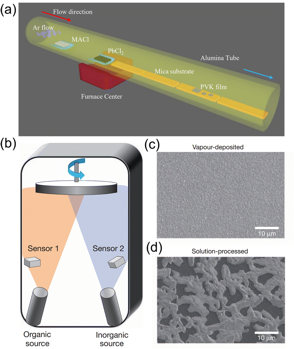 | ||
| Fig. 4 (a) Synthesis of MAPbCl3 by the CVD method. MACl and PbCl2 sources were placed in different places in a single CVD tube. Reproduced with permission.84 Copyright © 2015, American Chemical Society. (b) Schematic illustration of the dual-source thermal evaporation system. (c) and (d) SEM top views of a vapor-deposited perovskite film (c) and a solution-processed perovskite film (d). Reproduced with permission.85 Copyright © 2013, Springer Nature. | ||
Dual-source vapor deposition is an emerging progress of CVD. In dual-source vapor deposition, two kinds of precursors are evaporated, respectively. By the control of sensors, vapor could meet and form the perovskite on the substrate (Fig. 4b). It is obvious that films prepared by dual-source vapor deposition exhibited a much more uniform morphology than the solution-processed films, as shown in Fig. 4c and d. This method is found to be very appropriate for fabricating multilayer structures.85 For instance, Matsushima et al. applied PEAI and SnI2 as organic and inorganic sources, respectively, and a 31-nm-thick (PEA)2SnI4 film was obtained to fabricate a field-effect transistor. Also, they demonstrated that substrate heating while depositing is significant for film quality.86
Niu et al. fabricated near-two-dimensional perovskite solids on different substrates by applying a two-step method. Firstly, the highly crystalline PbI2 nanoplatelets were obtained using physical vapor deposition. The PbI2 nanoplatelets could further convert to perovskites using a CVD system where MAI was applied as the source.87 In conclusion, the (dual source) vapor deposition is a promising method to process uniform perovskite thin films, but the crystallization mechanism is still under debate.80
3.2. Preparation of perovskite crystals
Applying single crystals is advantageous for obtaining improved performance, including higher mobility, uniformity, and enhanced stability due to the reduced structural and ionic defects and free of grain boundaries.88 However, the rigorous conditions to obtain single crystals increased the difficulty of studying them. To the best of our knowledge, most of the perovskite single crystals are prepared via solution processing. | ||
| Fig. 5 (a) Schematic illustration of the growth progress of the 2D (PEA)2PbBr4 perovskite single crystals. (b) Photograph of an as-synthesized transparent, 2 mm (PEA)2PbBr4 single crystal. Reproduced with permission.94 Copyright © 2017, American Chemical Society. (c) Schematic illustration of the patterned growth of regular arrays of perovskite crystals. (d) Optical images of PbI2 seed arrays after the flow seeding process. The scale bars are 40 mm. Reproduced with permission.95 Copyright © 2015, AAAS. | ||
Wang et al. presented a novel method to obtain a perovskite crystal array. Firstly, the PbI2 solution was dropped on a pre-patterned substrate, and PbI2 “seeds” were generated in each hydrophilic region precisely. After exposure to MAI gas under 120 °C, PbI2 microplates could successfully converted into the MAPbI3 perovskite crystal, as shown in Fig. 5c and d.95
An appropriate substrate is essential for epitaxial growth. Substrate materials should be carefully chosen by considering the match of the lattice. For instance, the growth of MAPbI3 on III–V semiconductors, alkali halide, and other materials has already been reported. For example, MAPbI3 has a tetragonal phase with a lattice constant of approximately 6.31 Å. In comparison, KCl also adopts a tetragonal phase with a lattice constant of 6.29 Å, which has only little mismatch.97 The zinc blende GaAs has a lattice constant of 5.65 Å, which are also proper candidates for substrates.98 Quasi-epitaxial growth is a more convenient approach to obtaining the crystalline film, which can be accomplished simply by spin-coating either perovskite or precursors solution on a proper single crystal substrate.96,97
Lei et al. developed a novel lithography-assisted epitaxial growth, whereas a bulk crystal was applied as the substrate, and the patterned polymer was used as a growth mask. Individual crystals grew at first until they got out of the mask. Note that the lattice orientations of the epitaxial crystals were the same. Subsequently, the crystals could grow laterally to form a complete and grain boundaries-free single crystal film and be further transferred to the arbitrary substrate.99 This work revealed the potential of epitaxial growth in fabricating ultrahigh quality single crystal films.
Bulk crystals are sometimes inapplicable for transistors because of the higher thickness compared to carrier diffusion length.88 In this case, epitaxial growth has great potential for fabricating ultrahigh performance thin film transistors. Huo et al. prepared ultrathin CsPbBr3 platelets using van der Waals epitaxy to fabricate field effect transistors.100 Analogous method is also promising for preparing organic–inorganic hybrid perovskite thin-film crystals.
3.3. Supplementary methods
4. Applications of HOIPs in transistors
4.1. HOIPs as channel materials in FETs
The field-effect mobility (μ) is the primary parameter to evaluate a field-effect transistor. The mobility can be determined by either saturation or linear regime data.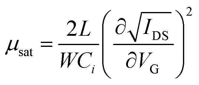 | (4) |
 | (5) |
Moreover, on–off ratio (ION/IOFF), threshold voltage (Vth), and subthreshold swing (SS) are other critical parameters for FETs. The on/off ratio reflects the ability of a transistor to regulate current. The threshold voltage determines the operating voltage of a transistor device. Researchers hope to reduce the threshold voltage to expand the scope of application. In particular, for wearable and implanted electronics, the operating voltage must be under human safety voltage. Subthreshold swing is defined as the derivative of gate voltage with respect to the logarithm of source–drain current. A relatively low SS demonstrates the high sensitivity of output current versus gate voltage, which is favorable for fast response. The following equation can calculate SS.
 | (6) |
The most widely investigated three-dimensional HOIP, MAPbX3, is famous for its balanced ambipolar charge transport. However, not every MAPbI3-based FET can exhibit ambipolar characteristics. Various factors, such as film morphology and electrode material, can affect the carrier transport process.105,106 In unipolar FETs, some employ hole-dominating transportation, which exhibits a p-type character. In contrast, others mainly utilize electrons as carriers, which indicates an n-type transistor.
In this section, perovskite transistors utilizing various components and structures in the past 24 years are summarized. We divided perovskites-channel FETs by polarity. Moreover, transistors employing perovskite dielectrics and novel FETs with functional properties are also exhibited.
 | ||
| Fig. 6 Ambipolar transport characteristic of the perovskite FET at low temperature. Transfer (a) and output (b) characteristics were tested at 78 K. Solid and dashed curves are measured with forward and backward sweeping, respectively. Reproduced with permission.108 Copyright © 2015, Xin Yu Chin et al. | ||
FETs are particularly sensitive to the semiconductor surface because of the critical role of surface charge accumulation and surface transport procedures. Sirringhaus group used MAI to heal ionic defects on the MAPbI3 layer. They developed a cleaning–healing–cleaning (C–I–C) process. The first cleaning was to remove weakly-bonded defective species, followed by exposure to MAI solution. This process aimed to eliminate surface organic-halogen defects and vacancies left or introduced by the first cleaning process. Resident ions were left after healing, which needed the final cleaning. Room temperature mobility of 1.8 and 3.0 cm2 V−1 s−1 for p-type and n-type, as well as decreased hysteresis, were observed in the surface-passivated transistor.110 Zhou et al. passivated grain boundaries in MAPbI3 films using polycaprolactone. Polycaprolactone was found to be confined in grain boundaries. As the polymer ratio increased, the charge transfer characteristic altered from the initial n-type to ambipolar, demonstrating the facilitated hole transfer. Moreover, polycaprolactone could also increase the ion migration activation energy.106
Despite applying different anions, a mixed cation strategy can introduce valuable properties to conventional perovskites. To enhance the device's thermal stability, Yusoff et al. introduced less volatile Cs+ into hybrid perovskites to form triple cation Csx(MA0.17FA0.83)1–xPb(Br0.17I0.83)3. The mobilities for both holes and electrons of >1 cm2 V−1 s−1 could be achieved at room temperature.114
As described in section 3.2, the Duan group fabricated the FETs array based on MAPbI3 crystal grown on pre-patterned electrodes. The FET exhibited ambipolar transport in which the mobility of dominant n-type transportation is ∼2.5 cm2 V−1 s−1 of a backward sweep at 77 K.95
Unlike bulk single crystals (BSCs), thin single crystals (TSCs) have longer carrier lifetimes and higher mobility.121 Yu et al. grew micrometer-TSCs of MAPbX3 using a spatially confined inverse temperature crystallization method. This approach was developed by Saidaminov et al.122 Unlike conventional cooling crystallization methods, the “inverse temperature” means that the solubility of perovskites in some solvents drops as temperature rises. The schematic illustration of the inverse temperature crystallization, and the as-prepared perovskite crystals are shown in Fig. 7. Thus, crystallization can proceed during heating (e.g., MAPbBr3 in DMF). Besides, the lateral size can be fine-tuned, ranging from micrometers to millimeters. By further applying BGBC device configuration, the mobility of hole and electron could reach 4.7 and 2.9 cm2 V−1 s−1, which were superior to those of BGTC devices owing to the reduced distance of the charge pathway to the channel.123
 | ||
| Fig. 7 (a) Schematic illustration of spatially confined inverse temperature crystallization method for producing thin single crystals (TSCs). (b) Fluorescence microscopy images of MAPbI3, MAPbBr3, and MAPbCl3 TSCs, respectively. Reproduced with permission.123 Copyright © 2018, Weili Yu et al. | ||
The reports on perovskites-based ambipolar transistors mentioned in this review are listed in Table 1.
| Channel material | Source/drain | Dielectric | μ h [cm2 V−1 s−1] | I ON/IOFF | μ e [cm2 V−1 s−1] | I ON/IOFF | Ref. |
|---|---|---|---|---|---|---|---|
| a Tested at 78/77 K. | |||||||
| MAPbI3a | Au, Ni | SiO2 | 2.1 × 10⁻² | — | 7.2 × 10⁻² | — | 108 |
| MAPbI3a | Au | SiO2 | 2.5 | ∼106 | — | — | 95 |
| MAPbI3 | Au | Cytop | 1.8 | — | 3.0 | — | 110 |
| MAPbI3−xClx | Au | SiO2 | 7.3 × 10⁻³ | 1 × 10⁴ | 1 × 10⁻² | 1.3 × 10⁴ | 109 |
| MAPbI3−xClx | Au | SiO2 | 10 ± 2.5 | — | 10 ± 3.4 | — | 102 |
| MAPbI3−xClx | Au | Cytop | 1.3 | — | 1.0 | — | 113 |
| Csx(MA0.17FA0.83)1−xPb(Br0.17I0.83)3 | Au | SiO2 | 2.02 | — | 2.39 | — | 114 |
| MAPbI3 | Al | LiF/V2O5 | — | 105 | — | 104 | 125 |
| MAPbI3 | Al/ITO | LiF | — | 104 | — | 104 | 126 |
| MAPbI3 microwires | Au | SiO2 | 7.7 × 10⁻⁴ | 16.7 | 1.8 × 10⁻³ | 11.2 | 124 |
Mixed perovskites. Different properties can be introduced to the mixed metal or halide perovskites. Senanayak proved that the partial replacement of Sn in lead halide perovskites could modify the electronic structure, reduce the hole effective mass, and minimize the screening effects, which benefited hysteresis-free p-type transport.127 Ward et al. changed the surface energy of the Cytop dielectric by the protein. The hydrophobic surface allowed the solution-processed perovskite film directly on the dielectric and enhanced the mobility from 0.23 to 1.3 cm2 V−1 s−1.128 Zhu et al. simultaneously introduced Br and Cl anion into the MASnI3 perovskite. They found that ion migration was not the primary reason for hysteresis in this tin-based perovskite but the deep carrier trap, the vacancies of iodide (VI). In I/Br/Cl perovskite, Br and Cl atoms could fill in and suppress VI, which was consistent with the DFT calculations.129
Single crystals. Wang et al. investigated the electrical reaction that occurs on the interface of Au source/drain electrode and MAPbBr3 single crystal perovskite, which can lead to defects formation. Employing a pentafluorothiophenol (PFBT) buffer layer between Au and perovskite, the maximum hole mobility could reach 15 cm2 V−1 s−1 at 80 K, and the on/off ratio improved by four orders of magnitudes.130
Heterojunctions. Recently, Jo's group reported a type of high-mobility, low-operating voltage “hybrid” transistor by applying a hybrid channel layer and high-dielectric constant dielectric material. The “hybrid” channel consisted of a bilayer of organic semiconductor and perovskite. Conjugated polymers such as P3HT were used to combine with hybrid perovskites. Nketia-Yawson et al. found that compared to the pristine P3HT transistor, the hole mobility could be doubled after injecting an MAPbI3 layer between the P3HT layer and the source/drain electrodes. The enhancement of mobility was attributed to the perovskite-conjugated polymer interactions, such as the passivation of defects on perovskite surfaces.131 Subsequently, they widen the range of perovskites. Hybrid perovskites such as FAPbI3 and FA0.2MA0.8PbI3 were also applied. XPS confirmed the chemical interaction between perovskite and P3HT. Transistors based on FAPbI3/P3HT heterojunction exhibited an ultrahigh mobility of 24.55 cm2 V−1 s−1, which was a consequence of the interaction between perovskite and P3HT, more efficient hole injection, and optimized contact.132 Varying the conjugated polymer also had the potential to elevate the device performance. A remarkable mobility of 30.87 cm2 V−1 s−1 was observed from a Py1/MAPbI3 FET.133 Noticeably, the working voltages of these as-described transistors were relatively low (|Vth| < 2 V), which was the consequence of the high-κ polymer or electrolyte gate dielectrics. These dielectric materials were also responsible for the improved charge densities in the channels and contributed to the high mobilities.
2D HOIPs. Unlike the 3D HOIPs-dominating ambipolar transistors, low-dimensional HOIPs have the potential to be employed in p-type field-effect transistors as well since the first transistor was based on the two-dimensional (PEA)2SnI4.18 Compared to the 3D counterparts, 2D HOIPs always exhibit suppressed ion migration, higher ambient and thermal stability, and mostly p-type transportation.77
Tin-based two-dimensional HOIPs, mainly (PEA)2SnI4, always work as p-type semiconductors. The first HOIP-based FET was fabricated by Kagan et al. in 1999. Spin-coated (PEA)2SnI4 was selected as the channel layer of the p-type TFT, where heavily n-doped silicon wafers with an indium contact and high work function metal were used as gate and source/drain electrodes, respectively. As a result, the p-channel transistor was observed. The field-effect mobility of this organic–inorganic transistor was 0.55 cm2 V−1 s−1, and the on/off ratio was higher than 104, as shown in Fig. 8.18 Employing microcontact printing strategy, transistors with mobility and an on/off ratio of 0.5 cm2 V−1 s−1 and 105 were subsequently achieved, respectively.134
 | ||
| Fig. 8 Structure and properties of the first perovskite-based FET. (a) Schematic illustration of the (PEA)2SnI4 FET. (b) and (c) Output (b) and transfer (c) curves of the transistor. (d) The variation of mobility versus gate voltage. Reproduced with permission.18 Copyright © 1999, AAAS. | ||
Modifications of cations. Mitzi et al. used fluorine-monosubstituted PEA to synthesize the semiconducting (m-FPEA)2SnI4 (m = 2, 3, or 4). The maximum saturation regime field-effect mobility of 2-FPEA, 3-FPEA, and 4-FPEA devices were 0.24, 0.51, and 0.48 cm2 V−1 s−1, respectively. Notably, the corresponding linear regime mobility was about 1 to 2 orders of magnitude lower than the saturation-regime mobilities, which were only 0.003, 0.06, and 0.06 cm2 V−1 s−1, respectively.135 The VG-dependent mobility was observed in both (PEA)2SnI4 and (m-FPEA)2SnI4. Thus, higher mobility was always measured under higher VG. This phenomenon was also observed in other channel materials, such as a-Si and organic semiconductors. The gate-voltage dependent mobility could be explained by the more filled traps and/or the higher carrier density under higher VG.136,137 Methoxy could also be modified in (PEA)2SnI4. The relatively low melting point of the HOIP enabled the melt-processed method. For (4-MeOPEA)2SnI4 and (4-MeOPEA)2SnI4, the saturation and linear regime mobility were 2.6 and 1.7 cm2 V−1 s−1, respectively, with a high on/off ratio up to 106. The improved grain structure associated with the melting process might contribute to enhanced mobility, both in the saturation and linear regime. Note that the μlin was only slightly inferior to the corresponding μsat, which might benefit from the reduced trap density in the melt-processed device.22
Butylammonium (BA) is a classical cation used to research the properties of low-dimensional HOIPs. However, there have been rare reports about BA-based HOIP transistors. Liu et al. fabricated transistors with polycrystalline BA2SnI4 and investigated methods to optimize the film morphology. The highest mobility they observed was 0.03 cm2 V−1 s−1.138 This work demonstrates the potential of aliphatic ligands in charge transport perovskites, but the mobility must be improved to meet the practical acquirement.
Conjugated ligands. Compared to 3D counterparts, low dimensional perovskites weaken the limitations of structural tolerance factors, providing a platform for diverse organic ligands. For instance, people tried to modify PEA to gain better performance. Previous studies have demonstrated the potential of π-conjugated organic cations to alter the band alignment and promote exciton separation in 2D perovskites.139,140 Dou's group first introduced conjugated cation perovskites into transistors by changing the conventional organic cation PEA+ to the highly conjugated cation 4Tm+, where 4Tm+ was a derivative of the thiophene oligomer. The enhanced mobility of the 4Tm2SnI4 transistor is attributed to three aspects: the higher crystallinity and degree of order, larger grains and tolerance of high annealing temperature, and less hole injection barrier from Au electrodes. Surprisingly, not only electrical properties but also stability in conjugated cation perovskites was found to be superior. They suggested that ionic bonding and nonbonded interaction were stronger in 4Tm2SnI4. Their formation energy was calculated to be more negative, which indicated the higher stability.141 A series of conjugated organic ligands was developed, And they are all thiophene-containing groups. The maximum mobility and on/off ratio approached 10 cm2 V−1 s−1 and 106, respectively. The structure and transfer curves of the 2D conjugated ligand perovskite and transistors based on them are shown in Fig. 9.142 Subsequently, they modified 4Tm+ by changing one of the thiophenes rings to the Se-containing selenophen (STM+). However, (STm)2SnI4 had smaller grain sizes than (4Tm)2SnI4, which was not beneficial for high mobility but was suitable for high-efficiency LED devices.143
 | ||
| Fig. 9 Structures and properties of 2D halide perovskites with conjugated ligands. (a)–(c) Chemical structures of the (a) 4Tm, (b) TT, and (c) DTT organic cations. (d)–(f) Transfer curves of FETs based on (d) (4Tm)2SnI4, (e) (TT)2SnI4, and (f) (DTT)2SnI4. Reproduced with permission.142 Copyright © 2021, American Chemical Society. | ||
Optimizations of morphologies and grain sizes. Recently, Wang et al. substituted the phenyl in the PEA+ with thienyl to form a novel cation TEA+. The as-prepared (TEA)2SnI4 films were annealed at different temperatures in the range from room temperature to 160 °C. The authors found that 120 °C was the optimal casting temperature due to the largest grain size. The mobility of the 120 °C casted FET of 1.08 cm2 V−1 s−1 is four times higher than the film fabricated at room temperature.76 Subsequently, pentanoic acid was employed to improve the (TEA)2SnI4 film morphology. A small concentration of pentanoic acid in the precursor solution could alter the nucleation process and suppress tin oxidation.144
Additives in precursor solutions can influence the morphology of the deposited films. Lewis bases were demonstrated to be responsible for controlling the grain size and morphology of perovskite films. In the precursor solution, the electron pairs in the Lewis bases could share with the 5d orbital of lead in PbI2 and form a coordinated compound, hence reducing the Gibbs’ free energy of crystallization to slow the process and further modulate the film morphology.145 Consequently, passivated grain boundaries and larger grain sizes could be formed.146 Zhu et al. found that a 2% volume ratio of urea as an additive of the precursor solution could significantly improve the transistor's mobility and on/off ratio. However, the excess amount of nonversatile urea could harm the device performance.147 Because PbI2 is also the precursor of MAPbI3, Jana found that this strategy was also appropriate for altering MAPbI3 deposition. The addition of diethyl sulfide elevated the MAPbI3 mobility to a surprising 21.41 cm2 V−1 s−1.145
Zhu et al. systematically investigated strategies to optimize (PEA)2SnI4 transistors, especially by improving the film morphology. Excess precursor PEAI was found to be responsible for the self-passivation of carrier traps, and Lewis bases were introduced to enlarge the grain size. Oxygen is usually thought to be fatal to Sn-based perovskites because of the easy oxidation from Sn2+ to Sn4+. Remarkably, the authors also demonstrated that a trace amount of oxygen (∼1 ppm) could enhance the mobility by the p-doping effect.148 Antisolvent strategy was also applied to modulate the film morphology. Unlike the conventional procedure of dripping antisolvent during spin-coating, Zhu et al. directly added antisolvent into the precursor solution, which was also effective but more facile.149
Chao et al. used PEAI/FPEAI (PEA iodide and its fluoro-substituted derivative) to passivate surface defects on (PEA)2SnI4 transistors. The p-doping effect of passivation promoted hole injection. Notably, in FPEAI-passivated devices, F atoms not only elevated the mobility by interacting with perovskites but also could block moisture, significantly enhancing the device stability. Notably, due to the light-harvesting nature of (PEA)2SnI4, the transistor also had the potential for phototransistors. The passivated phototransistors exhibited better photoresponse because of the reduced defects.71
Device architectures. Li et al. fabricated a (PEA)2SnI4 transistor with low operating voltage employing high-dielectric-constant fluorinated copolymer PVDF-TrFE. In the fabrication process, the (PEA)2SnI4 film was directly deposited onto the dielectric layer. However, the solvent used to dissolve the perovskite (DMF) could harm the PVDF-TrFE layer. A 10 nm PTFE buffer layer was introduced to protect PVDF-TrFE from DMF corrosion. Nonetheless, PTFE is a nonpolar polymer, so the polar solvent DMF was hard to disperse on it finely. The perovskite film could possess better morphology if a 20 nm-thick polar CL-PVP layer were prepared on the PVDF-TrFE/PTFE bilayer. CL-PVP (cross-linking poly(4-vinylphenol)) is a hydroxyl-rich polymer demonstrated to modify the surface energy and buffer solvent erosion. The contact angles and film morphology of different dielectric layers are shown in Fig. 10a–f.150 Compared to perovskites on PVDF-TrFE/PTFE, the perovskite films on the trilayer dielectric exhibited enhanced uniformity, as shown in Fig. 10g–j. Although the dielectric constant of PVDF-TrFE/PTFE or PVDF-TrFE/PTFE/CL-PVP was lower than that of pristine PVDF-TrFE, the operating gate voltages of the two devices were still in the low range (−20 to 20 V). However, the improved hysteresis caused by interface charge trapping and a relatively low on/off ratio (∼190) still needs further study (Fig. 10k and l).151
 | ||
| Fig. 10 (a)–(d) Water and CH2I2 contact angles of the UV-ozone treated PVDF-TrFE/PTFE bilayer ((a) and (b)) and PVDF/TrFE/PTFE/CL-PVP trilayer. ((c)–(f)) AFM height and SEM images of the (e) UV-treated PVDF-TrFE/PTFE bilayer and (f) PVDF-TrFE/PTFE/CL-PVP trilayer. (g) and (h) SEM images of the (PEA)2SnI4 thin film on the (g) PVDF-TrFE/PTFE double dielectric layers and (h) PVDF-TrFE/PTFE/CL-PVP triple dielectric layers. (i) and (j) AFM height images of the (PEA)2SnI4 thin film on the (i) PVDF-TrFE/PTFE bilayer and (j) PVDF-TrFE/PTFE/CL-PVP trilayer. (k) and (l) Transfer curves for the (PEA)2SnI4 FETs with the (k) PVDF-TrFE/PTFE bilayer and (l) PVDF-TrFE/PTFE/CL-PVP trilayer. Reproduced with permission.151 Copyright © 2023, American Chemical Society. | ||
Employing the MoOx hole-injection layer (HIL) and top-gate structure can promote hole injection and reduce the trap density. As a result, the HIL-containing FET exhibited hole mobility up to 15 cm2 V−1 s−1 at room temperature.152 Also, using TG/TC and MoOx HIL, Matsushima and coworkers promoted the hole mobility to 26 cm2 V−1 s−1 by increasing the channel length, which might reduce the relative negative effect of contact resistance between the semiconductor and source/drain electrodes. N-Channel FETs were also fabricated by replacing HIL with a C60 electron-injection layer (EIL). Moreover, they found that the surface pretreatment of the substrate with a self-assembled monolayer containing ammonium iodide terminal groups (NH3I–SAM) could induce better perovskite formation during spin-coating.153 MoOx HIL is also applicable for 3D MAPbI3. Tang et al. improved the mobility of the MAPbI3 transistor from 3.55 to 7.47 cm2 V−1 s−1 by inserting the MoO3 layer.154 MoOx was also demonstrated to be compatible with MAPbI3.83
The electron harvesting MoOx can also be applied as a p-dopant. Reo et al. doped (PEA)2SnI4 with MoO3 and TCNQ, respectively. They found that p-doping enhanced the overall hole concentration in perovskite films. Hence, hole traps could be filled, and the excess holes could participate in charge transport.155
Improvements of stability. Lowering the perovskite dimension effectively can bring a significant advance by reducing ion migration due to the confinement effect and thus inhibits the hysteresis. Nonetheless, the hysteresis phenomenon could still be observed in low-dimensional perovskites. Cho et al. passivated iodide vacancies (VI) in (PEA)2SnI4 with S2−, and hysteresis was slightly declined by 10 V. The similar ionic radii of iodide and sulfur ensured the likely access of the latter into VI.156 However, the instability of the tin-based HOIPs in the ambient atmosphere limits its application, mainly because of the easy oxidation from Sn2+ to Sn4+ (p-type doping).157,158 Matsushima et al. systematically investigated the degradation of (PEA)2SnI4, where harmful gaps first form between grains. Optimizing spin-coating solvents and annealing temperature could reduce grain boundary density and therefore slow the degradation.159 Zhang et al. blended (PEA)2SnI4 with aromatic polymer additive poly(4-vinylphenol) (PVP). Hence the morphology, crystallization, stability, and electrical properties were improved due to the interaction between PVP and perovskite.160
Single crystals. After removing the residue layer having rough surfaces of the solution-grown (PEA)2SnI4 single crystal, better contact of electrode and perovskite was obtained by Matsushima et al., and it was necessary to obtain high mobility of 40 and higher. However, the low fabrication yield and bad crystal-substrate contact should be further resolved.58 Shen et al. designed and grew a novel, mixed cation perovskite (PEA)2CsSn2I7 crystals with millimeter size. The introduction of cesium cation was thought to benefit enhanced stability. The single crystal transistor exhibited unipolar p-type transportation, which had a mobility of 33 cm2 V−1 s−1 at 77 K.161
Heterojunctions. Blending 3D perovskites with low dimensional perovskites to form a 2D/3D hybrid is an effective strategy to enhance device performance because 2D parts could regulate the growth of 3D perovskites with improved orientation and crystallinity. Shao added a small amount of quasi-2D (PEA)2FAn−1SnnI3n+1 to FASnI3; consequently, the p-doping levels were reduced, and the crystal quality of FASnI3 was improved. Thus, the mobility was significantly enhanced.162 Yang et al. blended 3D perovskites into 2D perovskites to form a 2D/3D hybrid. Noticeably, the antisolvent dripping strategy was applied to control the growth and crystallinity of the perovskite. The fabricated transistors optimally exhibited hole mobility exceeding 10 cm2 V−1 s−1 and negligible hysteresis.163
Table 2 summarizes HOIP-based p-type transistors with different components.
| Channel material | Source/drain | Dielectric | μ h [cm2 V−1 s−1] | V th [V] | I ON/IOFF | SS [V dec−1] | Ref. |
|---|---|---|---|---|---|---|---|
| a Tested at 100 K. b Tested at 80 K. c Tested at 77 K. | |||||||
| (PEA)2SnI4 | Pd, Pt, or Au | SiO2 | 0.62 | — | >104 | — | 18 |
| (4-FPEA)2SnI4 | Pd | SiO2 | 0.48 | −70 | ∼105 | — | 135 |
| (3-MEOPEA)2SnI4 or (4-MEOPEA)2SnI4 | Au | SiO2/polyimide | 2.6 | — | ∼106 | — | 22 |
| MAPbI3 | Ag | SiO2 | 566 | −3.501 | 2.3 × 10³ | 0.4035 | 82 |
| MAPbI3 | Au | Cytop | 1.3 | — | — | — | 128 |
| MASn(I/Br/Cl)3 | Au | HfO2 | 19.6 | 0 | 3 × 10⁷ | — | 129 |
| MAPbI3/P3HT | Au | P(VDF-TrFE) | 5.01 | 0.74 ± 1.18 | — | −10.76 ± 2.37 | 131 |
| FAPbI3/P3HT | Au | Electrolyte | 24.55 | −0.77 ± 0.09 | >102 | — | 132 |
| MAPbI3/Py1 | Au | Electrolyte | 30.87 | −1.31 ± 0.08 | >104 | — | 133 |
| TEA2SnI4a | Au | SiO2 | 1.8 | 6.6 | >104 | 4.05 | 76 |
| TEA2SnI4a | Au | SiO2 | 2.3 | 9 | 6.1 × 10⁴ | 2.9 | 144 |
| MAPbI3 | Ti/Au | SiO2 | 23.2 | −0.57 | 2.5 × 10⁴ | 0.14 | 145 |
| (PEA)2SnI4 | Au | SiO2 | 0.67 | — | ∼105 | 0.8 | 148 |
| (PEA)2SnI4 | Au | SiO2 | 3.7 | 20 ± 1 | 6.7 × 10⁵ | 1.9 ± 0.2 | 147 |
| (PEA)2SnI4 | Au | SiO2 | 3.8 ± 0.6 | 34 ± 3 | ∼106 | 2.1 ± 0.2 | 149 |
| (PEA)2SnI4 | Au | SiO2 | 2.96 | — | (2.69 ± 1.6) × 104 | −27.5 ± 4.4 | 71 |
| (PEA)2SnI4 | Au | SiO2 | 0.78 ± 0.24 | −1.7 ± 0.3 | (4.4 ± 3.5) × 105 | — | 86 |
| (PEA)2SnI4 | Au | Cytop | 12 ± 1 | −22 ± 2 | (1.9 ± 2.1) × 106 | 0.8 ± 0.1 | 164 |
| (PEA)2SnI4 | Al/MoOx | Cytop | 26 | ∼15 | >106 | ∼1 | 153 |
| MAPbI3 | Au/MoOx | SiO2 | 7.47 | 0.608 | 2.4 × 10⁵ | 0.46 | 154 |
| MAPbI3 | Au/MoOx | Al2O3 | 21.41 | — | 104 | 0.49 | 83 |
| Doped (PEA)2SnI4b | Ni/Au | SiO2 | 100 | — | — | — | 155 |
| (PEA)2SnI4 | Au/MoOx | Cytop | 7.9 ± 2.3 | −54 ± 13 | (2.8 ± 14) × 105 | 5.4 ± 3.1 | 159 |
| (PEA)2SnI4 | Au | PVA/CL-PVP | 0.24 ± 0.05 | 30 ± 6 | ∼5 × 10³ | 8.6 ± 5.0 | 160 |
| MAPbBr3 crystalb | PFBT-modified Au | SiO2 | 15 | — | 106 | — | 130 |
| MAPbCl3 thin crystal | Au | SiO2 | 3.8 | 1.45 | 1.45 × 10⁵ | 2.1 | 123 |
| MAPbBr3 thin crystal | Au | SiO2 | 3.6 | 1.15 | 3.37 × 10⁵ | 1.9 | 123 |
| MAPbI3 thin crystal | Au | SiO2 | 4.7 | 0.16 | 8.78 × 10⁴ | 0.6 | 123 |
| (PEA)2SnI4 crystal | Au/MoOx | SiO2 | 42.1 | −26.8 | 3.6 × 10⁶ | — | 58 |
| (PEA)2CsSn2I7 crystalc | Cr/Au | SiO2 | 34 | — | — | — | 161 |
| (PEA)2FASn2I7/FASnI3 | Au | SiO2 | 0.21 | 2.8 | 104 | — | 162 |
| (4-FPEA)2SnI4/FASnI3 | Au | HfO2 | 11.8 | — | >108 | 0.09 | 163 |
| (PEA)2SnI4 | Au | PVDF-TrFE/PTFE/CL-PVP | 0.42 ± 0.14 | 9.4 ± 2.9 | ∼180 | 5.6 1.8 | 151 |
| (PEA)2SnI4 | Au | SiO2 | 1.45 ± 0.15 | 11.3 ± 1.3 | 2.9 × 10⁵ | 2.6 ± 0.7 | 156 |
| BDASnI4 | Au | PVA/CL-PVP | 0.48 ± 0.05 | 6.60 ± 1.09 | 1.9 × 10⁴ | 6.0 | 165 |
| 4Tm2SnI4 | Au | SiO2 | 2.32 | −20 to −30 | 105 to 106 | ∼10 | 141 |
| TT2SnI4 | Au | SiO2 | 9.35 | −10 to −20 | 105 to 106 | ∼5.4 | 142 |
| BA2SnI4 | Au | PVA/CL-PVP | (1.52 ± 0.63) × 10−2 | 23.6 ± 8.3 | ∼150 | 22 ± 4.7 | 138 |
3D HOIPs. Ngai et al. fabricated MAPbI3 films directly on various gate dielectrics. They found that the surface energy of dielectrics could inversely influence the HOIP crystal sizes and adhesion between the layers. They demonstrated that the larger grains favored growth on a more hydrophobic surface, such as PiPMA and PiBMA. However, perovskites grown on PiPMA and PiBMA also exhibited relatively poor uniformity and adhesion, as shown in Fig. 11. The magnitude of the electron mobility was enhanced by an order of magnitude by optimizing the dielectric material.166 Mativenga et al. observed the abnormal phenomenon that the MAPbI3 film deposited in ambient air had higher mobility than that prepared in the N2 glove box. Before that, moisture was already found to have a possible enhancement to the film morphology by partially dissolving the reactant species during film formation.8 Moreover, oxygen was also responsible for reducing the grain boundaries.167 Works on perovskite films prepared in ambient conditions give us hope to simplify fabrication.
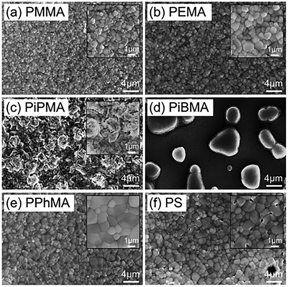 | ||
| Fig. 11 SEM images of various perovskite films synthesized on various polymer substrates: (a) PMMA; (b) PEMA; (c) PiPMA; (d) PiBMA; (e) PPhMA; and (f) PS.166 Copyright © 2017, Royal Society of Chemistry. | ||
By introducing the MAPbI3-ITO Schottky junction, Yu et al. fabricated vertical FETs with an on/off ratio of 104 at room temperature. However, the field-effect mobility was only 0.02 cm2 V−1 s−1.168 Hoang et al. found that doping MAPbI3 with cesium ion could decrease the film roughness and enhance the crystallinity. An electron mobility of 0.04 cm2 V−1 s−1 was observed in this mixed-cation perovskite CsxMA1−xPbI3.169
2D HOIPs. N-Type charge transport has been hardly observed in (PEA)2SnI4, partly because of the huge electron injection barrier between the frequently used Au electrode and (PEA)2SnI4 (1.11 eV). Matsushima et al. employed low work function electrode material (Al and Ag) and C60 electron injection layer and successfully fabricated n-channel transistors with the highest electron mobility of 2.1 cm2 V−1 s−1.170
Single crystals. Li et al. investigated the effect of n in the RP phase perovskite (BA)2MAn−1PbnI3n+1. Transistors were fabricated using single-crystal flakes exfoliated form crystals prepared by the SECT technique.89 All transistors exhibited n-type conduction when n = 1, 2, and 3. Considering the existence of hysteresis, the field-effect mobilities were calculated to be 1.1 × 10⁻³, 7 × 10⁻², and 9.5 × 10⁻¹ cm2 V−1 s−1, respectively, for n = 1, 2, and 3 using the data of backward sweeping direction at 77 K, which proved that mobilities could be enhanced by increasing the n.49 Liu et al. also studied transistors based on the BA2MAn−1PbnI3n+1 crystal. They supposed that the device was a Schottky-barrier type FET with an n-channel. The conduction band would bend when the gate voltage increased, and electrons had enhanced charge injection. The device showed a mobility of 0.087 cm2 V−1 s−1 under 150 K. However, the reason why the mobility of the BA2MAn−1PbnI3n+1 single crystal was in the low range even at low temperatures was still unclear.171
Different types of n-type perovskite FETs are listed in Table 3.
| Channel material | Source/drain | Dielectric | μ e [cm2 V−1 s−1] | V th [V] | I ON/IOFF | SS [V dec−1] | Ref. |
|---|---|---|---|---|---|---|---|
| a Tested at 150 K. | |||||||
| MAPbI3 | Au | PPhMA | 0.4 | 34.3 | 5.1 × 10⁵ | — | 166 |
| MAPbI3 | IZO | AlOx | 0.2 | — | — | 0.04 | 167 |
| MAPbI3 | ITO/Al | HfO2 | — | — | 104 | 1.1 | 168 |
| CsxMA1−xPbI3 | IZO | AlOx | 0.04 | 8.5 | — | 0.03 | 169 |
| (PEA)2SnI4 | Al/C60 | Cytop | 2.1 | 47 ± 4 | (2.4 ± 6.4) ×104 | 1.1 ± 0.2 | 170 |
| (PEA)2SnI4 | Al/C60 | Cytop | 4.7 | ∼15 | >104 | ∼1 | 153 |
| (PEA)2SnI4 crystals | Al/C60 | SiO2 | 121 | 30.8 | 6.3 × 10⁶ | 0.38 | 58 |
| BA2MAn−1PbnI3n+1 single crystala | Au | SiO2 | 0.087 | — | 106 | — | 171 |
4.2. HOIPs applied in functional FETs
In this section, four types of functional FETs are presented, which are phototransistors, memory transistors, artificial synapses, and light-emitting transistors. In functional field-effect transistors, hybrid perovskites can play multiple roles, such as carrier transport, light absorbing, and charge trapping. HOIPs can also combine with other materials with versatile properties to integrate the merits of both the components. | (7) |
In the above equation, IPhoto and IDark are drain currents under light illumination and in the dark, respectively. PIn is the total power of incident light, and A represents the device area.
D* has a linear dependence on A and bandwidth (Δf) and is inversely related to the noise equivalent power (NEP). D* represents the detect ability of low-intensity incident light, which refers to the minimum detectable light intensity. In cases of shot noise limit, D* can be calculated by the following equation:
 | (8) |
In phototransistors, the incident light can regulate the output current like the typical gate bias, which is called the photogating effect. In other words, light serves as the additional gate voltage. Hybrid organic–inorganic perovskites are semiconductors with direct and tunable bandgap, where Wannier excitons with small binding energy generate. Those merits make HOIPs appropriate as the light-absorbing layer in PTs.
HOIPs can serve the function of light absorption, exciton separation, and charge transport simultaneously. That leads to the possibility of phototransistors with single perovskite active layers. Li et al. early fabricated MAPbI3 and MAPbI3−xClx-based PTs applying bottom-gate top-contact (BGTC) configuration (Fig. 12a). The devices exhibited balanced ambipolar transportation, excellent photoresponsivity, and high response speed. As shown in Fig. 12b, the dark currents of this device approached 0 V even under high gate and source–drain voltages. However, IDS could fast switch to high value after exposure to light. The R values of 320 and 47 A W−1 were calculated for PTs based on MAPbI3 and MAPbI3−xClx, respectively. The relatively lower responsivity was attributed to higher dark currents in mixed halide perovskites. In addition, another vital parameter, the photoconductive gain (G), which represents the number of charge carriers induced by a single incident photon, was estimated as 10–100 of the PTs.172
 | ||
| Fig. 12 (a) Schematic structure illustration of the phototransistor with an MAPbI3 channel. (b) Photocurrent responses of the phototransistors on light illumination, showing time-dependent photosensitivity with a time interval of 0.5 s at VGS = −30 V and VDS = −30 V. Reproduced with permission.172 Copyright © 2015, Feng Li et al. | ||
Facile preparation is a prominent advantage for HOIPs-based PTs compared to conventional devices applying inorganic semiconductors. The HOIP light-absorbing layer can be easily solution-processed, even in the ambient atmosphere.176 He et al. demonstrated the all-solution-processed PTs using sol–gel SiO2 gate dielectric. The dielectric layer was also responsible for protecting the active layer.177
2D HOIPs contain highly hydrophobic organic spacers, thus have enhanced air and moisture stability compared to their 3D counterparts. Chen et al. first fabricated 2D HOIP (PEA)2SnI4-based PTs with an ultrahigh photoresponse of 1.9 × 10⁴ A W−1.178 Wang and coworkers introduced ferroelectric polymer poly(vinylidene fluoride-trifluoroethylene) (P(VDF-TrFE)) as dielectric material in (PEA)2SnI4 PTs. Charge traps were suppressed by the special dielectric layer, which led to inhibited hysteresis. Particularly, the ferroelectric polymer could exhibit different states under different gate biases. Holes could accumulate in the channel layer, causing a higher drain current at the “down” state and vice versa.179 Recently, 3D/2D layer heterojunction was demonstrated to combine the advantages of both components. This strategy could effectively improve the ambient stability of 3D perovskite without sacrificing its photoelectric properties.180 PTs with different device architecture has also been investigated. Xie et al. vertical FETs using MXene (Ti3C2Tx) nanosheets as the source electrode. The detectivity was relatively high (7.84 × 10¹⁵ Jones), indicating the potential of vertical architecture and MXene electrode in phototransistors.181 Nonetheless, intrinsic Sn vacancies, the oxidation from Sn2+ to Sn4+ (i.e., self p-doping), and unipolar p-type transportation character may limit the development of low-dimensional, tin-based perovskite phototransistors.
HOIPs exhibit excellent light-absorption properties, however, compared to inorganic semiconductors, the mobilities and gate modulation of pristine HOIPs-based PTs are still relatively low, which limits their overall performances, including R and response speed.6 To enhance carrier mobilities of PTs, a heterojunction structure was introduced by combining perovskites with high mobility materials (e.g., graphene182,183 or carbon nanotubes184,185), and the overall photodetecting performance could be elevated.186 By fine-tuning the band alignment, the junction configuration can promote the exciton separation and charge transport processes. In such devices, HOIPs mainly played a light-absorbing role, and conventional materials dominated carrier transportation.
Layer heterojunctions. Lee et al. designed enhanced performance hybrid PTs consisting of MAPbI3-graphene bilayer.182 Ultrahigh R and D* were obtained by sequentially introducing the vapor deposition of graphene and MAPbI3.183 Du et al. fabricated PTs-containing MAPbI3 capping indium gallium zinc oxide (IGZO) channel layer. IGZO was thought to be an attractive channel material having an n-type mobility of 12.4 cm2 V−1 s−1. The perovskite-capped IGZO PTs showed an undescended mobility of 12.9 cm2 V−1 s−1, as well as a fair R of 106 A W−1 and D* of 9.5 × 10⁹ Jones.187 For low-dimensional perovskites with enhanced stability, Shao demonstrated RP phase (BA)2MAn−1PbnI3n+1 with either faster response or enhanced stability.188 The layer heterojunction structures combined high mobility and excellent light absorption property of different materials. In addition, Li et al. demonstrated that a 40 nm thick PbI2 layer between the perovskite layer and adjacent dielectric layer could effectively reduce the charge recombination at the interface, mainly because the PbI2 simultaneously acted as the barrier of holes and electrons in the perovskite.189
Bulk heterojunctions. Li and coworkers fabricated PTs using the single-wall carbon nanotubes (SWCNTs)-embedded MAPbI3−xClx film, which exhibited ultrahigh field-effect mobilities of 595.3 and 108.7 cm2 V−1 s−1 for holes and electrons under light illumination, respectively. The record-high mobilities led to a high responsivity of 1 × 10⁴ A W−1 and G over 8 × 103.185 In some device structures, HOIPs were not continuous. For instance, in the work by Wang et al., perovskite “islands” were grown onto graphene, and ultrahigh R and G of approximately 6.0 × 10⁵ A W−1 and 2.01 × 10⁹ were achieved because of the photogating effect, respectively. Specifically, after the separation of excitons at the interface between perovskite islands and graphene, trapped electrons in the perovskites caused the photogating effect while holes were free to transfer to graphene.190 In PTs demonstrated by Xu and coworkers, MAPbI3 nanoparticles (NPs) were induced to the surfaces of organic semiconductor 2,7-dioctyl[1]-benzothieno[3,2-b][1]benzothiophene (C8-BTBT) single crystal array to broaden the spectral response. High G was estimated to be 9 × 10⁴ for their phototransistors. The integration of two kinds of semiconductors gave the PT dual-band detectivity, in which excitons are generated in MAPbI3 NPs under visible light and in C8-BTBT under UV irritation. In both situations, electrons were trapped in C8-BTBT, and holes made a contribution to the enhanced photocurrent.191 Zhu et al. prepared (PEA)2SnI4/conjugated polymer-wrapped semiconducting carbon nanotubes (semi-CNTs) blend as the active layer. They observed that film pinholes, gaps, and charge traps were lower in the mixed film, indicating a great blend of perovskites and semi-CNTs. The mobility enhancement was due to the improved morphology and addition of highly conductive CNTs.192 Chen et al. prepared MAPbI3 nanowires using a silicon nanowire template. The as-synthesized nanowires were combined with organic semiconductors (p-type PDVT-10 or n-type N2200) to form heterojunctions.193 In short, the integration of perovskites and conventional semiconductors can combine the merits of both components: the effective photoresponse of perovskites and gate modulation of semiconductors. However, introducing charge-transporting materials inevitably increased the preparation difficulties and total costs.
Notably, the performances of some perovskites-based PTs can be significantly influenced by gate bias. Liu and coworkers demonstrated that in their 2D perovskites-based Schottky-barrier PT, R could alter from 0.0053 A W−1 at VG = 0 V to 1.29 A W−1 at VG = 100 V, which increased by over two orders of magnitude. This phenomenon could be explained by the working principle that at low gate voltage under threshold voltage (VG < 40 V), the Schottky barrier dominated the device current, and the photogenerated carriers could not only improve the channel carrier concentration but also promote charge injection. In this case, the photocurrent had a linear relationship with light intensity, i.e., R remained constant. But at a high VG of > 60 V, photoinduced charges could only influence channel conductivity, and the relation between ID and PIn became nonlinear.171
The properties of various HOIPs-based phototransistors are listed in Table 4. Note that some of the PTs are ambipolar transistors, and their mobilities for holes and electrons are exhibited as μh/μe.
| Active materials | R [A W−1] | D* [Jones] | μ FE [cm2 V−1 s−1] | Ref. |
|---|---|---|---|---|
| MAPbI3 | 320 | — | 0.18/0.17 | 172 |
| MAPbI3−xClx | 47 | — | 1.24/1.01 | 172 |
| MAPbI3 | 8.95 | 2.9 × 10¹² | — | 194 |
| MAPbI3 | 10.72 | 6.2 × 10¹³ | — | 177 |
| MAPbI3 | 0.62 | 6.87 × 10¹⁵ | (5 ± 4) × 10−4/(4 ± 3) × 10−2 | 176 |
| MAPbI3 | 1.4 × 10⁻² | — | 1.7 | 6 |
| MAPbI3−xClx | 32 | 8.94 × 10¹¹ | 2.32/1.18 | 101 |
| (PEA)2SnI4 | 1.9 × 10⁴ | — | 0.76–1.2 | 178 |
| (PEA)2SnI4 | 14.57 | 1.74 × 10¹² | 0.04 | 179 |
| (PEA)2SnI4 | 8.8 × 10⁵ | 1.5 × 10¹⁷ | 3.7 | 147 |
| (PEA)2SnI4 | 2.1 × 10³ | 7.84 × 10¹⁵ | — | 181 |
| MAPbI3-graphene bilayer | 1.73 × 10⁷ | 2 × 10¹⁵ | 212/141 | 183 |
| MAPbI3-IGZO bilayer | 2.5 × 10⁻² | 9.5 × 10⁸ | 12.9 | 187 |
| (BA)2MAn−1PbnI3n+1-graphene bilayer | 105 | 3.3 × 10¹⁰ | — | 188 |
| (FAPbI3)1−x(MAPbBr3)x/PbI2 | 1302 | — | 21.36/49.32 | 189 |
| (PEA)2MA2Pb3I8-SWCNTs bilayer | 2.0 × 10⁶ | 7.1 × 10¹⁴ | 9.7 | 184 |
| SWCNTs-embedded MAPbI3−xClx | 1 × 10⁴ | 3.7 × 10¹⁴ | 595.3/108.7 | 185 |
| MAPbI3-coated C8-BTBT single crystal | >1.72 × 10⁴ | 2.09 × 10¹² | 1.13 | 191 |
| (PEA)2SnI4/semi-CNTs | 6.3 × 10⁴ | 1.12 × 10¹⁷ | 1.51 | 192 |
| MAPbI3 nanowire/PDVT-10 | 169 | 6.7 × 10¹¹ | 0.18 | 193 |
| MAPbI3 nanowire/N2200 | 18 | 3.5 × 10¹¹ | 0.21 | 193 |
Generally, memory transistors include ferroelectric type transistors and charge-trapping type transistors.198,201 In ferroelectric-type FETs (FeFETs), ferroelectric materials are used as gate insulators to modulate the channel charge concentration under gate voltages. The ferroelectricity of perovskite-structured materials such as BaTiO3, PbZrxTi1−xO3, and SrBi2Ta2O9 were discovered in the early years. Mathews and coworkers first demonstrated ferroelectric memory transistors based on inorganic perovskites in 1997. In their FeFETs, La0.2Ca0.3MnO3 and PbZr0.2Ti0.8O3 were used as channel and gate dielectric, respectively.202 However, the thickness of the perovskite films should be downscaled to match the demand of high memory windows, but it is challenging, especially in commercial fields. Moreover, the high dielectric constants of perovskite materials also lead to unreliable polarization.203,204 As a result, the emerging HOIPs-based memory transistors have been more likely to based on the charge-trapping mechanism. In charge-trapping transistors, charge carriers will be captured powerfully under programming gate bias. For instance, in the widely-investigated floating-gate transistor (a type of charge-trapping transistor), a floating-gate layer is sandwiched between two dielectric layers, namely, tunnelling and blocking layers.195,199 When a significant enough programming bias is applied, charges in the channel layer can transfer across the tunnelling dielectric and be captured by the floating-gate layer. Charges trapped in the floating-gate layer are not able to return to the channel layer even if the bias is cancelled due to the existence of the barrier. This causes a shift in the threshold voltage, which can be read repeatedly to realize the nonvoltaic memory. In the erasing process, the opposite bias is applied. Thus, the trapped carriers can be released, and the threshold voltage can return. The additional evaluation parameters of a memory transistor versus an ordinary FET include the memory window, retention time, and write-read-erase-read (WRER) endurance. The difference between the initial state (OFF state) and programmed state (ON state) is defined as the memory window (ΔVth). A large ΔVth is responsible for the distinct difference between working states and potential multilevel memory. The retention time describes the device ability to maintain an ON state after programming. WRER cycles reflect the device stability during the repeating working process. Obviously, the longer retention time and immense WRER endurance are more desirable for high-performance memory devices.
Floating-gate memory transistors can be simply fabricated by inserting the required layers into normal FET structures. Vasilpoulou et al. achieved transistor flash memory by adding a nanofloating-gate layer between the perovskite semiconductor layer and gate insulator. The nanofloating-gate consisted of a star-shaped copolymer composed of styrene and fluorene (termed as P(S–F)4) and fullerene derivative PC61BM. The insulating styrene acted as a tunnelling dielectric, while the fluorene and PC61BM acted as the floating-gate. PC61BM could effectively capture electrons during the writing process. The trapped electrons generated an internal electric field to help holes accumulate in the perovskite channel, hence reducing the threshold voltage. This flash memory transistor exhibited a short programming/erasing time of 50 ms, a satisfactory memory window of 30 V, and a long retention time of 106 s.205
HOIPs themselves are potential candidates for charge-trapping materials due to their abundant trap states and unique energy band structure. In particular, 2D HOIPs have a unique quantum-well structure, which benefits the charge-trapping process. Gedda et al. fabricated memory transistors based on the (PEA)2SnI4-C8-BTBT blend. In the negative biasing condition, holes were injected into the PbBr4 quantum well and unable to escape unless adequate positive gate voltage was applied. In such a device, the perovskite layer acted as a floating-gate. Surprisingly, the mix of organic semiconductors and perovskites could regulate the crystallization of perovskites.206
Jiang et al. first demonstrated perovskite nanocrystals (NCs)-based transistor memory. MAPbBr3 NCs-decorated CdS nanoribbons (NRs) were applied to fabricate the nanofloating-gate transistor (Fig. 13a). Fig. 13b shows memory windows under different gate bias ranges. A larger memory window was achieved under a larger gate voltage, indicating the charge-trapping mechanism. At positive erasing bias, the electron density was elevated in the CdS NR channel, followed by the injection into MAPbBr3 NCs via Fowler–Nordheim tunnelling. This erasing process could turn the transistor into an OFF state. On the contrary, the positive VG could release the trapped electrons and “turn on” the device. Fig. 13c shows the band alignment of different modes for the transistor. This nanofloating-gate memory transistor exhibited excellent memory performance, including a memory window of 77.4 V, high on/off ratio of >7 × 10⁷, long retention time of 12000 s, and ambient stability of 50 days.207
 | ||
| Fig. 13 (a) Schematic device structure of MAPbBr3 NCs/CdS NR memory transistor. (b) Electrical transfer characteristics at VDS = 1 V of the device recorded after every sweeping cycle. (c) Energy band diagrams of the device during the charge storage process. Reproduced with permission.207 Copyright © 2019, American Chemical Society. | ||
Benefiting from the hysteresis caused by an ionic defect and ion migration, metal halide perovskites have the potential to be the single active material in memory devices.197,208,209 Park and Lee first introduced Dion–Jacobson (DJ)-phase HOIPs into memory transistors. 3AMP)PbI4 (3AMP = 3-(aminomethyl)piperidinium)) was chosen as the active layer material. The authors found that the ratio of DMF and DMSO in the spin-coat solution could affect the grain sizes of perovskites, and the larger grain sizes benefited from an enhanced on/off ratio. Consequently, the as-described memory FETs exhibited reliable resistive switching behavior with data retention (103 s) and WRER endurance (103 cycles). Moreover, DJ-phase HOIPs have enhanced stability compared to RP-phase counterparts because there are no van der Waals gaps between adjacent layers, which is vital for memory devices.208 Haque and Mativenga realized the MAPbI3 memory transistor and carefully investigated the ion migration in the perovskite. The ion migration (mostly the migration of I−) by the drive of source–drain voltage caused the ions' dynamic redistribution and the switching from a high resistance state (HRS) to a low resistance state (LRS). The retention time and endurance were tested to be >104 s and >103 cycles, respectively.209 These works inspire us that although, in most cases, the hysteresis phenomenon is harmful to perovskites’ application in FETs, it can also be exploited to exhibit unique properties.
Photomemory FETs. Benefiting from the admirable light-absorbing capacity and intrinsic charge-trapping ability, HOIPs are promising for fabricating photomemory transistors, which have the dual function of photodetection and memory. Chen's group systematically investigated a specific device architecture similar to floating-gate transistors, which is an additional hybrid layer consisting of perovskites and polymer matrix inserted between the channel layer and gate dielectric, which plays the role of light-absorption and floating-gate simultaneously, as shown in Fig. 14a. They fabricated a multilayered phototransistor with a pentacene channel layer and a light-sensitive composite layer composed of a polystyrene (PS) matrix with dispersed MAPbBr3 nanoparticles (NCs). In the photoprogramming process, electrons in pentacene would transfer to perovskite NCs to fill the vacancies resulting from exciton formation and got trapped until the erasing voltage was applied. The proposed device mechanism is schematically illustrated in Fig. 14b. This device could maintain reliable memory for more than three months and had an on/off ratio of >104.210 Furthermore, the impact of altering the matrix polymer was investigated by Ercan et al., who revealed that different polymers could cause different sizes of perovskite NPs and film morphology due to the coordination between oxygen atoms of polymer and lead atoms of perovskites. In this study, the PS matrix was found to be superior to poly(4-vinylphenol) (PVPh), PMMA, and PMAA.200 This work confirmed that the aggregation of perovskite NPs was detrimental to memory performance, which was in agreement with the previous work.210 However, further study demonstrated that changing PS to poly(2-vinylpyridine) (P2VP) could help boost the device performance. The P2VP-based photomemory transistors exhibited an enhanced on/off ratio (105) and lower light illumination requirement.211
 | ||
| Fig. 14 (a) Schematic device configuration of the PS with dispersed MAPbBr3 NCs photomemory with the SEM and TEM images of the MAPbBr3/PS composite film. (b) The operating mechanism of the nonvolatile perovskite-based photomemory. Reproduced with permission.210 Copyright © 2017, John Wiley & Sons. | ||
Self-assembled block copolymers can exhibit natural phase separation and form well-organized microstructures. The block copolymer polystyrene-block-poly(ethylene oxide) (PS-b-PEO) was blended with MAPbBr3, and solution-processed light-absorbing polymer P3HT was introduced as a channel layer to broaden the device absorption spectra by Chen's group. In the device, excitons could form in either P3HT (under red light illumination) or perovskite (under green or blue light illumination). These two situations had the same consequence to electrons trapped in perovskites (Fig. 15a–f).212 PS-b-PEO could also combine with quasi-2D and 2D perovskites. Interestingly, by adding a small amount of PEABr into the FAPbBr3 solution, the 3D perovskite would turn into a quasi-2D phase, and the crystal orientation could be significantly improved.213 Recently, biphenylmethylammonium lead bromide ((BPMA)2PbBr4) with room temperature phosphorescence (RTP) was introduced to this type of device by Chen and coworkers. Compared to PEA, BPMA had a larger conjugated system and thus smaller triplet exciton energy. As a result, triplet–triplet Dexter energy transfer (TTDET) was allowed in (BPMA)2PbBr4 but inhibited in (PEA)2PbBr4. The formation of triplet excitons with longer lifetimes enabled high photoresponsivity and low power consumption (Fig. 15g and h).214
 | ||
| Fig. 15 (a) and (b) TEM images of (a) BCP-1/MAPbBr3 and (b) BCP-2/MAPbBr3 composite films after annealing for 17 h in benzene vapor. (c) and (d) GIWAXS 2D pattern of (c) BCP-1/MAPbBr3 and (d) BCP-2/MAPbBr3 composite films. (e) and (f) The GISAXS profiles of (e) BCP-1/MAPbBr3 and (f) BCP-2/MAPbBr3 composite films. Reproduced with permission.212 Copyright © 2020 John Wiley & Sons. (g) and (h) The schematic diagram of the operating mechanism of (g) BCP/(PEA)2PbBr4 and (h) BCP/(BPMA)2PbBr4-derived photomemory. Reproduced with permission.214 Copyright © 2023 Jian-Cheng Chen et al. Advanced Science published by Wiley-VCH GmbH. | ||
The integration of HOIPs and other semiconductors can broaden the overall absorption spectrum of the device, thus widening the detection range. This property is also well-matched with the multibit memory characteristic. Yang et al. selected the photosensitive n-type semiconductor BPE-PTCDI as the channel material, which had complementary absorption spectra with perovskites. The device could be photowritten under light with three wavelengths of 650, 530, and 405 nm. Interestingly, the memory could be erased under 254 nm UV irritation without gate bias.215 Lai and coworkers investigated photomemory FETs based on MoS2/hBN/(BA)2MAPb4I7 nanosheets van der Waals heterojunctions, in which MoS2, hBN, and perovskites were channel, tunnelling dielectric, and floating-gate materials, respectively. The high-quality perovskite nanosheets exfoliated from single crystals also played the role of light-absorption. Specifically, MoS2 had absorption peaks at 627 and 680 nm, whereas perovskites had 570 nm absorption. The device exhibited no memory behavior in dark but controllable memory windows (with the highest value of 94 V) under light illumination.216 In their subsequent work, the perovskite (BA)2MAPb4I7 was demonstrated to have the p-type doping effect, which changed the polarity of MoS2 from n-type to p-type. Moreover, the MoS2/perovskite heterojunction had a broadband absorption and thus high-performance (with a memory window of 104 V as well as fast writing speed of 20 μs), multibit (100 states, >6 bits) optoelectronic memory with a wide range operating wavelength of 405–1550 nm could be realized.217 In conclusion, photomemory transistor combines the advantages of different materials (e.g., perovskites, organic semiconductors, and polymers), and the properties can be promoted by optimizing the components, device architecture, and film morphology.
Due to the versatile characteristics of artificial synapses, the synaptic plasticity is vital for application. To understand plasticity, we should first comprehend the postsynaptic current (PSC). PSC is the output current of a synapse after stimulation. The changing behavior of PSC after stimuli is called plasticity. Plasticity includes short-term plasticity (STP) and long-term plasticity (LTP). STP occurs when a single pulse is applied to the device, and the output current will not return to the initial value suddenly after the pulse. However, this phenomenon usually maintains only about a few minutes or seconds. Interestingly, under periodicity-repeated stimuli, the later pulse will cause a larger current than the previous one. The ratio of the two currents is defined as paired-pulse facilitation (PPF). STP may convert to LTP by enough repeated stimuli and can last for a more extended period of time. This process is also called “consolidation”.
Artificial visual systems converting and remembering light signals have broad applications in image identification, the Internet of Things (IoTs), and robots.223 Over the past few years, different device architectures were developed to mimic animal visual synapses, mainly including two-terminal photoconductors and three-terminal phototransistors,218,224 in which phototransistors with signal amplification and ionic-to-electronic transduction properties were regarded as the promising device structure.220 Metal halide perovskites, including inorganic perovskites and HOIPs, are suitable materials for artificial synapses owing to their excellent optoelectronic properties and facile fabrication process. Moreover, HOIPs exhibit the intrinsic hysteresis phenomenon because of ion migration, charge trapping, and ferroelectric polarization, which is appropriate to stimulate the STP and LTP behavior.219 Notably, perovskites usually play the light-absorbing role rather than charge transport in photosensitive synaptic transistors.
Qian et al. revealed that the charge trapping mechanism could explain the STP and LTP character of the (PEA)2SnI4-based transistor-structured artificial synapses, where the deep-trapped electrons generated by previous light illumination could induce more holes at the second pulse. Specifically, the dominating electron traps were Sn vacancies.225 Sun and coworkers fabricated perovskite artificial synapses employing (PEA)2SnI4 as the single active material. STP, as well as LTP, were successfully observed, as shown in Fig. 16, which shows a typical STP behavior, where the PSC quickly returned to the initial state after a few seconds. Fig. 16d and e demonstrate that continuous stimuli with a frequency of 1 Hz were not able to convert STP to LTP, but the conversion could be achieved when the frequency was enhanced to 20 Hz. It is obvious that the declining speed of STM was much higher than that of LTM. The plasticity was attributed to abundant traps in or onto the perovskite films. The more the pulses applied to the device, the more opportunities the carriers had to be captured by deeper traps, which needed a longer time to release.219 Although single-component perovskite transistors could successfully exhibit synaptic characters, however, the device performance can be further improved and fine-tuned employing heterojunction structures.226
 | ||
| Fig. 16 (a) Schematic illustration of a biological synapse and the signal transmission process. The top right corner is an illustration of a synaptic transistor. (b) The UV-vis absorption spectrum of a (PEA)2SnI4 film (red line) and photocurrents of the (PEA)2SnI4-based photoconductor under 470, 590, and 660 nm illumination at the same intensity of 5 μW cm−2 (blue stars). (c) Cross-sectional illustration of the artificial synaptic transistor. The insets are examples of the input light pulses and PSC. (d) ΔPSC triggered by a light pulse under a gate bias (VG) of 2 V, which is the STP behavior. (e) STP (duration = 20 ms, frequency = 1 Hz) and (f) LTP (duration = 20 ms, frequency = 20 Hz) behaviors triggered by light pulses.219 Copyright © 2019, John Wiley & Sons. | ||
Layer heterojunctions. Park et al. demonstrated the bilayer structure of transparent inorganic semiconductor indium zinc tin oxide (IGTO) and the HOIP (BA)2PbBr4, which significantly enhanced the retention time of plasticity compared to pristine (BA)2PbBr4. It can be inferred that 2D perovskites may be more favorable in artificial visual synapses because the BA-based 2D perovskite has deeper level defects compared to its 3D counterparts, leading to a longer retention time.227 Huang et al. combined (PEA)2SnI4 and Y6 with complementary absorption spectra to broaden the detection range. Owing to the ambipolar transporting behavior of the (PEA)2SnI4/Y6 hybrid film, the device could distinguish different colors by different ΔPSC (negative ΔPSC for visible and positive ΔPSC for NIR light). As a result, the heterojunction device had the ability to recognize and remember different colors varying from visible to NIR light.223
The 3D MAPbI3 is also an appropriate material in visual synapses due to its outstanding light-harvesting property. Hsu et al. demonstrated a red-light-stimulated synapse transistor with the P3HT channel layer and the polystyrene-block-poly(ethylene oxide) (BCP)/MAPbBr3 heterojunction light-harvesting and floating-gate layer. However, limited by the exciton length, the thickness of the P3HT layer was strictly limited. The device performance was significantly influenced by the thickness of the P3HT layer controlled by rotation speed while spin coating.228 For lead-based 3D perovskites, the high toxicity of lead is not suitable for broad applications. Recently, aiming to reduce the toxicity of lead-based perovskites, Jeon et al. fabricated artificial synapses using a novel mixed-metal perovskite, where 90% of the lead ions were substituted by manganese ions. This work demonstrated the potential of ecofriendly perovskites in optoelectronic devices.229
Bulk heterojunctions. A bulk heterojunction structure was introduced to solve the issue of short carrier diffusion lengths. Yin et al. fabricated synapses with the MAPbI3-Si nanomembrane (NM) heterostructure. The Si NM trapped holes under light illumination, and therefore, the synaptic character was observed. The authors also found that the device exhibited better performance at negative gate bias due to the more serious bending energy bands of Si NM.230 Chen et al. fabricated a synapse transistor using P3HT/perovskites quantum dots (PQDs) bulk heterojunction film. The FAPbBr3 PQDs exhibited the fastest photoresponse due to the low-lying HOMO compared to CsPbBr3 and FA0.5Cs0.5PbBr3, which benefited the quick hole transfer from PQDs to P3HT.231 Nevertheless, the microstructures of bulk heterojunctions are more challenging to control and engineer, leading to relatively low reproducibility.
Soci's group first employed HOIPs in light-emitting transistors. Using MAPbI3 as a channel material, an ambipolar transportation character was obtained but only at low temperatures (78–178 K) due to the screening effect. The perovskite LETs exhibited bright electroluminescence (EL) emission under proper bias. Notably, the operating gate voltage should be carefully selected to accumulate holes and electrons in the channels simultaneously.108 Subsequently, the co-evaporation method was employed for the film deposition. Thanks to the improvement of the MAPbI3 film morphology, the FETs could exhibit excellent ambipolar transfer characteristics and light emission at room temperature.236 Recently, a novel approach of metasurfaces was employed in LETs by Soci's group. A metasurface is a nanopatterned surface after rational engineering and exhibits extraordinary phenomena. The chiral photoluminescence was generated and amplified in a LET containing the triangle metasurface. The periodic triangular array on the metasurface broke the in-plane inversion symmetry, which resulted in the optical Rashba effect.237 The focused ion beam (FIB) technology was used to realize the nanopatterning of active layers. Periodic nanobeams were oriented parallel to the Au electrodes on the metasurface, which served as optical cavities, as shown in Fig. 17. Thanks to the unique microstructure, the charge carrier distribution could be controlled by altering the VDS, and the electroluminescence could be effectively enhanced by polarization. The polaritonic emission was found to be much stronger than the conventional excitonic emission.233,238
 | ||
| Fig. 17 (a) Schematic illustration of a perovskite LET with a metasurface. (b) Top-view and (c) cross-sectional SEM images of a MAPbI3 perovskite metasurface film. The inset picture in (b) shows the geometrical parameters of the metasurface structure, including the groove width (W) and nanograting period (P). Reproduced with permission.233 Copyright © 2022 John Wiley & Sons. | ||
Further investigation demonstrated that LETs might have better performance under alternating current (AC) compared to direct current (DC) owing to the suppressed ion migration and cation polarization.239 This concept was also confirmed by a CsPbI3 LET.240
However, the carrier mobilities of the as-described perovskite LETs were still in a relatively low range (10−3–10−1 cm2 V−1 s−1), which should be further improved to enhance the light-emission efficiency.
4.3. HOIPs as gate dielectrics in FETs
Besides the charge-transporting and light-absorbing properties, HOIPs also have dielectricity with large dielectric constant due to their componential and structural versatility, which can be employed as the gate dielectric in transistors. Daus group first demonstrated transistors using MAPbI3 dielectric. Although the bandgap of MAPbI3 is narrow, the well-organized band offset between MAPbI3 and channel material could efficiently block charge carriers. The dielectric constant is found to be VG frequency-dependent, which declined while the frequency increased. This phenomenon was due to the ion migration in MAPbI3. At low VG frequency (0.05 Hz, Fig. 18a and c), the ions could have enough time to transfer to the interface, causing electrode polarization, thus exhibiting a slow-increasing drain current in a single cycle. In the fast-switching mode (20 kHz, Fig. 18b and d), ions do not have enough time to accumulate, and a much lower ID was observed.241 | ||
| Fig. 18 (a) Capacitance densities at different DC operating conditions. (b) ID as a function of the VGS frequency. (c) and (d) ID response at VGS frequency of (c) 0.05 Hz and (d) 20 kHz. Reproduced with permission.241 Copyright © 2018, John Wiley & Sons. | ||
Kalthoum et al. applied novel cadmium-based HOIPs (MACdCl3 and (CH3)2NH2CdCl3) as gate dielectrics in FETs. The Cd-based dielectric exhibited higher capacitance than that for MAPbI3 and frequency-dependent characteristics as well.242 The facile-fabricated HOIP dielectric is expected to apply in high-performance and low-operating voltage field-effect transistors, especially in low operating frequency.
Functional FETs can be realized by applying functional dielectrics. For instance, Tian et al. demonstrated flexible optoelectronic memory transistors using (PEA)2SnI4/Al2O3 heterostructure gate dielectric. The light-sensitive (PEA)2SnI4 enabled the FET to exhibit multilevel photoresponse as well as photomemory properties.243
5. Conclusion and outlook
In the past two decades, field-effect transistors based on HOIPs have made tremendous progress due to the versatile and tunable properties of HOIPs, as well as the advancement of people's understanding of their nature, which is advantageous for their application in different types of FETs. Three-dimensional lead halide perovskites can transport electrons and holes, making them applicable in the ambipolar, p-type, and n-type transistors. In comparison, low-dimensional tin-based perovskites containing bulky organic ligands with elevated stoichiometry freedom often exhibit p-type dominating nature. So far, ultrahigh mobilities have been successfully achieved by HOIPs-based FETs. Despite the carrier transport ability, HOIPs also possess diverse remarkable characteristics such as light-harvesting, charge-trapping, and light-emitting, providing them a versatile platform in different types of functional FETs, including phototransistors, memory transistors, artificial synapses, and light-emitting diodes. However, the relatively poor stability compared with conventional semiconductors and severe hysteresis critically block the development of HOIPs-based FETs. In some cases, the apparent mobilities of those TFTs are still not able to match the theoretical value, especially at room temperature. Therefore, HOIPs have been integrated with additional materials, such as graphene or organic semiconductors, to enhance the devices’ overall performance. Moreover, it is worth investigating how to transform the intrinsic “disadvantages” of HOIPs. For instance, hysteresis caused by ion migration, charge-trapping, and polarization is usually considered harmful to their application. From another point of view, hysteresis also enables perovskites to fabricate memory transistors with simple device structures.Compared with the well-established silicon or III–V semiconductors, HOIPs mainly exhibit four outstanding advantages: the large-scale, low-temperature solution-processing ability making them facile; low-cost fabrication and intrinsic flexibility enabling them to fabricate wearable devices; tunable bandgaps ensure their applicability in various conditions, and unique optoelectric physical properties making them promising candidates in functional FETs. However, there also exist some drawbacks that limit their commercialization. To fully release HOIPs’ potential in FETs, the challenging issues listed below still need further investigation. (1) The weakening of gate voltage-dependent device character and hysteresis phenomenon. This issue acquires a deeper understanding of processes occurring during charge transport, such as severe ion migration. The reduced hysteresis is also responsible for elevating the FET mobility at high temperatures. Inspired by the published HOIPs-based FETs with delightful mobilities, strategies can be applied to overcome the issue including but not limited to those summarized in this review. (2) The improvement of moisture, oxygen, and thermal stability. The poor stability is a tough issue for both FETs and solar cells, which significantly hinders their further industrial application. Moreover, the Pb-containing and water-sensitive HOIPs may release toxic lead ions when exposed to moisture, which requires further sustainable management. (3) The connection between film morphology and fabrication methods. It is no doubt that the larger grain size, passivated grain boundaries, and smoother film surfaces benefit the overall performances. Although various methods have been used to realize the target, a universal strategy is acquired to guide future investigations and assist us in understanding the process of crystallization. In short, beyond the emerging photovoltaics, HOIPs with chemical and structural diversity are also appropriate for fabricating high-performance FETs. However, it remains crucial, and an important research direction for the fundamental relationship between their structure and properties is required. We believe that hybrid organic–inorganic perovskites have potential in next-generation field-effect transistors, especially functional transistors.
Author contributions
All authors give discussion and write this paper.Conflicts of interest
There are no conflicts to declare.Acknowledgements
This work is supported by grants from the National Key R&D Program of China (grant no. 2021YFB3200701), the National Natural Science Foundation of China (No. U22A6002, 91833304, 91833306, 21922511, and 51873216), the Strategic Priority Research Program of the Chinese Academy of Sciences (No. XDB30000000), the CAS Project for Young Scientists in Basic Research (No. YSBR-053), the CAS-Croucher Scheme for Joint Laboratories, and the CAS Cooperation Project (No. 121111KYSB20200036).References
- D. Weber, CH3NH3PbX3, A Pb(II)-system with cubic perovskite structure, Z. Naturforsch., B: J. Chem. Sci., 1978, 33, 1443–1445 CrossRef.
- W. Li, Z. Wang, F. Deschler, S. Gao, R. H. Friend and A. K. Cheetham, Chemically diverse and multifunctional hybrid organic-inorganic perovskites, Nat. Rev. Mater., 2017, 2, 16099 CrossRef.
- Z. Wei, Y. Zhao, J. Jiang, W. Yan, Y. Feng and J. Ma, Research progress on hybrid organic–inorganic perovskites for photo-applications, Chin. Chem. Lett., 2020, 31, 3055–3064 CrossRef CAS.
- W. Yan, S. Ye, Y. Li, W. Sun, H. Rao, Z. Liu, Z. Bian and C. Huang, Hole-transporting materials in inverted planar perovskite solar cells, Adv. Energy Mater., 2016, 6, 1600474 CrossRef.
- M. Kaltenbrunner, G. Adam, E. D. Glowacki, M. Drack, R. Schwodiauer, L. Leonat, D. H. Apaydin, H. Groiss, M. C. Scharber, M. S. White, N. S. Sariciftci and S. Bauer, Flexible high power-per-weight perovskite solar cells with chromium oxide-metal contacts for improved stability in air, Nat. Mater., 2015, 14, 1032–1039 CrossRef CAS PubMed.
- F. Khorramshahi and A. Takshi, Microfluidic approach for lead halide perovskite flexible phototransistors, Electronics, 2020, 9, 1852 CrossRef CAS.
- A. Kojima, K. Teshima, Y. Shirai and T. Miyasaka, Organometal halide perovskites as visible-light sensitizers for photovoltaic cells, J. Am. Chem. Soc., 2009, 131, 6050–6051 CrossRef CAS PubMed.
- H. Zhou, Q. Chen, G. Li, S. Luo, T.-B. Song, H.-S. Duan, Z. Hong, J. You, Y. Liu and Y. Yang, Interface engineering of highly efficient perovskite solar cells, Science, 2014, 345, 542–546 CrossRef CAS PubMed.
- H. Tsai, W. Nie, J.-C. Blancon, C. C. S. Toumpos, R. Asadpour, B. Harutyunyan, A. J. Neukirch, R. Verduzco, J. J. Crochet, S. Tretiak, L. Pedesseau, J. Even, M. A. Alam, G. Gupta, J. Lou, P. M. Ajayan, M. J. Bedzyk, M. G. Kanatzidis and A. D. Mohite, High-efficiency two-dimensional Ruddlesden-Popper perovskite solar cells, Nature, 2016, 536, 312–316 CrossRef CAS PubMed.
- X. Hu, X. Zhang, L. Liang, J. Bao, S. Li, W. Yang and Y. Xie, High-performance flexible broadband photodetector based on organolead halide perovskite, Adv. Funct. Mater., 2014, 24, 7373–7380 CrossRef CAS.
- L. Dou, Y. Yang, J. You, Z. Hong, W.-H. Chang, G. Li and Y. Yang, Solution-processed hybrid perovskite photodetectors with high detectivity, Nat. Commun., 2014, 5, 5404 CrossRef CAS PubMed.
- K. Lin, J. Xing, L. N. Quan, F. P. G. de Arquer, X. Gong, J. Lu, L. Xie, W. Zhao, D. Zhang, C. Yan, W. Li, X. Liu, Y. Lu, J. Kirman, E. H. Sargent, Q. Xiong and Z. Wei, Perovskite light-emitting diodes with external quantum efficiency exceeding 20 per cent, Nature, 2018, 562, 245–248 CrossRef CAS PubMed.
- T. Kondo, T. Azuma, T. Yuasa and R. Ito, Biexciton lasing in the layered perovskite-type material (C6H13NH3)2PbI4, Solid State Commun., 1998, 105, 253–255 CrossRef CAS.
- J. Choi, J. S. Han, K. Hong, S. Y. Kim and H. W. Jang, Organic-inorganic hybrid halide perovskites for memories, transistors, and artificial synapses, Adv. Mater., 2018, 30, 1704002 CrossRef PubMed.
- M. C. Weidman, M. Seitz, S. D. Stranks and W. A. Tisdale, Highly tunable colloidal perovskite nanoplatelets through variable cation, metal, and halide composition, ACS Nano, 2016, 10, 7830–7839 CrossRef CAS PubMed.
- X. Xiao, J. Hu, S. Tang, K. Yan, B. Gao, H. Chen and D. Zou, Recent advances in halide perovskite memristors: materials, structures, mechanisms, and applications, Adv. Mater. Technol., 2020, 5, 1900914 CrossRef CAS.
- S.-N. Hsu, W. Zhao, Y. Gao, M. Segovia Akriti, X. Xu, B. W. Boudouris and L. Dou, Thermoelectric performance of lead-free two-dimensional halide perovskites featuring conjugated ligands, Nano Lett., 2021, 21, 7839–7844 CrossRef CAS PubMed.
- C. R. Kagan, D. B. Mitzi and C. D. Dimitrakopoulos, Organic-inorganic hybrid materials as semiconducting channels in thin-film field-effect transistors, Science, 1999, 286, 945–947 CrossRef CAS PubMed.
- H. Min, D. Y. Lee, J. Kim, G. Kim, K. S. Lee, J. Kim, M. J. Paik, Y. K. Kim, K. S. Kim, M. G. Kim, T. J. Shin and S. Il Seok, Perovskite solar cells with atomically coherent interlayers on SnO2 electrodes, Nature, 2021, 598, 444–450 CrossRef CAS PubMed.
- H. Sirringhaus, P. J. Brown, R. H. Friend, M. M. Nielsen, K. Bechgaard, B. M. W. Langeveld-Voss, A. J. H. Spiering, R. A. J. Janssen, E. W. Meijer, P. Herwig and D. M. de Leeuw, Two-dimensional charge transport in self-organized, high-mobility conjugated polymers, Nature, 1999, 401, 685–688 CrossRef CAS.
- A. Liu, H. Zhu, S. Bai, Y. Reo, T. Zou, M.-G. Kim and Y.-Y. Noh, High-performance inorganic metal halide perovskite transistors, Nat. Electron., 2022, 5, 78–83 CrossRef CAS.
- D. B. Mitzi, C. D. Dimitrakopoulos, J. Rosner, D. R. Medeiros, Z. T. Xu and C. Noyan, Hybrid field-effect transistor based on a low-temperature melt-processed channel layer, Adv. Mater., 2002, 14, 1772–1776 CrossRef CAS.
- A. K. Jena, A. Kulkarni and T. Miyasaka, Halide perovskite photovoltaics: background, status, and future prospects, Chem. Rev., 2019, 119, 3036–3103 CrossRef CAS PubMed.
- P. S. Whitfield, N. Herron, W. E. Guise, K. Page, Y. Q. Cheng, I. Milas and M. K. Crawford, Structures, Phase transitions and tricritical behavior of the hybrid perovskite methyl ammonium lead iodide, Sci. Rep., 2016, 6, 35685 CrossRef CAS PubMed.
- C. C. Stoumpos, C. D. Malliakas and M. G. Kanatzidis, Semiconducting tin and lead iodide perovskites with organic cations: phase transitions, high mobilities, and near-infrared photoluminescent properties, Inorg. Chem., 2013, 52, 9019–9038 CrossRef CAS PubMed.
- V. Goldschmidt, Die Gesetze der Krystallochemie, Naturwissenschaften, 1926, 14, 477–485 CrossRef CAS.
- W. Fu, A. G. Ricciardulli, Q. A. Akkerman, R. A. John, M. M. Tavakoli, S. Essig, M. V. Kovalenko and M. Saliba, Stability of perovskite materials and devices, Mater. Today, 2022, 58, 275–296 CrossRef CAS.
- Q. A. Akkerman and L. Manna, What Defines a Halide Perovskite?, ACS Energy Lett., 2020, 5, 604–610 CrossRef CAS PubMed.
- N. I. Selivanov, A. Y. Samsonova, R. Kevorkyants, I. V. Krauklis, Y. V. Chizhov, B. V. Stroganov, M. E. Triantafyllou-Rundell, D. W. Bahnemann, C. C. Stoumpos, A. V. Emeline and Y. V. Kapitonov, Hybrid organic-inorganic halide post-perovskite 3-cyanopyridinium lead tribromide for optoelectronic applications, Adv. Funct. Mater., 2021, 31, 2102338 CrossRef CAS.
- C. Li, X. Lu, W. Ding, L. Feng, Y. Gao and Z. Guo, Formability of ABX3 (X = F, Cl, Br, I) halide perovskites, Acta Crystallogr., Sect. B: Struct. Sci., 2008, 64, 702–707 CrossRef CAS PubMed.
- C. J. Bartel, C. Sutton, B. R. Goldsmith, R. Ouyang, C. B. Musgrave, L. M. Ghiringhelli and M. Scheffler, New tolerance factor to predict the stability of perovskite oxides and halides, Sci. Adv., 2019, 5, eaav0693 CrossRef CAS PubMed.
- C. C. Stoumpos and M. G. Kanatzidis, The renaissance of halide perovskites and their evolution as emerging semiconductors, Acc. Chem. Res., 2015, 48, 2791–2802 CrossRef CAS PubMed.
- A. Bonadio, F. P. Sabino, A. L. M. Freitas, M. R. Felez, G. M. Dalpian and J. A. Souza, Comparing the cubic and tetragonal phases of mapbi3 at room temperature, Inorg. Chem., 2023, 62, 7533–7544 CrossRef CAS PubMed.
- D. Li, G. Wang, H.-C. Cheng, C.-Y. Chen, H. Wu, Y. Liu, Y. Huang and X. Duan, Size-dependent phase transition in methylammonium lead iodide perovskite microplate crystals, Nat. Commun., 2016, 7, 11330 CrossRef CAS PubMed.
- X. Wang, B. H. Dong, M. J. Feng, D. J. Xue and S. M. Wang, Sustainable management of lead in perovskite solar cells, J. Mater. Chem. A, 2022, 10, 15861–15864 RSC.
- J. M. Frost, K. T. Butler, F. Brivio, C. H. Hendon, M. van Schilfgaarde and A. Walsh, Atomistic origins of high-performance in hybrid halide perovskite solar cells, Nano Lett., 2014, 14, 2584–2590 CrossRef CAS PubMed.
- V. K. Ravi, B. Mondal, V. V. Nawale and A. Nag, Don't let the lead out: new material chemistry approaches for sustainable lead halide perovskite solar cells, ACS Omega, 2020, 5, 29631–29641 CrossRef CAS PubMed.
- Y. Jiang, L. Qiu, E. J. Juarez-Perez, L. K. Ono, Z. Hu, Z. Liu, Z. Wu, L. Meng, Q. Wang and Y. Qi, Reduction of lead leakage from damaged lead halide perovskite solar modules using self-healing polymer-based encapsulation, Nat. Energy, 2019, 4, 585–593 CrossRef CAS.
- X. Li, F. Zhang, H. He, J. J. Berry, K. Zhu and T. Xu, On-device lead sequestration for perovskite solar cells, Nature, 2020, 578, 555–558 CrossRef CAS PubMed.
- A. J. Huckaba, D. T. Sun, A. A. Sutanto, M. Mensi, Y. Zhang, W. L. Queen and M. K. Nazeeruddin, Lead Sequestration from perovskite solar cells using a metal-organic framework polymer composite, Energy Technol., 2020, 8, 2000239 CrossRef CAS.
- X. Li, F. Zhang, J. X. Wang, J. H. Tong, T. Xu and K. Zhu, On-device lead-absorbing tapes for sustainable perovskite solar cells, Nat. Sustainable, 2021, 4, 1038–1041 CrossRef.
- A. Binek, M. L. Petrus, N. Huber, H. Bristow, Y. Hu, T. Bein and P. Docampo, Recycling perovskite solar cells to avoid lead waste, ACS Appl. Mater. Interfaces, 2016, 8, 12881–12886 CrossRef CAS PubMed.
- K. Wang, T. Ye, X. Huang, Y. C. Hou, J. J. Yoon, D. Yang, X. W. Hu, X. F. Jiang, C. C. Wu, G. F. Zhou and S. Priya, “One-key-reset” recycling of whole perovskite solar cell, Matter, 2021, 4, 2522–2541 CrossRef CAS.
- P. Chhillar, B. P. Dhamaniya, V. Dutta and S. K. Pathak, Recycling of Perovskite Films: Route toward cost-efficient and environment-friendly perovskite technology, ACS Omega, 2019, 4, 11880–11887 CrossRef CAS PubMed.
- X. Qi, Y. P. Zhang, Q. D. Ou, S. T. Ha, C. W. Qiu, H. Zhang, Y. B. Cheng, Q. H. Xiong and Q. L. Bao, Photonics and optoelectronics of 2D metal-halide perovskites, Small, 2018, 14, 1800682 CrossRef PubMed.
- Y. Zhao and K. Zhu, Organic-inorganic hybrid lead halide perovskites for optoelectronic and electronic applications, Chem. Soc. Rev., 2016, 45, 655–689 RSC.
- Y.-T. Li, L. Han, H. Liu, K. Sun, D. Luo, X.-L. Guo, D.-L. Yu and T.-L. Ren, Review on Organic-Inorganic Two-dimensional perovskite-based optoelectronic devices, ACS Appl. Electron. Mater., 2022, 4, 547–567 CrossRef CAS.
- P. Huang, S. Kazim, M. Wang and S. Ahmad, Toward phase stability: Dion–Jacobson layered perovskite for solar cells, ACS Energy Lett., 2019, 4, 2960–2974 CrossRef CAS.
- M. K. Li, T. P. Chen, Y. F. Lin, C. M. Raghavan, W. L. Chen, S. H. Yang, R. Sankar, C. W. Luo, Y. M. Chang and C. W. Chen, Intrinsic carrier transport of phase-pure homologous 2D organolead halide hybrid perovskite single crystals, Small, 2018, 14, 1803763 CrossRef PubMed.
- K. Leng, W. Fu, Y. Liu, M. Chhowalla and K. P. Loh, From bulk to molecularly thin hybrid perovskites, Nat. Rev. Mater., 2020, 5, 482–500 CrossRef CAS.
- S. Parveen and P. K. Giri, Emerging doping strategies in two-dimensional hybrid perovskite semiconductors for cutting edge optoelectronics applications, Nanoscale Adv., 2022, 4, 995–1025 RSC.
- A. Krishna, S. Gottis, M. K. Nazeeruddin and F. Sauvage, Mixed dimensional 2D/3D hybrid perovskite absorbers: the future of perovskite solar cells?, Adv. Funct. Mater., 2019, 29, 1806482 CrossRef.
- S. A. Veldhuis, P. P. Boix, N. Yantara, M. Li, T. C. Sum, N. Mathews and S. G. Mhaisalkar, Perovskite materials for light-emitting diodes and lasers, Adv. Mater., 2016, 28, 6804–6834 CrossRef CAS PubMed.
- X. Hong, T. Ishihara and A. V. Nurmikko, Dielectric confinement effect on excitons in PbI4-based layered semiconductors, Phys. Rev. B: Condens. Matter Mater. Phys., 1992, 45, 6961–6964 CrossRef CAS PubMed.
- E. A. Muljarov, S. G. Tikhodeev, N. A. Gippius and T. Ishihara, Excitons in self-organized semiconductor/insulator superlattices: PbI-based perovskite compounds, Phys. Rev. B: Condens. Matter Mater. Phys., 1995, 51, 14370–14378 CrossRef CAS PubMed.
- W. Zhao, S.-N. Hsu, B. W. Boudouris and L. Dou, Two-dimensional organic semiconductor-incorporated perovskite (OSiP) electronics, ACS Appl. Electron. Mater., 2021, 3, 5155–5164 CrossRef CAS.
- R. L. Milot, R. J. Sutton, G. E. Eperon, A. A. Haghighirad, J. M. Hardigree, L. Miranda, H. J. Snaith, M. B. Johnston and L. M. Herz, Charge-carrier dynamics in 2D hybrid metal-halide perovskites, Nano Lett., 2016, 16, 7001–7007 CrossRef CAS PubMed.
- T. Matsushima, M. R. Leyden, T. Fujihara, C. Qin, A. S. D. Sandanayaka and C. Adachi, Large metal halide perovskite crystals for field-effect transistor applications, Appl. Phys. Lett., 2019, 115, 120601 CrossRef.
- M. Era, S. Morimoto, T. Tsutsui and S. Saito, Organic-inorganic heterostructure electroluminescent device using a layered perovskite semiconductor (C6H5C2H4NH3)2PbI4, Appl. Phys. Lett., 1994, 65, 676–678 CrossRef CAS.
- K. Tanaka, T. Takahashi, T. Kondo, K. Umeda, K. Ema, T. Umebayashi, K. Asai, K. Uchida and N. Miura, Electronic and excitonic structures of inorganic-organic perovskite-type quantum-well crystal (C4H9NH3)2PbBr4, Jpn. J. Appl. Phys., Part 1, 2005, 44, 5923–5932 CrossRef CAS.
- D. H. Cao, C. C. Stoumpos, O. K. Farha, J. T. Hupp and M. G. Kanatzidis, 2D homologous perovskites as light-absorbing materials for solar cell applications, J. Am. Chem. Soc., 2015, 137, 7843–7850 CrossRef CAS PubMed.
- F. Brivio, K. T. Butler, A. Walsh and M. van Schilfgaarde, Relativistic quasiparticle self-consistent electronic structure of hybrid halide perovskite photovoltaic absorbers, Phys. Rev. B: Condens. Matter Mater. Phys., 2014, 89, 155204 CrossRef.
- R. Long, J. Liu and O. V. Prezhdo, Unravelling the Effects of grain boundary and chemical doping on electron-hole recombination in CH3NH3PbI3 perovskite by time-domain atomistic simulation, J. Am. Chem. Soc., 2016, 138, 3884–3890 CrossRef CAS PubMed.
- T. M. Brenner, D. A. Egger, L. Kronik, G. Hodes and D. Cahen, Hybrid organic-inorganic perovskites: low-cost semiconductors with intriguing charge-transport properties, Nat. Rev. Mater., 2016, 1, 15007 CrossRef CAS.
- G. Kieslich, S. J. Sun and A. K. Cheetham, Solid-state principles applied to organic-inorganic perovskites: new tricks for an old dog, Chem. Sci., 2014, 5, 4712–4715 RSC.
- T. M. Brenner, D. A. Egger, A. M. Rappe, L. Kronik, G. Hodes and D. Cahen, Are mobilities in hybrid organic-inorganic halide perovskites actually “high”?, J. Phys. Chem. Lett., 2015, 6, 4754–4757 CrossRef CAS PubMed.
- C. Motta, F. El-Mellouhi, S. Kais, N. Tabet, F. Alharbi and S. Sanvito, Revealing the role of organic cations in hybrid halide perovskite CH3NH3PbI3, Nat. Commun., 2015, 6, 7026 CrossRef CAS PubMed.
- K. Ouassoul, A. El Kenz, M. Loulidi, A. Benyoussef and M. Azzouz, Effect of orientation of the cation CH3NH3 on exciton's mobility in CH3NH3PbI3, Chin. J. Phys., 2022, 80, 34–45 CrossRef CAS.
- H. J. Snaith, A. Abate, J. M. Ball, G. E. Eperon, T. Leijtens, N. K. Noel, S. D. Stranks, J. T.-W. Wang, K. Wojciechowski and W. Zhang, Anomalous hysteresis in perovskite solar cells, J. Phys. Chem. Lett., 2014, 5, 1511–1515 CrossRef CAS PubMed.
- S. P. Senanayak, B. Yang, T. H. Thomas, N. Giesbrecht, W. Huang, E. Gann, B. Nair, K. Goedel, S. Guha, X. Moya, C. R. McNeill, P. Docampo, A. Sadhanala, R. H. Friend and H. Sirringhaus, Understanding charge transport in lead iodide perovskite thin-film field-effect transistors, Sci. Adv., 2017, 3, e1601935 CrossRef PubMed.
- I. H. Chao, Y.-T. Yang, M.-H. Yu, C.-H. Chen, C.-H. Liao, B.-H. Lin, I. C. Ni, W.-C. Chen, A. W. Y. Ho-Baillie and C.-C. Chueh, Performance Enhancement of lead-free 2D tin halide perovskite transistors by surface passivation and its impact on non-volatile photomemory characteristics, Small, 2023, 19, 2207734 CrossRef CAS PubMed.
- J. G. Labram, D. H. Fabini, E. E. Perry, A. J. Lehner, H. Wang, A. M. Glaudell, G. Wu, H. Evans, D. Buck, R. Cotta, L. Echegoyen, F. Wudl, R. Seshadri and M. L. Chabinyc, Temperature-dependent polarization in field-effect transport and photovoltaic measurements of methylammonium lead iodide, J. Phys. Chem. Lett., 2015, 6, 3565–3571 CrossRef CAS PubMed.
- C. Eames, J. M. Frost, P. R. F. Barnes, B. C. O'Regan, A. Walsh and M. S. Islam, Ionic transport in hybrid lead iodide perovskite solar cells, Nat. Commun., 2015, 6, 7497 CrossRef CAS PubMed.
- A. R. Pininti, J. M. Ball, M. D. Albaqami, A. Petrozza and M. Caironi, Time-Dependent Field effect in three-dimensional lead-halide perovskite semiconductor thin films, ACS Appl. Energy Mater., 2021, 4, 10603–10609 CrossRef CAS PubMed.
- L. McClintock, R. Xiao, Y. Hou, C. Gibson, H. C. Travaglini, D. Abramovitch, L. Z. Tan, R. T. Senger, Y. Fu, S. Jin and D. Yu, Temperature and gate dependence of carrier diffusion in single crystal methylammonium lead iodide perovskite microstructures, J. Phys. Chem. Lett., 2020, 11, 1000–1006 CrossRef CAS PubMed.
- S. Wang, S. Frisch, H. Zhang, O. Yildiz, M. Mandal, N. Ugur, B. Jeong, C. Ramanan, D. Andrienko, H. I. Wang, M. Bonn, P. W. M. Blom, M. Kivala, W. Pisula and T. Marszalek, Grain engineering for improved charge carrier transport in two-dimensional lead-free perovskite field-effect transistors, Mater. Horiz., 2022, 9, 2633–2643 RSC.
- Y. Lin, Y. Bai, Y. Fang, Q. Wang, Y. Deng and J. Huang, Suppressed ion migration in low-dimensional perovskites, ACS Energy Lett., 2017, 2, 1571–1572 CrossRef CAS.
- T. Roh, H. H. Zhu, W. Yang, A. Liu and Y. Y. Noh, Ion migration induced unusual charge transport in tin halide perovskites, ACS Energy Lett., 2023, 8, 957–962 CrossRef CAS.
- F. Haque, H. Nhu Thi To, J. Ji and M. Mativenga, Effect of Precursor composition on ion migration in hybrid perovskite CH3NH3PbI3, IEEE Electron Device Lett., 2019, 40, 1756–1759 CAS.
- W. A. Dunlap-Shohl, Y. Zhou, N. P. Padture and D. B. Mitzi, Synthetic approaches for halide perovskite thin films, Chem. Rev., 2019, 119, 3193–3295 CrossRef CAS PubMed.
- Q. Chen, H. Zhou, Z. Hong, S. Luo, H.-S. Duan, H.-H. Wang, Y. Liu, G. Li and Y. Yang, Planar heterojunction perovskite solar cells via vapor-assisted solution process, J. Am. Chem. Soc., 2014, 136, 622–625 CrossRef CAS PubMed.
- Y. Wu, J. Li, J. Xu, Y. Du, L. Huang, J. Ni, H. Cai and J. Zhang, Organic–inorganic hybrid CH3NH3PbI3 perovskite materials as channels in thin-film field-effect transistors, RSC Adv., 2016, 6, 16243–16249 RSC.
- J. Li, Z. Zhou, Y. Peng, J. Zhang, N. Guo and Y. Sun, A novel TFT with organic-inorganic hybrid perovskite channel layer, Org. Electron., 2020, 84, 105740 CrossRef CAS.
- Y. Wang, Y. Shi, G. Xin, J. Lan and J. Shi, Two-dimensional van der Waals epitaxy kinetics in a three-dimensional perovskite halide, Cryst. Growth Des., 2015, 15, 4741–4749 CrossRef CAS.
- M. Liu, M. B. Johnston and H. J. Snaith, Efficient planar heterojunction perovskite solar cells by vapour deposition, Nature, 2013, 501, 395–398 CrossRef CAS PubMed.
- T. Matsushima, T. Yasuda, K. Fujita and C. Adachi, Field-effect transistors with vacuum-deposited organic-inorganic perovskite films as semiconductor channels, J. Appl. Phys., 2016, 120, 233301 CrossRef.
- L. Niu, X. Liu, C. Cong, C. Wu, D. Wu, T. R. Chang, H. Wang, Q. Zeng, J. Zhou, X. Wang, W. Fu, P. Yu, Q. Fu, S. Najmaei, Z. Zhang, B. I. Yakobson, B. K. Tay, W. Zhou, H. T. Jeng, H. Lin, T. C. Sum, C. Jin, H. He, T. Yu and Z. Liu, Controlled synthesis of organic/inorganic van der Waals solid for tunable light-matter interactions, Adv. Mater., 2015, 27, 7800–7808 CrossRef CAS PubMed.
- T. Yang, C. Jin, J. Qu, A. A. Darvish, R. Sabatini, X. Zhang, H. Chen, S. P. Ringer, G. Lakhwani, F. Li, J. Cairney, X. Liu and R. Zheng, Solution epitaxy of halide perovskite thin single crystals for stable transistors, ACS Appl. Mater. Interfaces, 2021, 13, 37840–37848 CrossRef CAS PubMed.
- C. M. Raghavan, T.-P. Chen, S.-S. Li, W.-L. Chen, C.-Y. Lo, Y.-M. Liao, G. Haider, C.-C. Lin, C.-C. Chen, R. Sankar, Y.-M. Chan, F.-C. Chou and C.-W. Chen, Low-threshold lasing from 2d homologous organic-inorganic hybrid Ruddlesden-Popper perovskite single crystals, Nano Lett., 2018, 18, 3221–3228 CrossRef CAS PubMed.
- L. C. Schmidt, A. Pertegas, S. Gonzalez-Carrero, O. Malinkiewicz, S. Agouram, G. Minguez Espallargas, H. J. Bolink, R. E. Galian and J. Perez-Prieto, Nontemplate synthesis of CH3NH3PbBr3 perovskite nanoparticles, J. Am. Chem. Soc., 2014, 136, 850–853 CrossRef CAS PubMed.
- J. A. Sichert, Y. Tong, N. Mutz, M. Vollmer, S. Fischer, K. Z. Milowska, R. G. Cortadella, B. Nickel, C. Cardenas-Daw, J. K. Stolarczyk, A. S. Urban and J. Feldmann, Quantum size effect in organometal halide perovskite nanoplatelets, Nano Lett., 2015, 15, 6521–6527 CrossRef CAS PubMed.
- L. Dou, A. B. Wong, Y. Yu, M. Lai, N. Kornienko, S. W. Eaton, A. Fu, C. G. Bischak, J. Ma, T. Ding, N. S. Ginsberg, L.-W. Wang, A. P. Alivisatos and P. Yang, Atomically thin two-dimensional organic-inorganic hybrid perovskites, Science, 2015, 349, 1518–1521 CrossRef CAS PubMed.
- Z. Wen, Z. Cui, D. Yang, H. He, S. Qin, S. Wang, S. Mei, W. Zhang and R. Guo, Crystallization control based on A-site cation strategy for blue FAPbBr3 perovskite nanoplatelets with pure emission, Appl. Surf. Sci., 2023, 615, 156355 CrossRef CAS.
- H. Tian, L. Zhao, X. Wang, Y.-W. Yeh, N. Yao, B. P. Rand and T.-L. Ren, Extremely low operating current resistive memory based on exfoliated 2D perovskite single crystals for neuromorphic computing, ACS Nano, 2017, 11, 12247–12256 CrossRef CAS PubMed.
- G. Wang, D. Li, H.-C. Cheng, Y. Li, C.-Y. Chen, A. Yin, Z. Zhao, Z. Lin, H. Wu, Q. He, M. Ding, Y. Liu, Y. Huang and X. Duan, Wafer-scale growth of large arrays of perovskite microplate crystals for functional electronics and optoelectronics, Sci. Adv., 2015, 1, e1500613 CrossRef PubMed.
- H. Zhang, M. Qin, Z. Chen, W. Yu, Z. Ren, K. Liu, J. Huang, Y. Zhang, Q. Liang, H. T. Chandran, P. W. K. Fong, Z. Zheng, X. Lu and G. Li, Bottom-up quasi-epitaxial growth of hybrid perovskite from solution process-achieving high-efficiency solar cells via template -guided crystallization, Adv. Mater., 2021, 33, 2100009 CrossRef CAS PubMed.
- L. Ji, H.-Y. Hsu, J. C. Lee, A. J. Bard and E. T. Yu, High-performance photodetectors based on solution-processed epitaxial grown hybrid halide perovskites, Nano Lett., 2018, 18, 994–1000 CrossRef CAS PubMed.
- D. Kong, Y. Zhang, D. Cheng, E. Wang, K. Zhang, H. Wang, K. Liu, L. Yin and X. Sheng, Heteroepitaxy of large-area, monocrystalline lead halide perovskite films on gallium arsenide, ACS Appl. Mater. Interfaces, 2022, 14, 52508–52515 CrossRef CAS PubMed.
- Y. Lei, Y. Chen, R. Zhang, Y. Li, Q. Yan, S. Lee, Y. Yu, H. Tsai, W. Choi, K. Wang, Y. Luo, Y. Gu, X. Zheng, C. Wang, C. Wang, H. Hu, Y. Li, B. Qi, M. Lin, Z. Zhang, S. A. Dayeh, M. Pharr, D. P. Fenning, Y.-H. Lo, J. Luo, K. Yang, J. Yoo, W. Nie and S. Xu, A fabrication process for flexible single-crystal perovskite devices, Nature, 2020, 583, 790–795 CrossRef CAS PubMed.
- C. Huo, X. Liu, X. Song, Z. Wang and H. Zeng, Field-Effect Transistors Based on van-der-Waals-Grown and Dry-Transferred All-Inorganic Perovskite Ultrathin Platelets, J. Phys. Chem. Lett., 2017, 8, 4785–4792 CrossRef CAS PubMed.
- M. Cao, Y. Zhang, Y. Yu, L. Jin, Y. Li, Z. Chen, Y. Che, H. Dai, G. Zhang and J. Yao, Enhanced perovskite phototransistor by multi-step slow annealing strategy, Opt. Mater., 2018, 84, 498–503 CrossRef CAS.
- A. M. Zeidell, C. Tyznik, L. Jennings, C. Zhang, H. Lee, M. Guthold, Z. V. Vardeny and O. D. Jurchescu, Enhanced charge transport in hybrid perovskite field-effect transistors via microstructure control, Adv. Electron. Mater., 2018, 4, 1800316 CrossRef.
- J. Li, J. Wang, Y. Zhang, H. Wang, G. Lin, X. Xiong, W. Zhou, H. Luo and D. Li, Fabrication of single phase 2D homologous perovskite microplates by mechanical exfoliation, 2D Mater., 2018, 5, 021001 CrossRef.
- H. Sun, H. Liu, F. Liu, H. Liu, C. Jiang and Y. Zhang, Phototransistors based on organic small molecules-Ruddlesden-Popper layered perovskite single crystal heterojunctions, Adv. Mater. Interfaces, 2022, 9, 2101850 CrossRef CAS.
- D. Li, H.-C. Cheng, Y. Wang, Z. Zhao, G. Wang, H. Wu, Q. He, Y. Huang and X. Duan, The effect of thermal annealing on charge transport in organolead halide perovskite microplate field-effect transistors, Adv. Mater., 2017, 29, 1601959 CrossRef PubMed.
- Y. Zhou, N. Tiwale, Y. Yin, A. Subramanian, M. H. Rafailovich and C.-Y. Nam, Effects of polymer grain boundary passivation on organic–inorganic hybrid perovskite field-effect transistors, Appl. Phys. Lett., 2021, 119, 183303 CrossRef CAS.
- Y. He and G. Galli, Perovskites for solar thermoelectric applications: a first principle study of CH3NH3Al3 (A = Pb and Sn), Chem. Mater., 2014, 26, 5394–5400 CrossRef CAS.
- X. Y. Chin, D. Cortecchia, J. Yin, A. Bruno and C. Soci, Lead iodide perovskite light-emitting field-effect transistor, Nat. Commun., 2015, 6, 7383 CrossRef CAS PubMed.
- J. Xu, J. Li, L. Tang, Y. Peng, Y. Wu, Y. Du, L. Huang, J. Ni, H. Cai and J. Zhang, The optimization of organic-inorganic perovskite films by annealing atmosphere for applications in transistors, Phys. Status Solidi A, 2017, 214, 1700170 CrossRef.
- X.-J. She, C. Chen, G. Divitini, B. Zhao, Y. Li, J. Wang, J. F. Orri, L. Cui, W. Xu, J. Peng, S. Wang, A. Sadhanala and H. Sirringhaus, A solvent-based surface cleaning and passivation technique for suppressing ionic defects in high-mobility perovskite field-effect transistors, Nat. Electron., 2020, 3, 694–703 CrossRef CAS.
- H. Choe, D. Jeon, S. J. Lee and J. Cho, Mixed or segregated: toward efficient and stable mixed halide perovskite-based devices, ACS Omega, 2021, 6, 24304–24315 CrossRef CAS PubMed.
- S. D. Stranks, G. E. Eperon, G. Grancini, C. Menelaou, M. J. P. Alcocer, T. Leijtens, L. M. Herz, A. Petrozza and H. J. Snaith, Electron-hole diffusion lengths exceeding 1 micrometer in an organometal trihalide perovskite absorber, Science, 2013, 342, 341–344 CrossRef CAS PubMed.
- Y. Mei, C. Zhang, Z. V. Vardeny and O. D. Jurchescu, Electrostatic gating of hybrid halide perovskite field-effect transistors: balanced ambipolar transport at room-temperature, MRS Commun., 2015, 5, 297–301 CrossRef CAS.
- A. R. B. M. Yusoff, H. P. Kim, X. Li, J. Kim, J. Jang and M. K. Nazeeruddin, Ambipolar triple cation perovskite field effect transistors and inverters, Adv. Mater., 2017, 29, 1602940 CrossRef PubMed.
- Y. Fang, Q. Dong, Y. Shao, Y. Yuan and J. Huang, Highly narrowband perovskite single-crystal photodetectors enabled by surface-charge recombination, Nat. Photonics, 2015, 9, 679–686 CrossRef CAS.
- A. Musiienko, D. R. Ceratti, J. Pipek, M. Brynza, H. Elhadidy, E. Belas, M. Betusiak, G. Delport and P. Praus, Defects in hybrid perovskites: the secret of efficient charge transport, Adv. Funct. Mater., 2021, 31, 2104467 CrossRef CAS.
- Q. Dong, Y. Fang, Y. Shao, P. Mulligan, J. Qiu, L. Cao and J. Huang, Electron-hole diffusion lengths > 175 μm in solution-grown CH3NH3PbI3 single crystals, Science, 2015, 347, 967–970 CrossRef CAS PubMed.
- Y. J. Lou, S. S. Zhang, Z. K. Gu, N. Wang, S. H. Wang, Y. Q. Zhang and Y. L. Song, Perovskite single crystals: Dimensional control, optoelectronic properties, and applications, Mater. Today, 2023, 62, 225–250 CrossRef CAS.
- D. Shi, V. Adinolfi, R. Comin, M. J. Yuan, E. Alarousu, A. Buin, Y. Chen, S. Hoogland, A. Rothenberger, K. Katsiev, Y. Losovyj, X. Zhang, P. A. Dowben, O. F. Mohammed, E. H. Sargent and O. M. Bakr, Low trap-state density and long carrier diffusion in organolead trihalide perovskite single crystals, Science, 2015, 347, 519–522 CrossRef CAS PubMed.
- Y. Bi, E. M. Hutter, Y. Fang, Q. Dong, J. Huang and T. J. Savenije, Charge carrier lifetimes exceeding 15 μs in methylammonium lead iodide single crystals, J. Phys. Chem. Lett., 2016, 7, 923–928 CrossRef CAS PubMed.
- J. Xing, Y. Zou, C. Zhao, Z. Yu, Y. Shan, W. Kong, X. Zheng, X. Li, W. Yu and C. Guo, Thickness-dependent carrier lifetime and mobility for MAPbBr3 single crystals, Mater. Today Phys., 2020, 14, 100240 CrossRef.
- M. I. Saidaminov, A. L. Abdelhady, B. Murali, E. Alarousu, V. M. Burlakov, W. Peng, I. Dursun, L. Wang, Y. He, G. Maculan, A. Goriely, T. Wu, O. F. Mohammed and O. M. Bakr, High-quality bulk hybrid perovskite single crystals within minutes by inverse temperature crystallization, Nat. Commun., 2015, 6, 7586 CrossRef PubMed.
- W. Yu, F. Li, L. Yu, M. R. Niazi, Y. Zou, D. Corzo, A. Basu, C. Ma, S. Dey, M. L. Tietze, U. Buttner, X. Wang, Z. Wang, M. N. Hedhili, C. Guo, T. Wu and A. Amassian, Single crystal hybrid perovskite field-effect transistors, Nat. Commun., 2018, 9, 5354 CrossRef CAS PubMed.
- J. Gao and Q. Lv, Ambipolar field-effect transistor based on CH3NH3PbI3 microwires, ChemistrySelect, 2021, 6, 6256–6259 CrossRef CAS.
- K. Agrawal, V. Gupta, R. Srivastava and S. S. Rajput, Perovskite resonant tunneling FET with sequential negative differential resistance peaks, ACS Appl. Electron. Mater., 2019, 1, 735–744 CrossRef CAS.
- K. Agrawal, V. Gupta, R. Srivastava and S. Rajput, Study of ambipolar properties of organic-inorganic CH3NH3PbI3 perovskite for vertical field effect transistor, Eng. Res. Express, 2022, 4, 045040 CrossRef.
- S. P. Senanayak, K. Dey, R. Shivanna, W. Li, D. Ghosh, Y. Zhang, B. Roose, S. J. Zelewski, Z. Andaji-Garmaroudi, W. Wood, N. Tiwale, J. L. MacManus-Driscoll, R. H. Friend, S. D. Stranks and H. Sirringhaus, Charge transport in mixed metal halide perovskite semiconductors, Nat. Mater., 2023, 22, 216–224 CrossRef CAS PubMed.
- J. W. Ward, H. L. Smith, A. Zeidell, P. J. Diemer, S. R. Baker, H. Lee, M. M. Payne, J. E. Anthony, M. Guthold and O. D. Jurchescu, Solution-processed organic and halide perovskite transistors on hydrophobic surfaces, ACS Appl. Mater. Interfaces, 2017, 9, 18120–18126 CrossRef CAS PubMed.
- H. Zhu, A. Liu, K. I. Shim, H. Jung, T. Zou, Y. Reo, H. Kim, J. W. Han, Y. M. Chen, H. Y. Chu, J. H. Lim, H. J. Kim, S. Bai and Y. Y. Noh, High-performance hysteresis-free perovskite transistors through anion engineering, Nat. Commun., 2022, 13, 1741 CrossRef CAS PubMed.
- J. Z. Wang, S. P. Senanayak, J. Liu, Y. Y. Hu, Y. J. Shi, Z. L. Li, C. X. Zhang, B. Y. Yang, L. F. Jiang, D. W. Di, A. V. Ievlev, O. S. Ovchinnikova, T. Ding, H. X. Deng, L. M. Tang, Y. L. Guo, J. P. Wang, K. Xiao, D. Venkateshvaran, L. Jiang, D. B. Zhu and H. N. Sirringhaus, Investigation of electrode electrochemical reactions in CH3NH3PbBr3 perovskite single-crystal field-effect transistors, Adv. Mater., 2019, 31, 1902618 CrossRef PubMed.
- V. Nketia-Yawson, B. Nketia-Yawson and J. W. Jo, Interfacial interaction enables enhanced mobility in hybrid perovskite-conjugated polymer transistors with high-k fluorinated polymer dielectrics, Macromol. Rapid Commun., 2023, 44, 2200954 CrossRef CAS PubMed.
- V. Nketia-Yawson, B. Nketia-Yawson and J. W. Jo, High-mobility electrolyte-gated perovskite transistors on flexible plastic substrate via interface and composition engineering, Appl. Surf. Sci., 2023, 623, 156984 CrossRef CAS.
- V. Nketia-Yawson, B. Nketia-Yawson, H. Opoku, J. H. Lee and J. W. Jo, Electrolyte-Gated Perovskite Transistors Functionalized with Conjugated Polymers, ACS Mater. Lett., 2023, 5, 388–396 CrossRef CAS.
- C. R. Kagan, T. L. Breen and L. L. Kosbar, Patterning organic-inorganic thin-film transistors using microcontact printed templates, Appl. Phys. Lett., 2001, 79, 3536–3538 CrossRef CAS.
- D. B. Mitzi, C. D. Dimitrakopoulos and L. L. Kosbar, Structurally Tailored Organic−Inorganic Perovskites:
![[thin space (1/6-em)]](https://www.rsc.org/images/entities/char_2009.gif) Optical properties and solution-processed channel materials for thin-film transistors, Chem. Mater., 2001, 13, 3728–3740 CrossRef CAS.
Optical properties and solution-processed channel materials for thin-film transistors, Chem. Mater., 2001, 13, 3728–3740 CrossRef CAS. - V. Coropceanu, J. Cornil, D. A. da Silva, Y. Olivier, R. Silbey and J. L. Bredas, Charge transport in organic semiconductors, Chem. Rev., 2007, 107, 926–952 CrossRef CAS PubMed.
- C. D. Dimitrakopoulos, S. Purushothaman, J. Kymissis, A. Callegari and J. M. Shaw, Low-Voltage Organic transistors on plastic comprising high-dielectric constant gate insulators, Science, 1999, 283, 822–824 CrossRef CAS PubMed.
- X. Liu, H. Ji, L. Li, F. Zhang, J. Guo, L. Qin, Z. Lou, D. Li, Y. Hu, Y. Hou and F. Teng, Two-dimensional layered simple aliphatic monoammonium tin perovskite thin films and potential applications in field-effect transistors, ACS Appl. Mater. Interfaces, 2022, 14, 50401–50413 CrossRef CAS PubMed.
- M.-G. Ju, J. Dai, L. Ma, Y. Zhou, W. Liang and X. C. Zeng, Lead-free low-dimensional tin halide perovskites with functional organic spacers: breaking the charge-transport bottleneck, J. Mater. Chem. A, 2019, 7, 16742–16747 RSC.
- M. C. Gelvez-Rueda, W. T. M. Van Gompel, R. Herckens, L. Lutsen, D. Vanderzande and F. C. Grozema, Inducing Charge Separation in Solid-State Two-Dimensional Hybrid Perovskites through the Incorporation of Organic Charge-Transfer Complexes, J. Phys. Chem. Lett., 2020, 11, 824–830 CrossRef CAS PubMed.
- Y. Gao, Z. Wei, P. Yoo, E. Shi, M. Zeller, C. Zhu, P. Liao and L. Dou, Highly stable lead-free perovskite field-effect transistors incorporating linear π-conjugated organic ligands, J. Am. Chem. Soc., 2019, 141, 15577–15585 CrossRef CAS PubMed.
- A. Liang, Y. Gao, R. Asadpour, Z. Wei, B. P. Finkenauer, L. Jin, J. Yang, K. Wang, K. Chen, P. Liao, C. Zhu, L. Huang, B. W. Boudouris, M. A. Alam and L. Dou, Ligand-driven grain engineering of high mobility two-dimensional perovskite thin-film transistors, J. Am. Chem. Soc., 2021, 143, 15215–15223 CrossRef CAS PubMed.
- Z. Wei, K. Wang, W. Zhao, Y. Gao, Q. Hu, K. Chen and L. Dou, A selenophene-containing conjugated organic ligand for two-dimensional halide perovskites, Chem. Commun., 2021, 57, 11469–11472 RSC.
- S. Wang, K. Bidinakis, C. Haese, F. H. H. Hasenburg, O. Yildiz, Z. Ling, S. Frisch, M. Kivala, R. Graf, P. W. M. Blom, S. A. L. Weber, W. Pisula and T. Marszalek, Modification of two-dimensional tin-based perovskites by pentanoic acid for improved performance of field-effect transistors, Small, 2023, 19, 2207426 CrossRef CAS PubMed.
- S. Jana, E. Carlos, S. Panigrahi, R. Martins and E. Fortunato, Toward stable solution-processed high-mobility p-type thin film transistors based on halide perovskites, ACS Nano, 2020, 14, 14790–14797 CrossRef CAS PubMed.
- J.-W. Lee, H.-S. Kim and N.-G. Park, Lewis Acid-base adduct approach for high efficiency perovskite solar cells, Acc. Chem. Res., 2016, 49, 311–319 CrossRef CAS PubMed.
- H. Zhu, A. Liu, T. Zou, H. Jung, S. Heo and Y. Y. Noh, A Lewis base and boundary passivation bifunctional additive for high performance lead-free layered-perovskite transistors and phototransistors, Mater. Today Energy, 2021, 21, 100722 CrossRef CAS.
- H. Zhu, A. Liu, K. I. Shim, J. Hong, J. W. Han and Y.-Y. Noh, High-performance and reliable lead-free layered-perovskite transistors, Adv. Mater., 2020, 32, 2002717 CrossRef CAS PubMed.
- H. Zhu, A. Liu, H. Kim, J. Hong, J.-Y. Go and Y.-Y. Noh, High-performance layered perovskite transistors and phototransistors by binary solvent engineering, Chem. Mater., 2021, 33, 1174–1181 CrossRef CAS.
- F. Zhang, H. Zhang, L. Zhu, L. Qin, Y. Wang, Y. Hu, Z. Lou, Y. Hou and F. Teng, Two-dimensional organic–inorganic hybrid perovskite field-effect transistors with polymers as bottom-gate dielectrics, J. Mater. Chem. C, 2019, 7, 4004–4012 RSC.
- L. Li, X. Liu, J. Guo, H. Ji, F. Zhang, Z. Lou, L. Qin, Y. Hu, Y. Hou and F. Teng, Low-operating-voltage two-dimensional tin perovskite field-effect transistors with multilayer gate dielectrics based on a fluorinated copolymer, J. Phys. Chem. Lett., 2023, 14, 2223–2233 CrossRef CAS PubMed.
- T. Matsushima, S. Hwang, A. S. D. Sandanayaka, C. Qin, S. Terakawa, T. Fujihara, M. Yahiro and C. Adachi, Solution-processed organic-inorganic perovskite field-effect transistors with high hole mobilities, Adv. Mater., 2016, 28, 10275–10281 CrossRef CAS PubMed.
- T. Matsushima, S. Hwang, S. Terakawa, T. Fujihara, A. S. D. Sandanayaka, C. Qin and C. Adachi, Intrinsic carrier transport properties of solution-processed organic–inorganic perovskite films, Appl. Phys. Express, 2017, 10, 024103 CrossRef.
- L. Tang, Y. Peng, Z. Zhou, Y. Wu, J. Xu, J. Li, Y. Du, L. Huang, H. Cai, J. Ni and J. Zhang, High-performance organic–inorganic hybrid perovskite thin-film field-effect transistors, Appl. Phys. A: Mater. Sci. Process., 2018, 124, 624 CrossRef.
- Y. Reo, H. Zhu, A. Liu and Y.-Y. Noh, Molecular doping enabling mobility boosting of 2D Sn2+-based perovskites, Adv. Funct. Mater., 2022, 32, 2204870 CrossRef CAS.
- J.-H. Cho, J.-Y. Go, T. T. Bui, S. Mun, Y. Kim, K. Ahn, Y.-Y. Noh and M.-G. Kim, Anion-vacancy-defect passivation of a 2d-layered tin-based perovskite thin-film transistor with sulfur doping, Adv. Electron. Mater., 2022, 9, 2201014 CrossRef.
- F. Wang, J. Ma, F. Xie, L. Li, J. Chen, J. Fan and N. Zhao, Organic cation-dependent degradation mechanism of organotin halide perovskites, Adv. Funct. Mater., 2016, 26, 3417–3423 CrossRef CAS.
- J. Chen, Z. Luo, Y. Fu, X. Wang, K. J. Czech, S. Shen, L. Guo, J. C. Wright, A. Pan and S. Jin, Tin(IV)-tolerant vapor-phase growth and photophysical properties of aligned cesium tin halide perovskite (CsSnX3; X = Br, I) nanowires, ACS Energy Lett., 2019, 4, 1045–1052 CrossRef CAS.
- T. Matsushima, S. Terakawa, M. R. Leyden, T. Fujihara, C. Qin and C. Adachi, Toward air-stable field-effect transistors with a tin iodide-based hybrid perovskite semiconductor, J. Appl. Phys., 2019, 125, 235501 CrossRef.
- F. Zhang, Q. Zhang, X. Liu, Y. Hu, Z. Lou, Y. Hou and F. Teng, Property Modulation of Two-dimensional lead-free perovskite thin films by aromatic polymer additives for performance enhancement of field-effect transistors, ACS Appl. Mater. Interfaces, 2021, 13, 24272–24284 CrossRef CAS PubMed.
- H. Shen, J. Li, H. Wang, J. Ma, J. Wang, H. Luo and D. Li, Two-dimensional lead-free perovskite (C6H5C2H4NH3)2CsSn2I7 with high hole mobility, J. Phys. Chem. Lett., 2019, 10, 7–12 CrossRef CAS PubMed.
- S. Shao, W. Talsma, M. Pitaro, J. Dong, S. Kahmann, A. J. Rommens, G. Portale and M. A. Loi, Field-effect transistors based on formamidinium tin triiodide perovskite, Adv. Funct. Mater., 2021, 31, 2008478 CrossRef CAS.
- W. Yang, G. Park, A. Liu, H. B. Lee, J.-W. Kang, H. Zhu and Y.-Y. Noh, Fluorinated organic a-cation enabling high-performance hysteresis-free 2D/3D hybrid tin perovskite transistors, Adv. Funct. Mater., 2023, 2303309 CrossRef.
- T. Matsushima, S. Hwang, A. S. D. Sandanayaka, C. Qin, S. Terakawa, T. Fujihara, M. Yahiro and C. Adachi, Solution-processed organic-inorganic perovskite field-effect transistors with high hole mobilities, Adv. Mater., 2016, 28, 10275–10281 CrossRef CAS PubMed.
- H. Y. Ji, X. Liu, L. T. Li, F. Zhang, L. Qin, Z. D. Lou, D. Li, Y. F. Hu, Y. B. Hou and F. Teng, Two-dimensional layered Dion-Jacobson phase organic-inorganic tin iodide perovskite field-effect transistors, J. Mater. Chem. A, 2023, 11, 7767–7779 RSC.
- J. H. L. Ngai, J. K. W. Ho, R. K. H. Chan, S. H. Cheung, L. M. Leung and S. K. So, Growth, characterization, and thin film transistor application of CH3NH3PbI3 perovskite on polymeric gate dielectric layers, RSC Adv., 2017, 7, 49353–49360 RSC.
- M. Mativenga, J. Ji, N. T. T. Hoang and F. Haque, Ambient Air Stability of Hybrid Perovskite Thin-Film Transistors by Ambient Air Processing, Adv. Mater. Interfaces, 2020, 7, 1901777 CrossRef CAS.
- H. Yu, Y. Cheng, D. Shin, S.-W. Tsang and F. So, Vertical Organic-Inorganic Hybrid Perovskite Schottky Junction Transistors, Adv. Electron. Mater., 2018, 4, 1800039 CrossRef.
- H. Nhu Thi To, F. Hague, J. Ji and M. Mativenga, Fast-Switching Mixed A-Cation Organic-Inorganic Hybrid Perovskite TFTs, IEEE Electron Device Lett., 2019, 40, 917–920 Search PubMed.
- T. Matsushima, F. Mathevet, B. Heinrich, S. Terakawa, T. Fujihara, C. Qin, A. S. D. Sandanayaka, J.-C. Ribierre and C. Adachi, N-channel field-effect transistors with an organic-inorganic layered perovskite semiconductor, Appl. Phys. Lett., 2016, 109, 253301 CrossRef.
- F. Liu, L. Wang, J. Wang, F. Wang, Y. Chen, S. Zhang, H. Sun, J. Liu, G. Wang, Y. Hu and C. Jiang, 2D Ruddlesden-Popper perovskite single crystal field-effect transistors, Adv. Funct. Mater., 2021, 31, 2005662 CrossRef CAS.
- F. Li, C. Ma, H. Wang, W. Hu, W. Yu, A. D. Sheikh and T. Wu, Ambipolar solution-processed hybrid perovskite phototransistors, Nat. Commun., 2015, 6, 8238 CrossRef PubMed.
- Y. Chen, Y. Chu, X. Wu, O.-Y. Wei and H. Jia, High-performance inorganic perovskite quantum dot-organic semiconductor hybrid phototransistors, Adv. Mater., 2017, 29, 1704062 CrossRef PubMed.
- H. Ren, J.-D. Chen, Y.-Q. Li and J.-X. Tang, Recent progress in organic photodetectors and their applications, Adv. Sci., 2021, 8, 2002418 CrossRef CAS PubMed.
- P. Gu, Y. Yao, L. Feng, S. Niu and H. Dong, Recent advances in polymer phototransistors, Polym. Chem., 2015, 6, 7933–7944 RSC.
- F. Haque, S. Lim and M. Mativenga, Ambient-air-processed ambipolar perovskite phototransistor with high photodetectivity, IEEE Trans. Electron Devices, 2020, 67, 3215–3220 CAS.
- B. He, W. Li, Q. Wang, L. Liang, H. Wang, J. Xu, S. Yang, Y. Jiang, Y. Tang and B. Zou, Ultrasensitive all-solution-processed field-effect transistor based perovskite photodetectors with sol-gel SiO2 as the dielectric layer, J. Alloys Compd., 2017, 717, 150–155 CrossRef CAS.
- C. Chen, X. Zhang, G. Wu, H. Li and H. Chen, Visible-light ultrasensitive solution-prepared layered organic-inorganic hybrid perovskite field-effect transistor, Adv. Opt. Mater., 2017, 5, 1600539 CrossRef.
- H. Wang, Y. Chen, E. Lim, X. Wang, S. Yuan, X. Zhang, H. Lu, J. Wang, G. Wu, T. Lin, S. Sun, J. Wang, Y. Zhan, H. Shen, X. Meng and J. Chu, High-performance lead-free two-dimensional perovskite photo transistors assisted by ferroelectric dielectrics, J. Mater. Chem. C, 2018, 6, 12714–12720 RSC.
- S. Yang, J. Li, P. X. Song, N. Guo, J. Q. Liu, X. F. Ye, H. K. Cai, J. Ni and J. J. Zhang, Investigation of 3D and 2D/3D heterojunction perovskite-based phototransistors, Appl. Phys. Lett., 2022, 120, 263501 CrossRef CAS.
- H. Xie, P.-A. Chen, X. Qiu, Y. Liu, J. Xia, J. Guo, H. Wei, Z. Gong, J. Ding and Y. Hu, MXene-based metal halide perovskite vertical field-effect transistors: Toward high current-density and high photodetection performance, Appl. Phys. Lett., 2023, 122, 153301 CrossRef CAS.
- Y. Lee, J. Kwon, E. Hwang, C.-H. Ra, W. J. Yoo, J.-H. Ahn, J. H. Park and J. H. Cho, High-performance perovskite-graphene hybrid photodetector, Adv. Mater., 2015, 27, 41–46 CrossRef CAS PubMed.
- P.-H. Chang, S.-Y. Liu, Y.-B. Lan, Y.-C. Tsai, X.-Q. You, C.-S. Li, K.-Y. Huang, A.-S. Chou, T.-C. Cheng, J.-K. Wang and C.-I. Wu, Ultrahigh responsivity and detectivity graphene-perovskite hybrid phototransistors by sequential vapor deposition, Sci. Rep., 2017, 7, 46281 CrossRef CAS PubMed.
- C.-K. Liu, H.-L. Loi, J. Cao, G. Tang, F. Liu, Q. Huang, X. Liang and F. Yan, High-performance quasi-2D perovskite/single-walled carbon nanotube phototransistors for low-cost and sensitive broadband photodetection, Small Struct., 2021, 2, 2000084 CrossRef CAS.
- F. Li, H. Wang, D. Kufer, L. Liang, W. Yu, E. Alarousu, C. Ma, Y. Li, Z. Liu, C. Liu, N. Wei, F. Wang, L. Chen, O. F. Mohammed, A. Fratalocchi, X. Liu, G. Konstantatos and T. Wu, Ultrahigh carrier mobility achieved in photoresponsive hybrid perovskite films via coupling with single-walled carbon nanotubes, Adv. Mater., 2017, 29, 1602432 CrossRef PubMed.
- J. Ghosh and P. K. Giri, Recent advances in perovskite/2D materials based hybrid photodetectors, J. Phys. Mater., 2021, 4, 032008 CrossRef CAS.
- S. Du, G. Li, X. Cao, Y. Wang, H. Lu, S. Zhang, C. Liu and H. Zhou, Oxide semiconductor phototransistor with organolead trihalide perovskite light absorber, Adv. Electron. Mater., 2017, 3, 1600325 CrossRef.
- Y. Shao, Y. Liu, X. Chen, C. Chen, I. Sarpkaya, Z. Chen, Y. Fang, J. Kong, K. Watanabe, T. Taniguchi, A. Taylor, J. Huang and F. Xia, Stable graphene-two-dimensional multiphase perovskite heterostructure phototransistors with high gain, Nano Lett., 2017, 17, 7330–7338 CrossRef CAS PubMed.
- Y. Li, K. Cui, X. Xu, J. Chen, Y. Liu, J. Wu, S. Lu, W. Qin and X. Wu, Understanding the essential role of PbI2 films in a high-performance lead halide perovskite photodetector, J. Phys. Chem. C, 2020, 124, 15107–15114 CrossRef CAS.
- Y. Wang, Y. Zhang, Y. Lu, W. Xu, H. Mu, C. Chen, H. Qiao, J. Song, S. Li, B. Sun, Y.-B. Cheng and Q. Bao, Hybrid graphene-perovskite phototransistors with ultrahigh responsivity and gain, Adv. Opt. Mater., 2015, 3, 1389–1396 CrossRef CAS.
- X. Xu, W. Deng, X. Zhang, L. Huang, W. Wang, R. Jia, D. Wu, X. Zhang, J. Jie and S.-T. Lee, Dual-Band, High-performance phototransistors from hybrid perovskite and organic crystal array for secure communication applications, ACS Nano, 2019, 13, 5910–5919 CrossRef CAS PubMed.
- H. Zhu, A. Liu, H. L. Luque, H. Sun, D. Ji and Y.-Y. Noh, Perovskite and conjugated polymer wrapped semiconducting carbon nanotube hybrid films for high-performance transistors and phototransistors, ACS Nano, 2019, 13, 3971–3981 CrossRef CAS PubMed.
- P.-A. Chen, J. Guo, M. Nouri, Q. Tao, Z. Li, Q. Li, L. Du, H. Chen, Z. Dong, L. Chang, Y. Liu, L. Liao and Y. Hu, Microfluidic solution-processed organic and perovskite nanowires fabricated for field-effect transistors and photodetectors, J. Mater. Chem. C, 2020, 8, 2353–2362 RSC.
- S. C. Tong, H. Wu, C. J. Zhang, S. G. Li, C. H. Wang, J. Q. Shen, S. Xiao, J. He, J. L. Yang, J. Sun and Y. L. Gao, Large-area and high-performance CH3NH3PbI3 perovskite photodetectors fabricated via doctor blading in ambient condition, Org. Electron., 2017, 49, 347–354 CrossRef CAS.
- Y. Ni, Y. Wang and W. Xu, Recent process of flexible transistor-structured memory, Small, 2021, 17, 1905332 CrossRef CAS PubMed.
- W. P. Lin, S. J. Liu, T. Gong, Q. Zhao and W. Huang, Polymer-based resistive memory materials and devices, Adv. Mater., 2014, 26, 570–606 CrossRef CAS PubMed.
- C. Gonzales and A. Guerrero, Mechanistic and kinetic analysis of perovskite memristors with buffer layers: the case of a two-step set process, J. Phys. Chem. Lett., 2023, 14, 1395–1402 CrossRef CAS PubMed.
- Z. H. Zhu, Y. L. Guo and Y. Q. Liu, Application of organic field-effect transistors in memory, Mater. Chem. Front., 2020, 4, 2845–2862 RSC.
- Y. Guo, G. Yu and Y. Liu, Functional organic field-effect transistors, Adv. Mater., 2010, 22, 4427–4447 CrossRef CAS PubMed.
- E. Ercan, J.-Y. Chen, C.-C. Shih, C.-C. Chueh and W.-C. Chen, Influence of polymeric electrets on the performance of derived hybrid perovskite-based photo-memory devices, Nanoscale, 2018, 10, 18869–18877 RSC.
- S. P. Prakoso, M.-N. Chen and Y.-C. Chiu, A brief review on device operations and working mechanisms of organic transistor photomemories, J. Mater. Chem. C, 2022, 10, 13462–13482 RSC.
- S. Mathews, R. Ramesh, T. Venkatesan and J. Benedetto, Ferroelectric field effect transistor based on epitaxial perovskite heterostructures, Science, 1997, 276, 238–240 CrossRef CAS PubMed.
- T. Mikolajick, S. Slesazeck, H. Mulaosmanovic, M. H. Park, S. Fichtner, P. D. Lomenzo, M. Hoffmann and U. Schroeder, Next generation ferroelectric materials for semiconductor process integration and their applications, J. Appl. Phys., 2021, 129, 100901 CrossRef CAS.
- I. J. Kim and J. S. Lee, Ferroelectric transistors for memory and neuromorphic device applications, Adv. Mater., 2023, 35, 2206864 CrossRef CAS PubMed.
- M. Vasilopoulou, B. S. Kim, H. P. Kim, W. J. da Silva, F. K. Schneider, M. A. M. Teridi, P. Gao, A. R. B. M. Yusoff and M. K. Nazeeruddin, Perovskite flash memory with a single-layer nanofloating gate, Nano Lett., 2020, 20, 5081–5089 CrossRef CAS PubMed.
- M. Gedda, E. Yengel, H. Faber, F. Paulus, J. A. Kress, M.-C. Tang, S. Zhang, C. A. Hacker, P. Kumar, D. R. Naphade, Y. Vaynzof, G. Volonakis, F. Giustino and T. D. Anthopoulos, Ruddlesden-Popper-phase hybrid halide perovskite/small-molecule organic blend memory transistors, Adv. Mater., 2021, 33, 2003137 CrossRef CAS PubMed.
- T. Jiang, Z. Shao, H. Fang, W. Wang, Q. Zhang, D. Wu, X. Zhang and J. Jie, High-performance nanofloating gate memory based on lead halide perovskite nanocrystals, ACS Appl. Mater. Interfaces, 2019, 11, 24367–24376 CrossRef CAS PubMed.
- Y. Park and J. S. Lee, Controlling the Grain Size of Dion-Jacobson-Phase Two-dimensional layered perovskite for memory application, ACS Appl. Mater. Interfaces, 2022, 14, 4371–4377 CrossRef CAS PubMed.
- F. Haque and M. Mativenga, Halide perovskite memtransistor enabled by ion migration, Jpn. J. Appl. Phys., 2020, 59, 081002 CrossRef CAS.
- J.-Y. Chen, Y.-C. Chiu, Y.-T. Li, C.-C. Chueh and W.-C. Chen, Nonvolatile perovskite-based photomemory with a multilevel memory behavior, Adv. Mater., 2017, 29, 1702217 CrossRef PubMed.
- W.-C. Yang, Y.-C. Chiang, J.-Y. Lam, T.-H. Chuang, E. Ercan, C.-C. Chueh and W.-C. Chen, Improving performance of nonvolatile perovskite-based photomemory by size restrain of perovskites nanocrystals in the hybrid floating gate, Adv. Electron. Mater., 2020, 6, 2000458 CrossRef CAS.
- Y.-H. Chang, C.-W. Ku, Y.-H. Zhang, H.-C. Wang and J.-Y. Chen, Ultrafast responsive non-volatile flash photomemory via spatially addressable perovskite/block copolymer composite film, Adv. Funct. Mater., 2020, 30, 2000764 CrossRef CAS.
- Y.-H. Chao, J.-C. Chen, D.-L. Yang, Y.-J. Tseng, C.-H. Hsu and J.-Y. Chen, High-performance non-volatile flash photomemory via highly oriented quasi-2D perovskite, Adv. Funct. Mater., 2022, 32, 2112521 CrossRef CAS.
- J. C. Chen, Y. D. Lu and J. Y. Chen, Generation of long-lived excitons in room-temperature phosphorescence 2D organic and inorganic hybrid perovskites for ultrafast and low power-consumption nonvolatile photomemory, Adv. Sci., 2023, 2301028 CrossRef CAS PubMed.
- W.-C. Yang, Y.-C. Lin, M.-Y. Liao, L.-C. Hsu, J.-Y. Lam, T.-H. Chuang, G.-S. Li, Y.-F. Yang, C.-C. Chueh and W.-C. Chen, Comprehensive non-volatile photo-programming transistor memory via a dual-functional perovskite-based floating gate, ACS Appl. Mater. Interfaces, 2021, 13, 20417–20426 CrossRef CAS PubMed.
- H. Lai, Y. Zhou, H. Zhou, N. Zhang, X. Ding, P. Liu, X. Wang and W. Xie, Photoinduced multi-bit nonvolatile memory based on a van der Waals heterostructure with a 2D-perovskite floating gate, Adv. Mater., 2022, 34, 2110278 CrossRef CAS PubMed.
- H. Lai, Z. Lu, Y. Lu, X. Yao, X. Xu, J. Chen, Y. Zhou, P. Liu, T. Shi, X. Wang and W. Xie, Fast, Multi-Bit, and Vis-infrared broadband nonvolatile optoelectronic memory with MoS2/2D-perovskite van der Waals heterojunction, Adv. Mater., 2023, 35, 2208664 CrossRef CAS PubMed.
- X. Huang, Y. L. Guo and Y. Q. Liu, Perovskite photodetectors and their application in artificial photonic synapses, Chem. Commun., 2021, 57, 11429–11442 RSC.
- Y. Sun, L. Qian, D. Xie, Y. Lin, M. Sun, W. Li, L. Ding, T. Ren and T. Palacios, Photoelectric synaptic plasticity realized by 2D perovskite, Adv. Funct. Mater., 2019, 29, 1902538 CrossRef.
- P. Gkoupidenis, N. Schaefer, B. Garlan and G. G. Malliaras, Neuromorphic functions in PEDOT:PSS organic electrochemical transistors, Adv. Mater., 2015, 27, 7176–7180 CrossRef CAS PubMed.
- X. Yan, J. H. Qian, V. K. Sangwan and M. C. Hersam, Progress and challenges for memtransistors in neuromorphic circuits and systems, Adv. Mater., 2022, 34, 2108025 CrossRef CAS PubMed.
- I. Raifuku, Y.-P. Chao, H.-H. Chen, C.-F. Lin, P.-E. Lin, L.-C. Shih, K.-T. Chen, J.-Y. Chen, J.-S. Chen and P. Chen, Halide perovskite for low-power consumption neuromorphic devices, Ecomat, 2021, 3, e12142 CrossRef CAS.
- X. Huang, Q. Li, W. Shi, K. Liu, Y. Zhang, Y. Liu, X. Wei, Z. Zhao, Y. Guo and Y. Liu, Dual-mode learning of ambipolar synaptic phototransistor based on 2D perovskite/organic heterojunction for flexible color recognizable visual system, Small, 2021, 17, 2102820 CrossRef CAS PubMed.
- X. Han, Z. Xu, W. Wu, X. Liu, P. Yan and C. Pan, Recent Progress in Optoelectronic Synapses for Artificial Visual-Perception System, Small Struct., 2020, 1, 2000029 CrossRef.
- L. Qian, Y. Sun, M. Wu, C. Li, D. Xie, L. Ding and G. Shi, A lead-free two-dimensional perovskite for a high-performance flexible photoconductor and a light-stimulated synaptic device, Nanoscale, 2018, 10, 6837–6843 RSC.
- J. H. Kuang, K. Liu, M. H. Liu, M. C. Shao, M. L. Zhu, G. C. Liu, W. Wen, J. Y. Chen, M. C. Qin, Z. C. Pan, Z. Y. Zhao, Y. Q. Liu and Y. L. Guo, Interface defects tuning in polymer-perovskite phototransistors for visual synapse and adaptation functions, Adv. Funct. Mater., 2023, 33, 2209502 CrossRef CAS.
- Y. Park, M.-K. Kim and J.-S. Lee, 2D layered metal-halide perovskite/oxide semiconductor-based broadband optoelectronic synaptic transistors with long-term visual memory, J. Mater. Chem. C, 2021, 9, 1429–1436 RSC.
- H.-T. Hsu, D.-L. Yang, L. D. Wiyanto and J.-Y. Chen, Red-light-stimulated photonic synapses based on nonvolatile perovskite-based photomemory, Adv. Photonics Res., 2021, 2, 2000185 CrossRef CAS.
- Y. R. Jeon, D. Lee, H. Bin Cho, B. Ku, W. Bin Im and C. Choi, Photo-synaptic properties of CH3NH3Pb1-xMnxBr2x+1 hybrid perovskite thin film-based artificial synapse, Ceram. Int., 2023, 49, 11140–11148 CrossRef CAS.
- L. Yin, W. Huang, R. Xiao, W. Peng, Y. Zhu, Y. Zhang, X. Pi and D. Yang, Optically stimulated synaptic devices based on the hybrid structure of silicon nanomembrane and perovskite, Nano Lett., 2020, 20, 3378–3387 CrossRef CAS PubMed.
- J.-Y. Chen, D.-L. Yang, F.-C. Jhuang, Y.-H. Fang, J.-S. Benas, F.-C. Liang and C.-C. Kuo, Ultrafast responsive and low-energy-consumption poly(3-hexylthiophene)/perovskite quantum dots composite film-based photonic synapse, Adv. Funct. Mater., 2021, 31, 2105911 CrossRef CAS.
- A. Hepp, H. Heil, W. Weise, M. Ahles, R. Schmechel and H. von Seggern, Light-emitting field-effect transistor based on a tetracene thin film, Phys. Rev. Lett., 2003, 91, 157406 CrossRef PubMed.
- M. Klein, Y. T. Wang, J. Y. Tian, S. T. Ha, R. Paniagua-Dominguez, A. I. Kuznetsov, G. Adamo and C. Soci, Polarization-tunable perovskite light-emitting metatransistor, Adv. Mater., 2023, 35, 2207317 CrossRef CAS PubMed.
- C. F. Liu, X. Liu, W. Y. Lai and W. Huang, Organic light-emitting field-effect transistors: device geometries and fabrication techniques, Adv. Mater., 2018, 30, 1802466 CrossRef PubMed.
- J. Zaumseil, Recent developments and novel applications of thin film, light-emitting transistors, Adv. Funct. Mater., 2020, 30, 1905269 CrossRef CAS.
- M. Klein, J. Li, A. Bruno and C. Soci, Co-evaporated perovskite light-emitting transistor operating at room temperature, Adv. Electron. Mater., 2021, 7, 2100403 CrossRef CAS.
- J. Tian, G. Adamo, H. Liu, M. Klein, S. Han, H. Liu and C. Soci, Optical Rashba effect in a light-emitting perovskite metasurface, Adv. Mater., 2022, 34, 2109157 CrossRef CAS PubMed.
- Y. Wang, J. Tian, M. Klein, G. Adamo, S. T. Ha and C. Soci, Directional emission from electrically injected exciton-polaritons in perovskite metasurfaces, Nano Lett., 2023, 23, 4431–4438 CrossRef CAS PubMed.
- F. Maddalena, X. Y. Chin, D. Cortecchia, A. Bruno and C. Soci, Brightness enhancement in pulsed-operated perovskite light-emitting transistors, ACS Appl. Mater. Interfaces, 2018, 10, 37316–37325 CrossRef CAS PubMed.
- X. H. Liu, D. J. Yu, C. X. Huo, X. F. Song, Y. J. Gao, S. L. Zhang and H. B. Zeng, A perovskite light-emitting device driven by low-frequency alternating current voltage, Adv. Opt. Mater., 2018, 6, 1800206 CrossRef.
- A. Daus, C. Roldán-Carmona, K. Domanski, S. Knobelspies, G. Cantarella, C. Vogt, M. Grätzel, M. K. Nazeeruddin and G. Tröster, Metal-halide perovskites for gate dielectrics in field-effect transistors and photodetectors enabled by pmma lift-off process, Adv. Mater., 2018, 30, 1707412 CrossRef PubMed.
- R. Kalthoum, M. Ben Bechir, A. Ben Rhaiem and M. Gargouri, MCdCl3 (M = CH3NH3, (CH3)2NH2): new hybrid perovskites with large dielectric constants for field-effect transistors, Phys. Status Solidi A, 2021, 218, 2100485 CrossRef CAS.
- Q. L. Tian, R. H. Hong, C. Liu, X. T. Hong, S. Zhang, L. M. Wang, Y. W. Lv, X. Q. Liu, X. M. Zou and L. Liao, Flexible SnO optoelectronic memory based on light-dependent ionic migration in Ruddlesden-Popper perovskite, Nano Lett., 2022, 22, 494–500 CrossRef CAS PubMed.
| This journal is © the Partner Organisations 2023 |