
 Open Access Article
 This Open Access Article is licensed under a Creative Commons Attribution-Non Commercial 3.0 Unported Licence
Superhigh energy storage density on-chip capacitors with ferroelectric Hf0.5Zr0.5O2/antiferroelectric Hf0.25Zr0.75O2 bilayer nanofilms fabricated by plasma-enhanced atomic layer deposition
Yuli
He
a,
Guang
Zheng
a,
Xiaohan
Wu
 a,
Wen-Jun
Liu
a,
David Wei
Zhang
ab and
Shi-Jin
Ding
*ab
a,
Wen-Jun
Liu
a,
David Wei
Zhang
ab and
Shi-Jin
Ding
*ab
aState Key Laboratory of ASIC and System, School of Microelectronics, Fudan University, Shanghai 200433, China. E-mail: sjding@fudan.edu.cn
bJiashan Fudan Institute, Jiaxing, Zhejiang Province 314100, China
First published on 27th September 2022
Abstract
Thanks to their excellent compatibility with the complementary metal–oxide-semiconductor (CMOS) process, antiferroelectric (AFE) HfO2/ZrO2-based thin films have emerged as potential candidates for high-performance on-chip energy storage capacitors of miniaturized energy-autonomous systems. However, increasing the energy storage density (ESD) of capacitors has been a great challenge. In this work, we propose the fabrication of ferroelectric (FE) Hf0.5Zr0.5O2/AFE Hf0.25Zr0.75O2 bilayer nanofilms by plasma-enhanced atomic layer deposition for high ESD capacitors with TiN electrodes. The effects of the FE/AFE thickness composition and annealing conditions are investigated, revealing that the Hf0.5Zr0.5O2 (1 nm)/Hf0.25Zr0.75O2 (9 nm) bilayer can generate the optimal ESD after optimized annealing at 450 °C for 30 min. This is mainly ascribed to the factor that the introduction of a 1 nm Hf0.5Zr0.5O2 layer enhances the formation of the tetragonal (T) phase with antiferroelectricity in the AFE Hf0.25Zr0.75O2 layer as well as the breakdown electric field of the bilayer while fixing the FE/AFE bilayer thickness at 10 nm. As a result, a ESD as high as 71.95 J cm−3 can be obtained together with an energy storage efficiency (ESE) of 57.8%. Meanwhile, with increasing the measurement temperature from 300 and 425 K, the capacitor also demonstrates excellent stabilities of ESD and ESE. In addition, superior electrical cycling endurance is also demonstrated. Further, by integrating the capacitor into deep silicon trenches, a superhigh ESD of 364.1 J cm−3 is achieved together with an ESE of 56.5%. This work provides an effective way for developing CMOS process-compatible, eco-friendly and superhigh ESD three-dimensional capacitors for on-chip energy storage applications.
Introduction
With the rapid development of wireless sensor networks and the Internet of Things, the demand for high performance, smaller and lighter energy storage devices is increasing, especially for those that can be integrated into silicon-based chips. Thus, advanced energy storage materials and associated technologies have attracted intense research interest from both academic and industrial communities.1–3 As one kind of competitive energy storage device, micro-capacitors can offer many advantages, such as fast charge/discharge rates and a theoretically infinite number of charge/discharge cycles, which thus make micro-capacitors more appropriate for truly autonomous systems.4 So far, numerous efforts have been made towards integrating micro-capacitors (e.g., electrostatic capacitors or electrochemical supercapacitors) into chips.5,6 Unlike electrochemical supercapacitors that store energy based on the electrochemical double layer effect and/or pseudo capacitance effect, electrostatic capacitors store electrical energy in the form of an electrostatic field via dielectric polarization. Thus, electrostatic capacitors possess some advantages such as larger charging voltage, higher operating frequencies and higher power densities, which make them more competitive for practical applications.7,8For the sake of obtaining a high ESD, various types of dielectrics have been explored for electrostatic capacitors, including antiferroelectrics (AFEs), ferroelectrics (FEs) and linear dielectrics (LDs).9–11 In contrast to FEs and LDs, the use of AFEs can achieve a much higher ESD because of significant changes in polarization during the AFE–FE phase transition, and thus the AFE materials have greater potential for use in energy storage devices.9,12,13 To date, some potential AFE materials including organic dielectrics (e.g., poly vinylidene fluoride) and inorganic perovskite dielectrics (e.g., Bi0.5Na0.5TiO3–BaTiO3, PbZrO3, AgNbO3) have been investigated for high ESD capacitors.9,14–16 Organic dielectrics can often withstand quite high electric field strengths and thus produce large ESDs, but they usually suffer from the drawbacks of lower melting points and thermal destruction after quick charge–discharging cycling.17 This makes them unsuitable for use in high temperature environments. By contrast, inorganic perovskite dielectrics possess high dielectric constants and relatively high ESDs, but suffer from low breakdown electric fields, large leakage currents and reliability issues.12,18 Besides, these materials are very challenging for on-chip integration because of their complex deposition processes such as sol–gel spin coating and high-temperature calcination.
Recently, CMOS process-compatible AFE fluorite-structured dielectrics, including Si, La, Al or Zr-doped HfO2,8,19–22 and ZrO2 films23 have been studied intensively for electrical energy storage applications, exhibiting high reliability, excellent thermal stability and high ESDs. Compared to inorganic perovskite AFE materials, fluorite-structured AFE dielectrics possess smaller polarization strengths and dielectric constants, but they have much larger bandgaps (>5.5 eV) and thus can sustain higher electric fields.24 This can compromise the negative effects of other drawbacks and so far, the highest ESD of 63.7 J cm−3 has been achieved for AFE HfAlOx films.21 Moreover, fluorite-structured AFE dielectric films can be easily deposited by atomic layer deposition (ALD), which can ensure excellent step coverage, precise film thickness control, and perfect large-area uniformity, particularly suitable for deposition on a 3-D structure. By adjusting the ALD cycles of individual metal oxide (i.e., binary oxide), ternary or quaternary AFE materials can also be readily realized. Therefore, inorganic fluorite-structured AFE dielectrics are potential candidate materials for high performance on-chip energy storage capacitors. On the other hand, increasing the energy density of on-chip capacitors has always been an ambitious goal for researchers, who are trying to make them competitive with electrochemical supercapacitors. Recently, Zhang et al.25 have reported that by introducing a lower dielectric constant and thinner PbZrO3 layer with improved quality into the PbZr0.52Ti0.48O3 capacitor, the fabricated bilayer dielectric capacitor exhibits a significant increase in ESD due to the enhanced breakdown electric field. Therefore, the design of AFE/FE bilayer thin films could be an effective way for developing high ESD capacitors.
In this study, we adopt the concept of FE/AFE bilayer dielectrics for energy storage capacitors, and investigate the effects of the FE Hf0.5Zr0.5O2/AFE Hf0.25Zr0.75O2 thickness composition and annealing conditions on the characteristics of the capacitors. It is demonstrated that the introduction of an ultrathin underlying FE layer onto the TiN bottom electrode is an effective way to improve the ESD of the AFE capacitors. By combining plasma-enhanced ALD technology, three-dimensional (3-D) TiN/FE/AFE/TiN capacitors are successfully fabricated with a deep silicon trench template, exhibiting a ESD as high as 364.1 J cm−3.
Experimental
A 300 nm SiO2 film was formed on p-type Si wafers by thermal oxidation. Various stacks of TiN (20 nm)/FE/AFE/TiN (50 nm) were deposited on the above-mentioned SiO2 film in one ALD chamber without breaking the vacuum. The Hf1−xZrxO2 films were deposited via PEALD at 220 °C using Hf[N(C2H5)CH3]4, Zr[N(CH3)2]4 and O2 plasma as the Hf, Zr precursors and the oxygen source, respectively. The bottom and top TiN films were deposited by PEALD at 200 °C using [(CH3)2N]4Ti and NH3 plasma. The growth rates of HfO2 and ZrO2 were about 0.81 Å per cycle. The ALD cycle ratios of HfO2/ZrO2 were fixed at 1![[thin space (1/6-em)]](https://www.rsc.org/images/entities/char_2009.gif) :1 for the deposition of the Hf0.5Zr0.5O2 FE layer and 1:3 for the growth of the Hf0.25Zr0.75O2 AFE layer, which exhibited the best FE and AFE behavior, respectively.26 The total thickness of FE/AFE stacks was fixed approximately at 10 nm. To investigate the influence of the FE and AFE layer thicknesses on the capacitor performance, various thickness compositions of the FE/AFE layers were engineered, i.e., 1 nm/9 nm, 3 nm/7 nm, and 5 nm/5 nm, respectively. Moreover, single FE and AFE layers with the same thickness of 10 nm were also deposited respectively as control samples. Subsequently, top TiN electrodes with a thickness of 50 nm were defined by photolithography, and then both the TiN and Hf1−xZrxO2 films outside the electrodes were etched by reactive ion etching until the TiN bottom electrode was exposed. Finally, post-annealing was conducted in a gaseous mixture of 96% N2 and 4% H2 at temperatures ranging from 350 °C to 500 °C, and the annealing time was changed from 10 min to 90 min. Further, to evaluate the performance of 3-D capacitors, silicon trenches with a depth of 70 μm and a width of 10 μm were fabricated by dry etching. Then, a 300 nm SiO2 film was grown on the walls of silicon trenches by thermal oxidation at 1050 °C, and the subsequent fabrication processes were described as above.
:1 for the deposition of the Hf0.5Zr0.5O2 FE layer and 1:3 for the growth of the Hf0.25Zr0.75O2 AFE layer, which exhibited the best FE and AFE behavior, respectively.26 The total thickness of FE/AFE stacks was fixed approximately at 10 nm. To investigate the influence of the FE and AFE layer thicknesses on the capacitor performance, various thickness compositions of the FE/AFE layers were engineered, i.e., 1 nm/9 nm, 3 nm/7 nm, and 5 nm/5 nm, respectively. Moreover, single FE and AFE layers with the same thickness of 10 nm were also deposited respectively as control samples. Subsequently, top TiN electrodes with a thickness of 50 nm were defined by photolithography, and then both the TiN and Hf1−xZrxO2 films outside the electrodes were etched by reactive ion etching until the TiN bottom electrode was exposed. Finally, post-annealing was conducted in a gaseous mixture of 96% N2 and 4% H2 at temperatures ranging from 350 °C to 500 °C, and the annealing time was changed from 10 min to 90 min. Further, to evaluate the performance of 3-D capacitors, silicon trenches with a depth of 70 μm and a width of 10 μm were fabricated by dry etching. Then, a 300 nm SiO2 film was grown on the walls of silicon trenches by thermal oxidation at 1050 °C, and the subsequent fabrication processes were described as above.
The crystal structures of the Hf1−xZrxO2 films were analysed using a grazing-angle incidence X-ray diffractometer (GIXRD, Bruker D8 Advance) with an incidence angle of 0.5°. The cross-section of the capacitor and the corresponding energy dispersive spectroscopy (EDS) map were characterized using a high-resolution transmission electron microscope (HRTEM, Talos F200XG2) equipped with an EDS system. The Fast Fourier Transform (FFT) of the HRTEM images was performed using a Digital Micrograph (Gatan). The cross-section of the trench template was observed using a scanning electron microscope (SEM, Zeiss SIGAMA HD). The polarization–voltage (P–V) and endurance characteristics of the devices were measured using a ferroelectric test system (Precision Premier II, Radiant Technologies). The breakdown electric field of the samples was measured using a semiconductor device analyser (Agilent B1500A).
Results and discussion
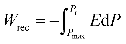
Fig. 1(a) shows the representative polarization–electric field (P–E) hysteresis loops of the capacitors with different dielectrics at 1 kHz after annealing at 450 °C for 30 min while keeping the total dielectric thickness at 10 nm. The capacitor with a single FE layer exhibits a square loop characteristic of the FE material. However, for the capacitor with a single AFE layer, pinched double hysteresis loops are clearly demonstrated, which should be ascribed to the electric field-induced AFE–FE phase transition.27 As the thickness of the incorporated FE layer increases from 1 to 5 nm, the fabricated capacitors still exhibit double hysteresis loops and the maximum polarization (Pmax) increases gradually from 22.2 to 27.4 μC cm−2 in contrast to 21.3 μC cm−2 for the single AFE layer. Fig. 1(b) shows the Weibull distribution of breakdown electric fields (EB) for the capacitors with different dielectrics. The mean value of EB can be extracted from the intersection of the fitting line and the X axis when Y = 0. Compared with the single AFE layer, the diverse FE/AFE stacks generate higher mean EB, i.e., 6.55–7.38 MV cm−1. Meanwhile, the resulting EB gradually increases with the increase of the FE thickness. This is because the dielectric constant of the AFE layer is greater than that of the FE layer.26 Based on the Gauss law and Kirchhoff voltage law, the introduction of the FE layer reduces the electric field across the AFE layer in the FE/AFE stack, and at the same time, the generated electric field across the AFE layer decreases gradually with the increase of the FE layer thickness at a fixed external bias.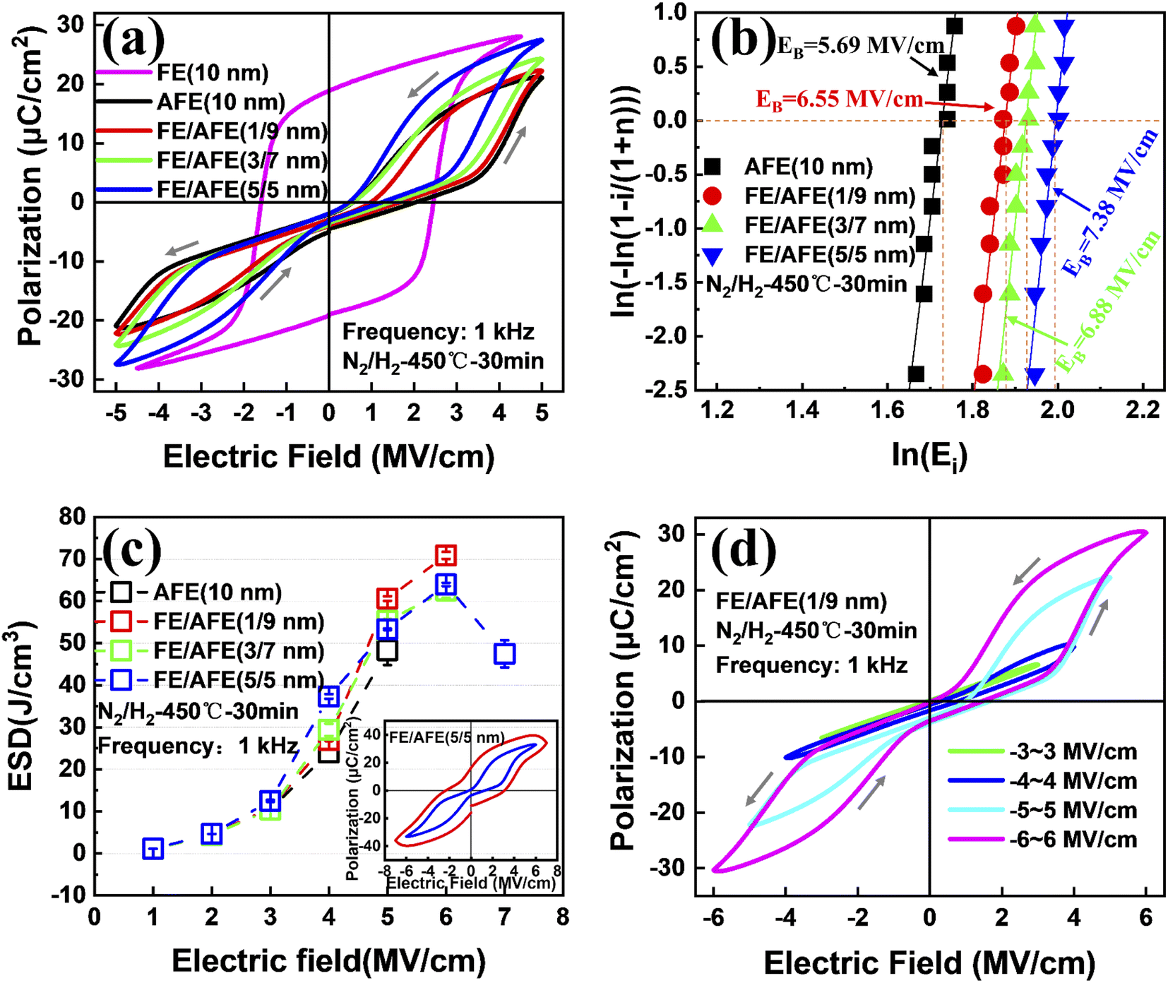 | ||
| Fig. 1 (a) Typical P–E hysteresis loops of the capacitors with different FE/AFE stacks as well as a single FE or AFE layer while keeping the total dielectric thickness at 10 nm; (b) Weibull distributions of breakdown electric fields for the capacitors with the FE/AFE stacks and the single AFE layer; (c) the ESD of the above capacitors as a function of an external electric field (10 devices were measured for each sample), the inset shows the P–E hysteresis loop of the capacitor with the FE/AFE (5/5 nm) stack at 6 MV cm−1 and 7 MV cm−1, respectively; (d) dependence of the P–E hysteresis loops on the external electric field for the capacitor with the FE(1 nm)/AFE(9 nm) stack. | ||
The recoverable ESD (Wrec) of a capacitor can be calculated by the integration of the electric field by polarization, described as eqn (1):28
 | (1) |
On the other hand, the ratio of the recoverable ESD to the total stored energy density is defined as the ESE (η) of a capacitor, which can be calculated by using eqn (2)28
 | (2) |
Fig. 2 shows the calculated ESE and the maximum ESD for the capacitors with different FE/AFE compositions after annealing at 450 °C for 30 min. As the FE thickness increases from 0 to 5 nm at a fixed total dielectric thickness of 10 nm, the ESE decreases from 61% to 53%, demonstrating relatively small variations. Moreover, the composition of FE (1 nm)/AFE (9 nm) shows the largest ESD of 71.93 J cm−3, accompanied by an ESE as large as 57.6%.
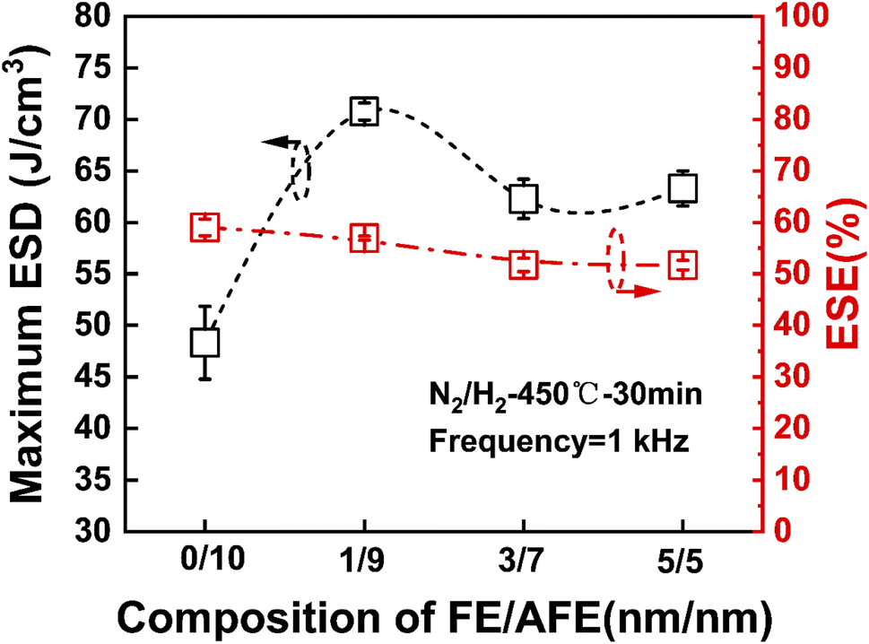 | ||
| Fig. 2 Comparison of the maximum ESD and the corresponding ESE for the capacitors with different FE/AFE compositions (ten devices are measured for each sample). | ||
To observe the effects of annealing temperature and annealing time on the ESD and ESE, the capacitors with the FE (1 nm)/AFE (9 nm) stack are further annealed under various annealing conditions. Fig. 3 shows the influences of annealing temperature and time on the maximum ESD and ESE for the FE (1 nm)/AFE (9 nm) capacitors. As the annealing temperature rises from 350 to 450 °C at a constant annealing time of 30 min, the obtained maximum ESD initially increases rapidly from 59.01 to 71.93 J cm−3, and then decreases to 67.47 J cm−3 at the annealing temperature of 500 °C. In addition, the corresponding ESE also demonstrates a similar variation trend, reaching a maximum value of 57.6% after annealing at 450 °C for 30 min. Further, the annealing time is also optimized at a fixed annealing temperature of 450 °C, as shown in Fig. 3(b). It is found that when the annealing time is maintained between 30 and 70 min, the resulting maximum ESD and ESE remain relatively stable, corresponding to 71.93 J cm−3 and ∼57.6%, respectively. However, both of them decrease for a shorter or longer annealing time (i.e., 10 or 90 min). When the annealing time is 10 min, it is possible that the FE/AFE stack is not fully crystallized and fails to form enough T-phase, resulting in lower ESD and ESE. When the annealing time increases to 90 min, the grain sizes of the FE/AFE layer become larger, resulting in a reduction in the relative content of the T-phase in the film because a larger grain size would be more favourable for the formation of the O-phase.29 Thus, the energy storage performance of the device deteriorates as the annealing time increases to 90 min. Therefore, 30 min annealing at 450 °C can be considered as the optimized annealing conditions for the capacitor with the FE (1 nm)/AFE (9 nm) stack.
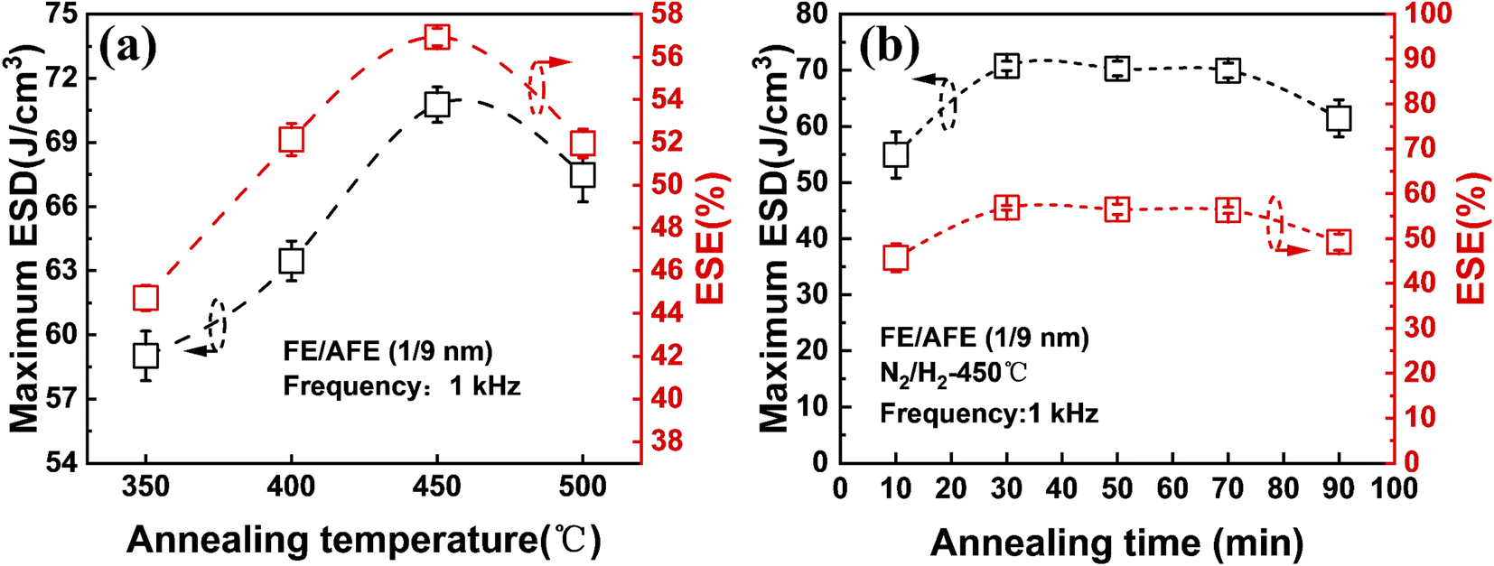 | ||
| Fig. 3 The maximum ESD and corresponding ESE of the capacitor with the FE (1 nm)/AFE (9 nm) stack: (a) at different annealing temperatures for 30 min; (b) at 450 °C for different annealing times. Ten devices are measured for each sample. | ||
To find out the influence of thermal annealing on the textures of the investigated dielectrics, the top TiN films of the TiN/dielectrics/TiN samples were removed by dry etching after post-annealing, and then the resulting samples were characterized by GIXRD, as shown in Fig. 4. As for the single AFE film and different FE/AFE stacks, an intense diffraction peak at ∼30° is observed after annealing at 450 °C for 30 min, which should be related to O- and T-phases, i.e., O (111)/T (101)/T (011) phases.22,30 Moreover, two weak diffraction peaks at ∼35.0° and ∼51.1° result from O (200)/T (110) and O (220)/T (200) phases, respectively, and the other two peaks originate from the TiN films.31,32 Since the 2θ values corresponding to the O (111) and T (101), (011) phases are very close for the Hf1−xZrxO2 films due to their structural similarities,31,33 the intense diffraction peak at ∼30° is further de-convoluted into several Gaussian peaks in order to clarify the phase composition, as shown in Fig. 4(b). Here, we only estimate the relative content of the T-/O- phase based on the most intense peak, and it does not represent the absolute content of the T-/O- phase in the film since another two weak diffraction peaks are also present at ∼35.0° and ∼51.1°, respectively. Regarding the single AFE layer, the resulting two peaks are located at 29.8° and 30.4°, corresponding to the T (011) and O (111) phases, respectively.31,33 For the FE/AFE stacks, the fitted two peaks appear at 29.8° and 30.17°, resulting from the T (011) and T (101) phases, respectively.33,34 The aforesaid results indicate that the introduction of a FE underlying film prevents the formation of the ferroelectric O (111)-phase and generates a new antiferroelectric T (101) phase. Such an increased proportion of the T-phase is beneficial to the AFE behavior.21 Further, as the FE layer increases from 1 to 5 nm, the relative percentage of the T (101) phase rises from 60% to 70%; however, the relative content of the T (011) phase decreases from 40% to 30%. Based on the intensity of the peak at ∼30°, it is found that the most T-phases are formed in the FE (1 nm)/AFE (9 nm) stack in comparison with the other stacks. This should correlate with a thicker AFE layer which is helpful to enhance the T-phase texture. In short, the incorporation of the underlying FE film even as thin as 1 nm affects the enhancement of the AFE phases. Fig. 4(c) shows the GIXRD patterns of the FE (1 nm)/AFE (9 nm) stack as a function of annealing temperature at a constant annealing time of 30 min. It can be observed that the diffraction peaks gradually enhance with the annealing temperature, especially when the annealing temperature reaches 450 °C or higher. This indicates that the grains formed in the FE/AFE stacks grow up gradually with the increase of annealing temperature. For example, according to the Scherrer formula, the calculated average grain sizes are equal to ∼6.1 nm and ∼7.8 nm, respectively, in terms of 450 and 500 °C annealing temperatures. A smaller grain size means the presence of more grain boundaries in the thin films, which is favorable for the formation of T-phases associated with the AFE behaviors.29,32 Further, the most intense diffraction peak associated with the O (111)/T (101)/T (011) phases is fitted with Gaussian functions, as shown in Fig. 4(d). In terms of 350 °C annealing, two components corresponding to the T (011) and O (111) phases are deduced. Owing to the existence of the ferroelectric O (111) phase, the resulting maximum ESD is rather low. When the annealing temperature increases to 400 °C, the O (111) phase disappears and the antiferroelectric T (101) phase comes into being. Therefore, the total content of the antiferroelectric T (011) and (101) phases increases in the sample, leading to a further increase in the ESD. After annealing at 450 °C for 30 min, the peaks associated with the T (011) and (101) phases become more intense, indicating a significant increase in the T phases. This should give rise to a rapid rise in the ESD. However, when the annealing temperature is elevated to 500 °C, one additional O (111) phase is formed, accounting for 17% of the total peak aera. This means that the T phase content is reduced, hence resulting in a decrease in the ESD. The above analyses are in good agreement with the change of ESD with annealing temperature, as shown in Fig. 3(a). In a word, our experimental results confirm that the composition of FE (1 nm)/AFE (9 nm) can achieve the optimal energy storage performance at the annealing temperature of 450 °C.
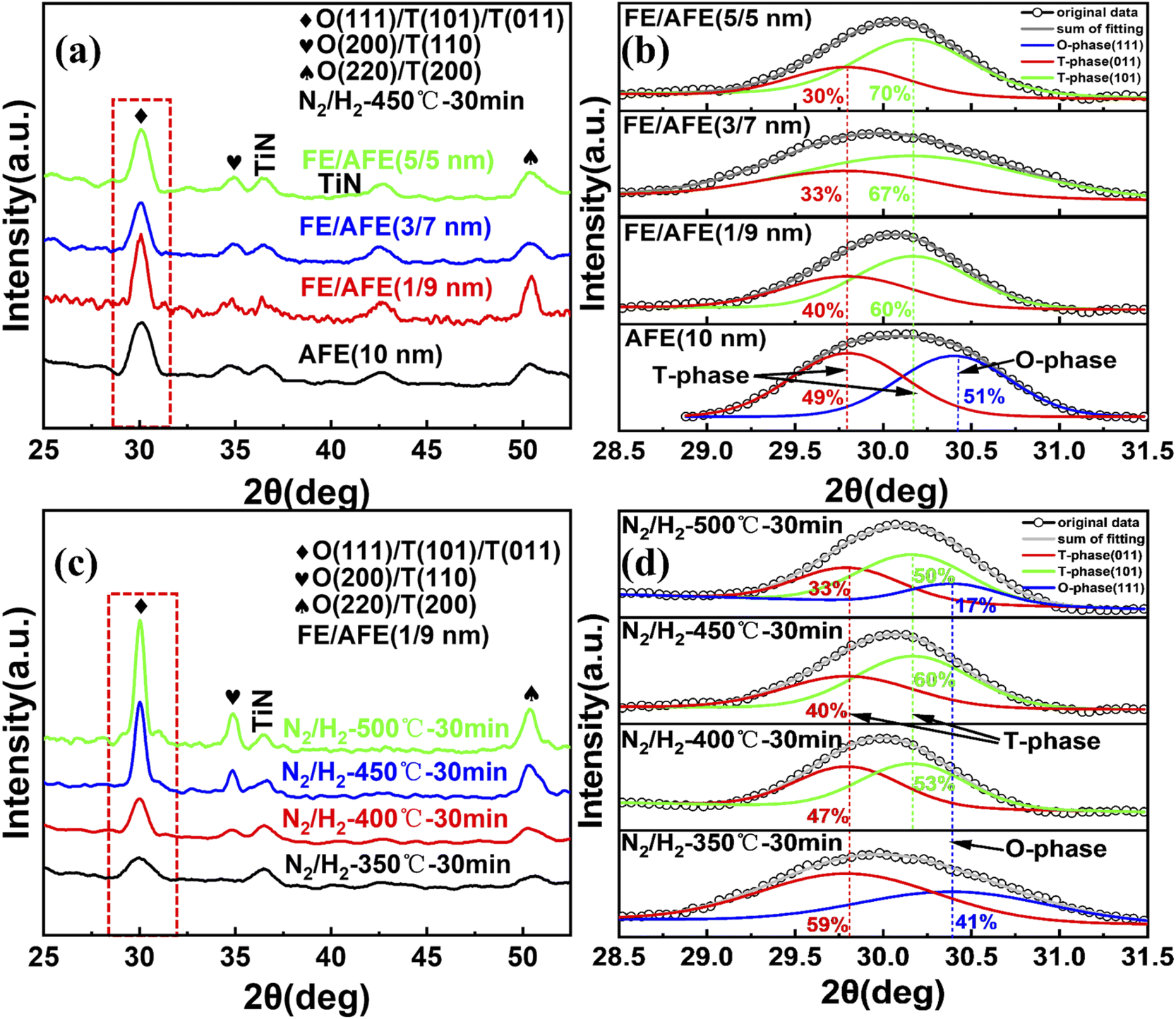 | ||
| Fig. 4 (a) GIXRD patterns and (b) de-convolution of the diffraction peak of O (111)/T (101)/T (011) for the single AFE film and different FE/AFE stacks on the TiN film after annealing at 450 °C for 30 min; (c) GIXRD patterns and (d) de-convolution of the peak of O (111)/T (101)/T (011) for the FE (1 nm)/AFE (9 nm) stack on the TiN film after annealing at different temperatures for 30 min. | ||
Fig. 5(a) and (b) show the cross-sectional TEM image and corresponding EDS maps of various elements for the TiN/FE (1 nm)/AFE (9 nm)/TiN capacitor, demonstrating a uniform dielectric thickness and clear interfaces of HfxZr1−xO2/TiN. In addition, the interface of FE (1 nm)/AFE (9 nm) cannot be distinguished intuitively, which is due to the similar elemental composition in the FE and AFE layers and the ultrathin thickness of FE. Further, the elemental profiles along the cross-section of the capacitor are drawn in Fig. 5(c). It is found that the atomic fractions of Hf and Zr display distinct variations near 60 nm, that is, the atomic ratio of Hf/Zr increases from 1:3 (i.e., 12.2%/35.6%) to 1:1 (i.e., 23.2%/24.3%). Meanwhile, the plateau width corresponding to Hf/Zr = 1:3 is much larger than that associated with Hf/Zr = 1:1. Thus, this discloses the transition from the Hf0.25Zr0.75O2 (AFE) layer to the Hf0.5Zr0.5O2 (FE) layer, which is in accord with our experimental design. For comparison, the elemental profiles of the single AFE (10 nm) capacitor are also demonstrated in Fig. 5(d). Both Zr and Hf profiles exhibit stable plateaus, in which the atomic ratio of Hf/Zr is kept at 1:3 (i.e., 12.6%/35.9%). This is also consistent with the composition of the AFE layer.
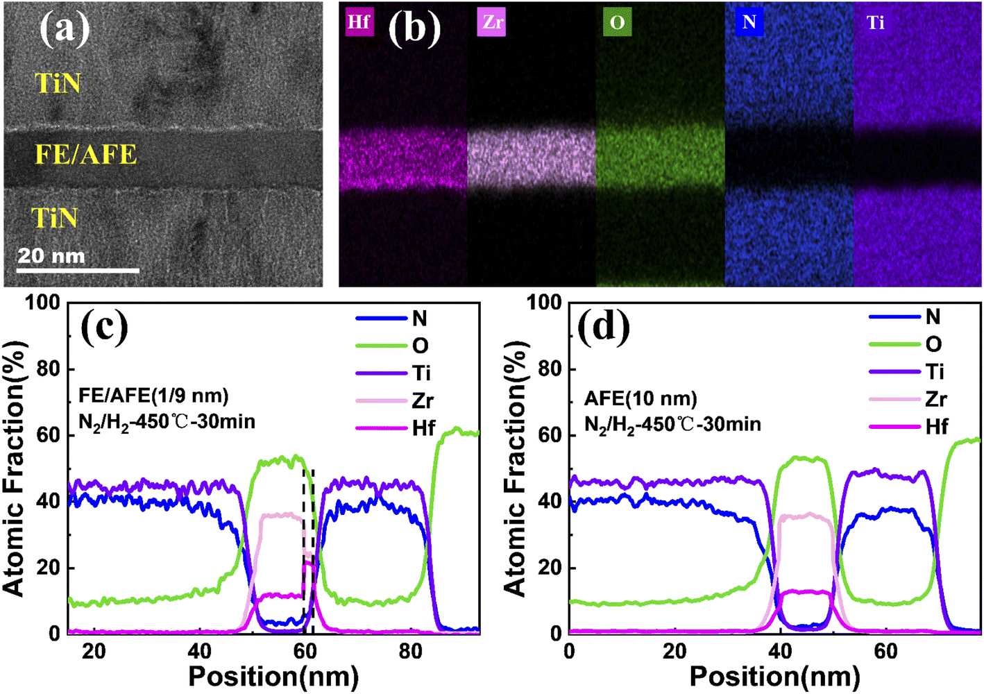 | ||
| Fig. 5 (a) Cross-sectional TEM image and (b) the corresponding EDS maps of Hf, Zr, O, N, and Ti elements for the FE (1 nm)/AFE (9 nm) capacitor; cross-sectional profiles of the elements from (c) the FE (1 nm)/AFE (9 nm) capacitor and (d) the single AFE (10 nm) capacitor, respectively. | ||
For insight into the effect of annealing temperature on the microstructures of the AFE and FE layers, HRTEM analyses are carried out on the FE (1 nm)/AFE (9 nm) sample annealed at different temperatures, as shown in Fig. 6. In terms of 400 °C annealing, crystalline T (101), (011), (200) phases and amorphous texture are coexistent in the AFE layer according to the FFT diffractograms of selected areas, as shown in Fig. 6(a). After annealing at 450 °C, the AFE layer becomes fully crystalline, revealing the coexistence of T (101), (011), and (200) phases, as indicated in Fig. 6(b). When the annealing temperature increases to 500 °C, the T (101), (011), and (200) phases still exist in the AFE layer, but the O (111) phase is also observed in some selected regions, see Fig. 6(c). This indicates that an excessively high annealing temperature can induce partial transformation of the T phase into the O phase, hence inhibiting the contributions from the AFE component. On the other hand, as for the single AFE capacitor annealed at 450 °C for 30 min, the O (111) phase is coexistent with the T (011) and (200) phases, as shown in Fig. 6(d). This causes a decrease in the proportion of the T-phase in the AFE film, so the AFE behavior and the ESD are weakened. To sum up, the above HRTEM analyses further confirm the XRD results in Fig. 4; meanwhile, the introduction of an ultrathin underlying FE layer changes the crystallization behaviors of the AFE film, and is beneficial to the formation of the AFE T-phases especially at the annealing temperature of 450 °C. Thus, the resulting energy storage performance is greatly improved compared with the single AFE capacitor.
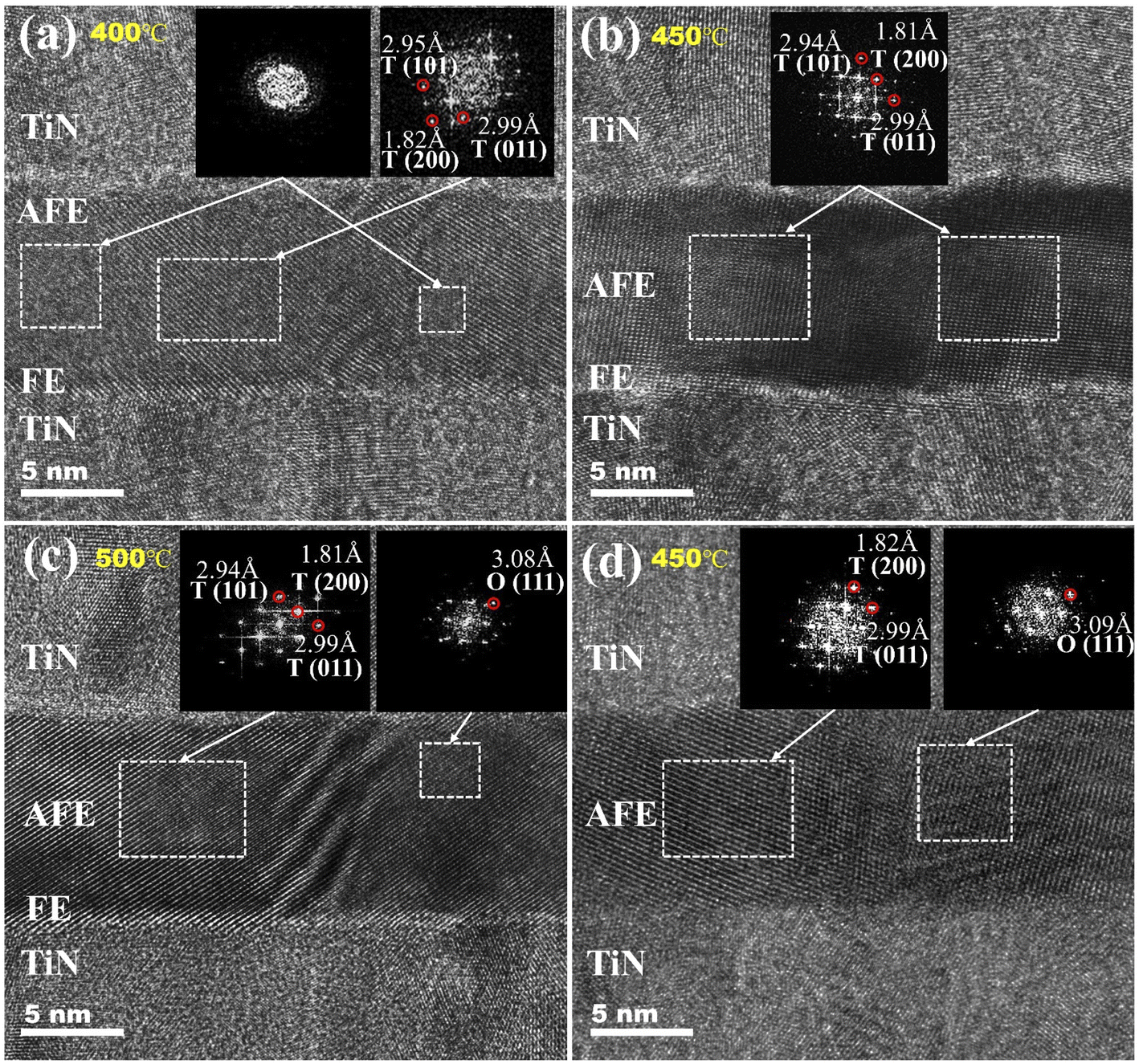 | ||
| Fig. 6 Cross-sectional HRTEM images and FFT (insets) of the FE (1 nm)/AFE (9 nm) stack annealed for 30 min at (a) 400 °C, (b) 450 °C and (c) 500 °C, respectively. (d) Cross-sectional HRTEM image and FFT (insets) of the single AFE layer annealed at 450 °C for 30 min. | ||
To further explore the effect of annealing temperature on the electrical cycling endurance of the FE (1 nm)/AFE (9 nm) capacitors, the P–E loops of the capacitors annealed at different temperatures are measured as a function of electrical pulse cycles, and the extracted energy storage performance is shown in Fig. 7(a). It is found that the capacitor annealed at 450 °C still exhibits the largest ESD and ESE after 106 operating cycles at 5 MV cm−1, and the corresponding degradation rates are close to 13.2% and 2.7%, respectively. However, both the capacitors annealed at 400 °C and 500 °C show larger degradation rates of ESD and ESE, which are equal to 16.4% and 4.6%, 23.7% and 15.6%, respectively. Furthermore, both the maximum ESD and the corresponding ESE are also extracted at different measurement temperatures for the capacitor annealed at 450 °C for 30 min, as illustrated in Fig. 7(b). It is observed that the maximum ESD and ESE demonstrate reductions of only 10% and 4%, respectively, with the increase of measurement temperature from 300 to 425 K. This also indicates that the FE (1 nm)/AFE (9 nm) capacitors have excellent temperature stability for energy storage applications.
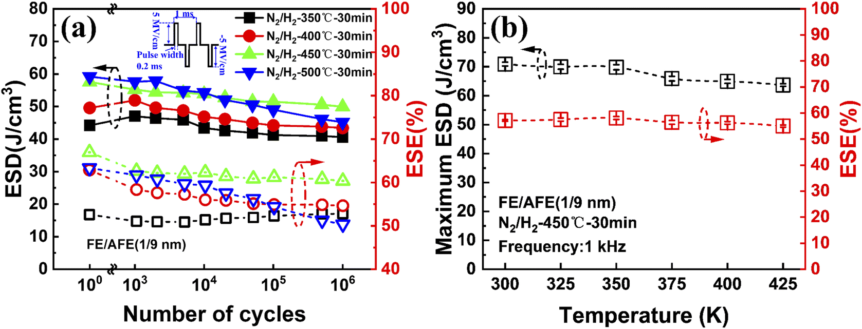 | ||
| Fig. 7 (a) Evolution of the ESD and ESE with the number of electrical pulse cycles (switching frequency: 1 kHz; pulse amplitude: ±5 MV cm; pulse width: 0.2 ms; waveform: square) for the FE (1 nm)/AFE (9 nm) capacitor annealed at different temperatures for 30 min, respectively; (b) dependence of the maximum ESD and corresponding ESE on measurement temperature for the FE (1 nm)/AFE (9 nm) capacitor annealed at 450 °C for 30 min (ten devices are measured at each temperature). | ||
It is well known that a much higher ESD per footprint unit can be realized through integration of the capacitor into a 3-D template because of a significant increase in the surface area of electrodes. Therefore, it is of significance to integrate the FE (1 nm)/AFE (9 nm) capacitor into deep silicon trenches. Fig. 8(a) shows the schematic of the fabricated 3-D capacitor, and the corresponding cross-sectional SEM image is shown in Fig. 8(b). Regular trenches with vertical and smooth side walls are obtained successfully, showing an aspect ratio of 7:1. Moreover, diverse material layers including TiN electrodes and HfxZr1−xO2 dielectrics are well filled into the trenches by PEALD (see the inset). The dependence of the P–E hysteresis loops on the external electric field for the 3-D trench capacitor with the FE (1 nm)/AFE (9 nm) stack is shown in Fig. 8(c), and as the maximum electric field increases from 1 to 5.7 MV cm−1, the resulting P–E loops gradually widen, and the max polarization per footprint unit increases from 13.3 to 163.2 μC cm−2. The green area indicates the recoverable ESD (Wrec), which can be calculated by the integration of the electric field by polarization per footprint unit. As shown in Fig. 8(d), compared with the planar capacitor, the polarization per footprint unit for the 3-D trench capacitor greatly increases, which is attributed to a significant increase in the actual electrode area of the 3-D capacitor since the total stored charges are proportional to the capacitor area. Fig. 8(e) shows the ESD and ESE of the fabricated 3-D capacitor under different electric fields. As the electric field increases from 1 to 5.7 MV cm−1, the ESD increases gradually from 6.45 to 358.14 J cm−3, however, the ESE decreases from 95% to 56%. In particular, when the electric field is larger than 3 MV cm−1, the ESE exhibits a remarkable decrease. This is because the enlarged P–E hysteresis loop leads to a larger hysteresis loss. To evaluate the uniformity of the fabricated 3-D capacitors, 30 devices are measured in comparison with the planar capacitors. The Weibull distributions of the extracted maximum ESD and ESE are shown in Fig. 8(f). It is found that the 3-D capacitors demonstrate a mean ESD of 364.1 J cm−3, which is around five times that (71.95 J cm−3) for the planar capacitors. In addition, although the planar capacitors display excellent electrical uniformity, the 3-D capacitors also have a quite narrow distribution of maximum ESD. On the other hand, both the planar and 3-D capacitors exhibit very close ESEs, corresponding to 57.8% and 56.5%, respectively.
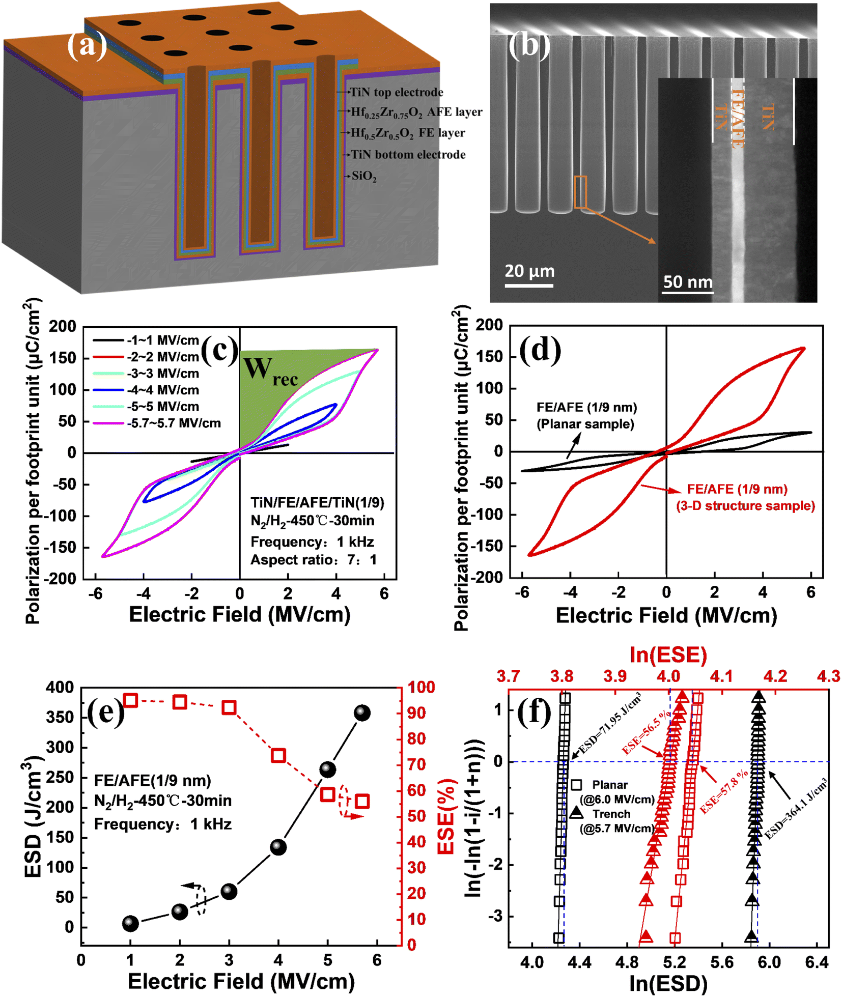 | ||
| Fig. 8 (a) Schematic of a 3-D trench capacitor; (b) cross-sectional SEM image of the 3-D capacitors with the FE (1 nm)/AFE (9 nm) stack, which are fabricated on the silicon trench substrate with an aspect ratio of 7:1; (c) dependence of the P–E hysteresis loops on the external electric field for the 3-D trench capacitor with the FE (1 nm)/AFE (9 nm) stack; (d) P–E hysteresis loops for a planar and a 3D FE (1 nm)/AFE (9 nm) stack-based capacitor; (e) the extracted ESD and ESE as a function of the electric field for the 3-D capacitor; (f) Weibull distributions of the extracted maximum ESD and ESE for the 3-D and planar capacitors (30 devices are measured for each kind of capacitor). | ||
Fig. 9 compares the ESDs and ESEs of our FE (1 nm)/AFE (9 nm) capacitors and the reported HfO2/ZrO2-based single AFE capacitors.35–37 It can be observed that our planar capacitor demonstrates the highest ESD compared with other HfO2/ZrO2-based single AFE capacitors, which should be attributed to the introduction of an ultrathin FE layer between the AFE layer and the TiN electrode, hence enhancing the formation of the AFE T-phases. Further, our 3-D capacitor shows much greater superiority in ESD than others while holding an above average ESE. By increasing the density and aspect ratio of trenches, the resulting ESD can be vastly elevated. Thus, the 3-D FE/AFE capacitors provide a promising opportunity for practical on-chip energy storage applications.
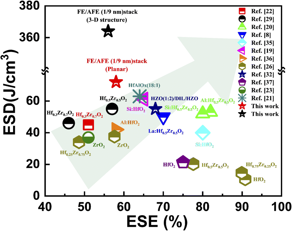 | ||
| Fig. 9 Comparison of the achievable ESD and the ESE between our FE/AFE stack capacitors and other HfO2/ZrO2-based single AFE capacitors. | ||
Conclusion
The FE-Hf0.5Zr0.5O2/AFE-Hf0.25Zr0.75O2 capacitors with TiN electrodes are fabricated using the PE-ALD technique. By optimizing the FE/AFE thickness composition and post-annealing conditions, the highest ESD planar capacitors are obtained for the 1 nm FE/9 nm AFE bilayer after annealing at 450 °C for 30 min, i.e., the resulting ESD and ESE are equal to 71.95 J cm−3 and 57.8% at 6 MV cm−1, respectively. This should be attributed to the introduction of the ultrathin FE layer between the AFE layer and the TiN electrode, hence enhancing the formation of the T phase with antiferroelectricity in the AFE Hf0.25Zr0.75O2 layer. Meanwhile, compared with the single AFE capacitor, the introduction of the 1 nm FE layer increases the breakdown electric field of the FE/AFE capacitor. Moreover, the FE (1 nm)/AFE (9 nm) bilayer capacitors also demonstrate superior electrical cycling endurance, and an excellent temperature stability from 300 to 425 K, which makes them more competitive for applications in high-temperature environments. Further, by integrating the capacitor into deep silicon trenches, a superhigh ESD of 364.1 J cm−3 is achieved together with an ESE of 56.5%. The current study provides a new strategy to achieve CMOS process-compatible, eco-friendly and superhigh ESD capacitors for practical on-chip energy storage applications.Author contributions
The manuscript was written through contributions of all authors. All authors have given approval to the final version of the manuscript.Conflicts of interest
There are no conflicts to declare.Acknowledgements
This work was supported in part by the National Natural Science Foundation of China under Grant 61874029.References
- C. Lethien, J. Le Bideau and T. Brousse, Energy Environ. Sci., 2019, 12, 96–115 RSC.
- J. Liu, J. Supercomput., 2021, 1–18 Search PubMed.
- N. Qi, Y. Yin, K. Dai, C. Wu and Z. You, Appl. Energy, 2021, 290, 116780 CrossRef.
- E. Chemali, M. Preindl, P. Malysz and A. Emadi, IEEE Trans. Emerg. Sel. Topics Power Electron., 2016, 4, 1117–1134 Search PubMed.
- L. C. Haspert, S. B. Lee and G. W. Rubloff, ACS Nano, 2012, 6, 3528 CrossRef CAS PubMed.
- J. Rui, B. Gs, C. Fq and C. A. Di, Energy Storage Mater., 2020, 27, 169–186 CrossRef.
- I. Lucia, V. Victor, G. A. Javier, H. Blanca and V. M. Prida, Front. Phys., 2015, 3, 1 Search PubMed.
- M. G. Kozodaev, A. G. Chernikova, R. R. Khakimov, M. H. Park, A. M. Markeev and C. S. Hwang, Appl. Phys. Lett., 2018, 113, 123902 CrossRef.
- Z. Liu, T. Lu, J. Ye, G. Wang, X. Dong, R. Withers and Y. Liu, Adv. Mater. Technol., 2018, 3, 1800111 CrossRef.
- A. Hp, B. Mp, B. Au, C. Jpbs, B. Gth and D. Jr, Ferroelectric Materials for Energy Harvesting and Storage, 2021, pp. 279–356 Search PubMed.
- L.-J. Li, B. Zhu, S.-J. Ding, H.-L. Lu, Q.-Q. Sun, A. Jiang, D. W. Zhang and C. Zhu, Nanoscale Res. Lett., 2012, 7, 1–5 CrossRef PubMed.
- H. Palneedi, M. Peddigari, G. T. Hwang, D. Y. Jeong and J. Ryu, Adv. Funct. Mater., 2018, 28, 1803665 CrossRef.
- Q. Li, F.-Z. Yao, Y. Liu, G. Zhang, H. Wang and Q. Wang, Annu. Rev. Mater. Res., 2018, 48, 219–243 CrossRef CAS.
- Y. Guo, M. Gu, H. Luo, Y. Liu and R. L. Withers, Phys. Rev. B: Condens. Matter Mater. Phys., 2011, 83, 054118 CrossRef.
- I. V. Ciuchi, L. Mitoseriu and C. Galassi, J. Am. Ceram. Soc., 2016, 99, 2382–2387 CrossRef CAS.
- D. Fu, M. Endo, H. Taniguchi, T. Taniyama and M. Itoh, Appl. Phys. Lett., 2007, 90, 252907 CrossRef.
- M. Zhang, S. Tan, J. Xiong, C. Chen, Y. Zhang, X. Wei and Z. Zhang, ACS Appl. Energy Mater., 2021, 4, 8454–8464 CrossRef CAS.
- H. Cheng, J. Ouyang, Y.-X. Zhang, D. Ascienzo, Y. Li, Y.-Y. Zhao and Y. Ren, Nat. Commun., 2017, 8, 1–7 CrossRef PubMed.
- F. Ali, X. Liu, D. Zhou, X. Yang, J. Xu, T. Schenk, J. Müller, U. Schroeder, F. Cao and X. Dong, J. Appl. Phys., 2017, 122, 144105 CrossRef.
- P. D. Lomenzo, C. C. Chung, C. Zhou, J. L. Jones and T. Nishida, Appl. Phys. Lett., 2017, 110, 232904 CrossRef.
- J. Zhou, Y. Kang, X. Wang, Z. Zhou, H. Ni, L. Jiao, Z. Zheng and X. Gong, J. Phys. D: Appl. Phys., 2021, 55, 014003 CrossRef.
- M. H. Park, H. J. Kim, Y. J. Kim, T. Moon, K. D. Kim and C. S. Hwang, Adv. Theory Simul., 2014, 4, 1400610 Search PubMed.
- M. Pešić, M. Hoffmann, C. Richter, T. Mikolajick and U. Schroeder, Adv. Funct. Mater., 2016, 26, 7486–7494 CrossRef.
- T. Zhang, W. Li, Y. Zhao, Y. Yu and W. Fei, Adv. Funct. Mater., 2018, 28, 1706211 CrossRef.
- T. Zhang, W. Li, Y. Hou, Y. Yu, R. Song, W. Cao and W. Fei, J. Am. Ceram. Soc., 2017, 100(7), 3080–3087 CrossRef CAS.
- S. J. Kim, J. Mohan, J. S. Lee, H. S. Kim, J. Lee, C. D. Young, L. Colombo, S. R. Summerfelt, T. San and J. Kim, ACS Appl. Mater. Interfaces, 2019, 11, 5208–5214 CrossRef CAS PubMed.
- K. Chae, J. Hwang, E. Chagarov, A. Kummel and K. Cho, J. Appl. Phys., 2020, 128, 054101 CrossRef CAS.
- A. Chauhan, S. Patel, R. Vaish and C. R. Bowen, Materials, 2015, 8, 8009–8031 CrossRef PubMed.
- K. D. Kim, Y. H. Lee, T. Gwon, Y. J. Kim, H. J. Kim, T. Moon, S. D. Hyun, H. W. Park, M. H. Park and C. S. Hwang, Nano Energy, 2017, 39, 390–399 CrossRef CAS.
- A. Kashir, M. G. Farahani and H. Hwang, Nanoscale, 2021, 13, 13631–13640 RSC.
- D.-Q. Xiao, B.-B. Luo, W. Xiong, X. Wu, D. W. Zhang and S.-J. Ding, IEEE Trans. Electron Devices, 2021, 68, 6359–6364 CAS.
- D. Das, V. Gaddam and S. Jeon, IEEE Electron Device Lett., 2021, 42, 331–334 CAS.
- J. Muller, T. S. Boscke, U. Schroder, S. Mueller, D. Brauhaus, U. Bottger, L. Frey and T. Mikolajick, Nano Lett., 2012, 12, 4318–4323 CrossRef PubMed.
- S. S. Cheema, N. Shanker, L.-C. Wang, C.-H. Hsu, S.-L. Hsu, Y.-H. Liao, M. San Jose, J. Gomez, W. Chakraborty and W. Li, Nature, 2022, 604, 65–71 CrossRef CAS PubMed.
- M. Hoffmann, U. Schroeder, C. Künneth, A. Kersch, S. Starschich, U. Böttger and T. Mikolajick, Nano Energy, 2015, 18, 154–164 CrossRef CAS.
- M. H. Park, T. Schenk, M. Hoffmann, S. Knebel, J. Gärtner, T. Mikolajick and U. Schroeder, Nano Energy, 2017, 36, 381–389 CrossRef CAS.
- L. Zhang, M. Liu, W. Ren, Z. Zhou, G. Dong, Y. Zhang, B. Peng, X. Hao, C. Wang and Z.-D. Jiang, RSC Adv., 2017, 7, 8388–8393 RSC.
| This journal is © The Royal Society of Chemistry 2022 |