
Green organic light-emitting devices with external quantum efficiency up to nearly 30% based on an iridium complex with a tetraphenylimidodiphosphinate ligand
Yanan Lia,
Liang Zhou*a,
Yunlong Jianga,
Rongzhen Cuia,
Xuesen Zhaoa,
Youxuan Zheng*b,
Jinglin Zuob and
Hongjie Zhang*a
aState Key Laboratory of Rare Earth Resource Utilization, Changchun Institute of Applied Chemistry, Chinese Academy of Sciences, Changchun 130022, People's Republic of China. E-mail: zhoul@ciac.ac.cn; hongjie@ciac.ac.cn; Fax: +86 43185685653; Tel: +86 43185262127
bState Key Laboratory of Coordination Chemistry, Collaborative Innovation Center of Advanced Microstructures, School of Chemistry and Chemical Engineering, Nanjing University, Nanjing 210023, People's Republic of China. E-mail: yxzheng@nju.edu.cn
First published on 28th June 2016
Abstract
In this work, a series of electroluminescent (EL) devices with single- or double-light-emitting layer(s) (EML) were fabricated to further improve the EL performances of green iridium complex (tfmppy)2Ir(tpip) (tfmppy = 4-trifluoromethylphenylpyridine, tpip = tetraphenylimido-diphosphinate). p-Type material 4,4′,4′′-tri-s(carbazole-9-yl)triphenylamine and bipolar material 2,6-bis(3-(9H-carbazol-9-yl)phenyl)pyridine were chosen as host materials of EML1 and EML2, respectively. Experimental results displayed that not only the doping concentration but also the thicknesses of EML and the electron transport layer strongly influence device performances. Finally, a high performance green EL device with maximum brightness, current efficiency, power efficiency and external quantum efficiency (EQE) up to 113![[thin space (1/6-em)]](https://www.rsc.org/images/entities/char_2009.gif) 610 cd m−2, 112.30 cd A−1, 97.95 lm W−1 and 29.4%, was realized. Even at the practical brightness of 1000 cd m−2, current efficiency as high as 107.6 cd A−1 (EQE = 28.1%) can still be retained by the same device. To our best knowledge, EL performances of this device were amongst the highest results of the previously reported green devices.
610 cd m−2, 112.30 cd A−1, 97.95 lm W−1 and 29.4%, was realized. Even at the practical brightness of 1000 cd m−2, current efficiency as high as 107.6 cd A−1 (EQE = 28.1%) can still be retained by the same device. To our best knowledge, EL performances of this device were amongst the highest results of the previously reported green devices.
1. Introduction
Organic light-emitting devices (OLEDs) have attracted great interest throughout the world owing to their potential application in solid-state lighting and in full-color flat panel displays.1–4 Phosphorescent transition metal complexes have been increasingly used in OLEDs because phosphors can harvest both singlet and triplet excitons thus realizing the theoretical 100% internal quantum efficiency.5–8 Amongst these complexes, trivalent iridium (Ir(III)) complexes have been intensively studied because of their high phosphorescent efficiencies and relatively short excited state lifetimes.9–11 In the past years, many groups have given their attention to the design of Ir(III) complexes and the optimization of device structures.12–14 Significant enhancement of maximum electroluminescent (EL) efficiencies has been achieved, but EL efficiencies of most reported devices drop rapidly with increasing current density due to triplet–triplet annihilation, triplet-polaron annihilation, and electric field induced dissociation of excitons.15 Such inherent roll-off of EL efficiency is quite severe in phosphorescent OLEDs and detrimentally degrades the device working performances for practical applications particularly at high luminance.In 2011, we reported the synthesis and EL performances of the green emitter (tfmppy)2Ir(tpip) (tfmppy = 4-trifluoromethylphenylpyridine, tpip = tetraphenylimido-diphosphinate), which possesses high electron mobility and short excited state lifetime.12 By doping (tfmppy)2Ir(tpip) into the bipolar host material 1,3-bis(carbazol-9-yl)benzene (mCP), green EL device with the maximum current efficiency of 67.95 cd A−1 and power efficiency of 69.90 lm W−1 was obtained. Moreover, the roll-off of EL efficiency in these devices was significantly suppressed due to the broadening of the recombination zone. However, hole mobility of mCP is relatively higher than its electron mobility, which causes the unbalanced distribution of holes and electrons on emitter molecules within the light-emitting layer (EML), thus limiting the improvement of EL efficiency. Later, device structure was further optimized by doping (tfmppy)2Ir(tpip) into hole block material 2,2′,2′′-(1,3,5-benzinetriyl)-tris(1-phenyl-1-H-benzimidazole) (TPBi) as the supplementary EML, which was demonstrated to be helpful in balancing carriers' distribution, broadening the recombination zone and even facilitating the trapping of carriers.16 Although certain improvement have been realized, EL performances of devices based on (tfmppy)2Ir(tpip) are still not satisfactory compared with the theoretical values. Therefore, more efforts should be paid on the optimization of device structures to further improve the EL performances of (tfmppy)2Ir(tpip).
In this work, we aim to further improve the EL performances of (tfmppy)2Ir(tpip) by designing the double-EMLs device structure, which has been demonstrated to be efficient in improving EL efficiency, confining recombination zone as well as delaying the roll-off of EL efficiency.17,18 A series of devices with single- or double-EML(s) were fabricated and compared by doping (tfmppy)2Ir(tpip) into two different materials with stepwise energy levels. Finally, high performance green EL device with maximum brightness, current efficiency, power efficiency and external quantum efficiency (EQE) up to 113610 cd m−2, 112.30 cd A−1, 97.95 lm W−1 and 29.4%, respectively, was realized by optimizing the doping concentration, the thicknesses of EML and electron transport layer. Even at the practical brightness of 1000 cd m−2, current efficiency as high as 107.6 cd A−1 (EQE = 28.1%) can still be retained.
2. Experiment
All the organic materials used in this study were obtained commercially and used as received without further purification except for (tfmppy)2Ir(tpip), which was synthesized and purified in our laboratory. Indium-tin-oxide (ITO) coated glass with a sheet resistance of 10 Ω sq.−1 was used as the anode substrate. Prior to film deposition, patterned ITO substrates were cleaned with detergent, rinsed in de-ionized water, and dried in an oven. All organic layers were deposited with the rate of 0.1 nm s−1 under high vacuum (≤2.0 × 10⁻⁵ Pa). The EMLs were prepared by co-evaporating (tfmppy)2Ir(tpip) and host material from two individual sources, and the doping concentration was modulated by controlling the evaporation rate of (tfmppy)2Ir(tpip). MoO3, LiF and Al were deposited in another vacuum chamber (≤8.0 × 10⁻⁵ Pa) with the rates of 0.01, 0.01, and 1.0 nm s−1, respectively, without being exposed to the atmosphere. Current density–brightness–voltage (J–B–V) characteristics were measured by using a programmable Keithley source measurement unit (Keithley 2400 and Keithley 2000) with a silicon photodiode. The EL spectra were measured with a calibrated Hitachi F-7000 fluorescence spectrophotometer. The EQE of EL device was calculated based on the photo energy measured by the photodiode, the EL spectrum, and the current pass through the device.3. Results and discussion
Device structure and energy level diagram of the designed OLEDs are depicted in Fig. 1. In this work, (tfmppy)2Ir(tpip) was chosen as emitter due to its pure green emission and matched energy levels. MoO3 film was deposited upon indium-tin-oxide (ITO) layer as anode modification layer to improve the injection of holes. Di-[4-(N,N-ditolyl-amino)-phenyl]cyclohexane (TAPC), which possesses high hole mobility (1 × 10⁻² cm2 V−1 s−1) and high-lying LUMO level (−1.8 eV), was used as hole transport/electron block layer (HTL/EBL).19 1,3,5-Tri(m-pyrid-3-yl-phenyl)benzene (TmPyPB), which possesses low-lying HOMO level (−6.7 eV) and high electron mobility (1 × 10⁻³ cm2 V−1 s−1), was used as hole block/electron transport layer (HBL/ETL).20 The widely utilized p-type material 4,4′,4′′-tri-s(carbazole-9-yl)triphenylamine (TcTa) and bipolar material 2,6-bis(3-(9H-carbazol-9-yl)phenyl)pyridine (26DCzPPy) were chosen as host materials of EML1 and EML2, respectively.21 The molecular structures of (tfmppy)2Ir(tpip), TcTa and 26DCzPPy are also shown in Fig. 1.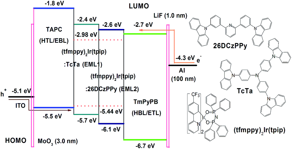 | ||
| Fig. 1 Proposed energy level diagram of the devices used in this work and the molecular structures of (tfmppy)2Ir(tpip), TcTa and 26DCzPPy. | ||
As been experimentally demonstrated in our previous reports, the stepwise HOMO levels of TAPC (−5.5 eV), TcTa (−5.7 eV), and 26DCzPPy (−6.1 eV) are beneficial for the injection and transport of holes,19,21,22 while the stepwise LUMO levels of TmPyPB (−2.7 eV), 26DCzPPy (−2.6 eV), and TcTa (−2.4 eV) are beneficial for the injection and transport of electrons.20–22 That means balanced distribution of carriers (holes and electrons) and wide recombination zone could be expected. More importantly, the LUMO level of TAPC is 0.6 eV higher than that of TcTa while the HOMO level of TmPyPB is 0.6 eV lower than that of 26DCzPPy; thus, holes and electrons are well confined within EMLs. Since the HOMO and LUMO levels of (tfmppy)2Ir(tpip) (−5.44 and −2.98 eV, respectively) are within those of TcTa and 26DCzPPy,12,21 carrier trapping is conceived to be the dominant EL mechanism of these devices.23,24
To optimize the doping concentration of (tfmppy)2Ir(tpip), three single-EML devices with the structure of ITO/MoO3 (3 nm)/TAPC (50 nm)/(tfmppy)2Ir(tpip) (x wt%):26DCzPPy (15 nm)/TmPyPB (50 nm)/LiF (1 nm)/Al (100 nm) and three double-EMLs devices with the structure of ITO/MoO3 (3 nm)/TAPC (50 nm)/(tfmppy)2Ir(tpip) (x wt%):TcTa (5 nm)/(tfmppy)2Ir(tpip) (x wt%):26DCzPPy (15 nm)/TmPyPB (50 nm)/LiF (1 nm)/Al (120 nm) were fabricated and examined by adjusting x to be 5, 6 and 7, respectively. Fig. 2 depicted the doping concentration dependence of EL efficiency–brightness characteristics. Current density–brightness–voltage characteristics of these devices were depicted in the insert of Fig. 2. The key performances of these six devices are summarized in Table 1. Experimental results displayed that 6 wt% is the optimal concentration of (tfmppy)2Ir(tpip) for both single- and double-EML(s) devices. As listed in Table 1, the 6 wt% doped double-EMLs device achieved the highest brightness of 94151 cd m−2, while the 6 wt% doped single-EML device obtained the highest EL efficiency and external quantum efficiency (EQE) of 106.33 cd A−1 and 26.2%, respectively. At the high brightness of 1000 cd m−2, EL efficiency and EQE as high as 103.08 cd A−1 and 25.4% can be retained by the 6 wt% doped single-EML device. But as shown in Fig. 2, compared with single-EML device, double-EMLs device displayed relatively slower roll-off of EL efficiency attributed to the broadening recombination zone. For example, at the high brightness of 10000 cd m−2, 6 wt% doped single-EML device retained the current efficiency of 81.59 cd A−1, while 6 wt% doped double-EMLs device retained the current efficiency of 88.30 cd A−1. Interestingly, devices with doping concentration of 7 wt% displayed lowest turn-on voltages. This phenomenon can be interpreted as the excellent electron transport ability of (tfmppy)2Ir(tpip), which causes the narrower recombination zone at relatively high doping concentration, thus the lower turn-on voltage and the faster efficiency roll-off. Fig. 3(a) given EL spectra of these devices operating at the current density of 10 mA cm−2. Apart from the characteristic emission of (tfmppy)2Ir(tpip) (peaked at about 527 nm), these devices displayed weak emission range from 380 to 430 nm, which originate from TcTa and 26DCzPPy. In this case, the emergence of weak TcTa and 26DCzPPy emissions in EL spectra can be attributed to the accumulation of holes and electrons within EMLs, which result in the transfer of few carriers from emitter onto host molecules. Consequently, few holes and electrons recombine on TcTa and 26DCzPPy molecules.
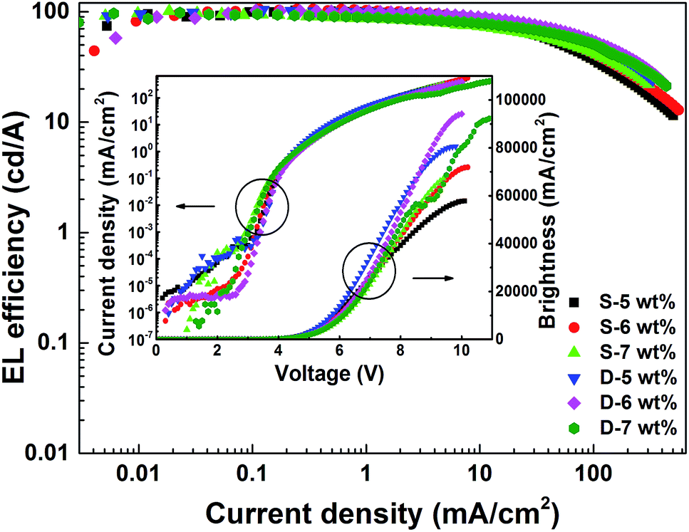 | ||
| Fig. 2 EL efficiency–brightness (η–B) characteristics of the single- and double-EML(s) devices with (tfmppy)2Ir(tpip) at different doping concentrations. Insert: current density–brightness–voltage (J–B–V) characteristics of the single- and double-EML(s) devices with (tfmppy)2Ir(tpip) at different doping concentrations. | ||
| Device | Vturn-on (V) | Ba (cd m−2) | ηcb (EQE c) (cd A−1) | ηpd (lm W−1) | ηce (cd A−1) (EQEf) (1000 cd m−2) | CIEx,yg |
|---|---|---|---|---|---|---|
| a The data for maximum brightness (B).b Maximum current efficiency (ηc).c Maximum external quantum efficiency (EQE).d Maximum power efficiency (ηp).e Current efficiency (ηc) at the certain brightness of 1000 cd m−2.f External quantum efficiency (EQE) at the certain brightness of 1000 cd m−2.g Commission Internationale de l'Eclairage coordinates (CIEx,y) at 10 mA cm−2. | ||||||
| S-5 wt% | 3.5 | 57852 |
102.41 (25.7%) | 83.11 | 100.00 (25.1%, 4.6 V) | (0.300, 0.655) |
| S-6 wt% | 3.4 | 71922 |
106.33 (26.2%) | 85.61 | 103.08 (25.4%, 4.6 V) | (0.297, 0.657) |
| S-7 wt% | 3.1 | 67291 |
101.53 (25.4%) | 93.77 | 86.49 (21.6%, 4.7 V) | (0.291, 0.663) |
| D-5 wt% | 3.6 | 80534 |
104.09 (25.8%) | 81.71 | 99.54 (24.6%, 4.6 V) | (0.299, 0.662) |
| D-6 wt% | 3.6 | 94151 |
103.10 (25.6%) | 80.93 | 100.96 (25.1%, 4.7 V) | (0.299, 0.661) |
| D-7 wt% | 3.2 | 92441 |
98.20 (25.3%) | 88.10 | 88.49 (22.8%, 4.7 V) | (0.291, 0.667) |
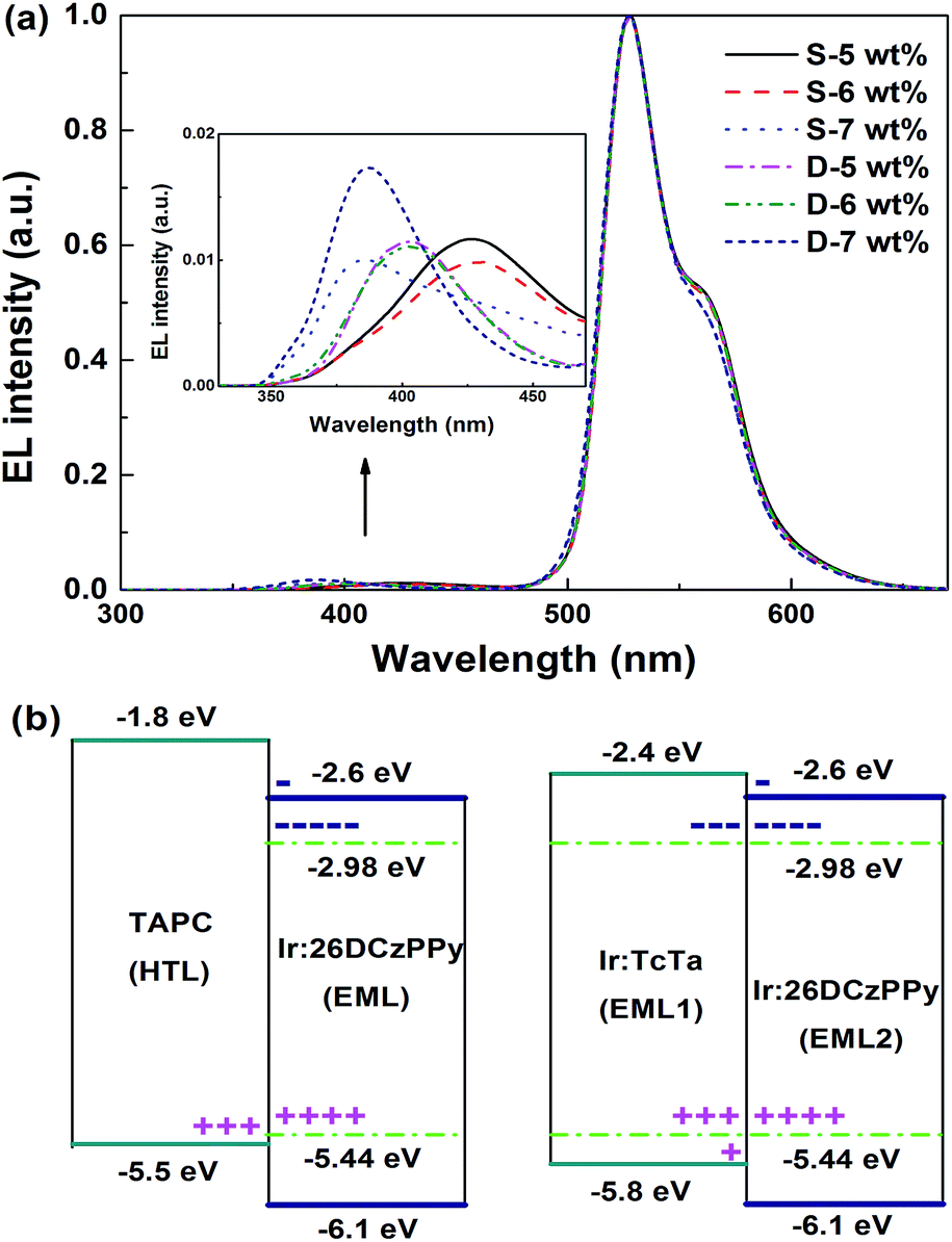 | ||
| Fig. 3 (a) Normalized EL spectra of the single- and double-EML(s) devices operating at the current density of 10 mA cm−2. (b) Schematic representation of carriers' distribution within the EML(s) of single-EML device (left) and double-EMLs device (right). Symbols − and + represent electrons and holes, respectively. | ||
To further improve the EL performances of (tfmppy)2Ir(tpip), as shown in Fig. 3(b), EL mechanisms of these single- and double-EML(s) devices were investigated by analyzing the distribution of holes and electrons within EML(s). For single-EML devices, holes and electrons accumulate in HTL and EML, respectively, near the interface of HTL/EML. For double-EMLs devices, holes and electrons accumulate in EML1 and EML2, respectively, near the interface of EML1/EML2. Compared with single-EML devices, double-EMLs devices possess improved hole injection ability from HTL into EMLs because the HOMO level of TcTa situates between those of TAPC and 26DCzPPy, thus causing the low hole injection barrier.25 Consequently, double-EMLs devices obtained better balance of carriers within EMLs, wider recombination zone and lower densities of triplet excitons within EMLs, thus realizing slower roll-off of efficiencies and higher brightness.
Based on the 6 wt% doped double-EML device, more devices were fabricated by further optimizing the thickness of EMLs. Experimental results revealed the thickness of EML1 has no differentiable influence on the EL performances attributed to the unipolar characteristic of TcTa. As shown in Fig. 4 and Table 2, keeping the thickness of EML1 constant, brightness and efficiencies increased firstly to a maximum value and then decreased gradually with increasing thickness of EML2. The device with 11 nm EML2 achieved the maximum brightness, EL efficiency, power efficiency and EQE of 111817 cd m−2, 106.53 cd A−1, 91.91 lm W−1 and 26.5%, respectively. At the certain brightness of 1000 cd m−2, current efficiency and EQE as high as 102.01 cd A−1 and 25.3% were retained by the same device. Fig. 5(a) given EL spectra of these devices operating at the current density of 10 mA cm−2. Besides the characteristic emission of (tfmppy)2Ir(tpip) (527 nm), weak emission of 26DCzPPy peaked at about 400 nm was also observed in these devices. Amongst these devices, the 11 nm device displayed the weakest 26DCzPPy emission with the Commission Internationale de l'Eclairage (CIE) coordinates of (0.298, 0.666). To examine the mechanism for the improved performance data of these devices, as shown in Fig. 5(b), the distribution of holes and electrons within EML(s) were also analyzed. With increasing thickness of EML2, the increasing electron transport distance causes the broadening recombination zone and the decreasing electron density within both EMLs. As a result, the distribution of holes and electrons tends toward balance firstly and then deteriorates gradually when the thickness of EML2 is thicker than 11 nm.
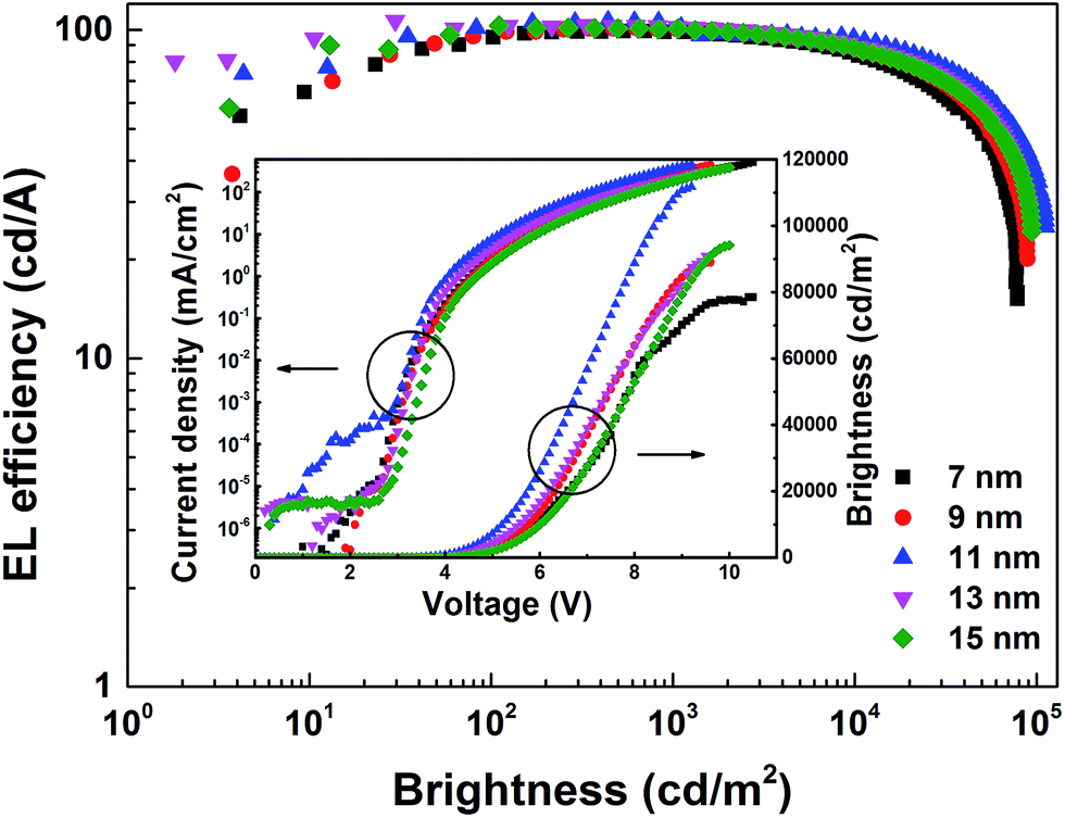 | ||
| Fig. 4 EL efficiency–brightness (η–B) characteriwstics of the devices with different thicknesses of EML2. Insert: current density–brightness–voltage (J–B–V) characteristics of the devices with different thicknesses of EML2. | ||
| Device | Vturn-on (V) | Ba (cd m−2) | ηcb (EQE c) (cd A−1) | ηpd (lm W−1) | ηce (cd A−1) (EQEf) (1000 cd m−2) | CIEx,yg |
|---|---|---|---|---|---|---|
| a The data for maximum brightness (B).b Maximum current efficiency (ηc).c Maximum external quantum efficiency (EQE).d Maximum power efficiency (ηp).e Current efficiency (ηc) at the certain brightness of 1000 cd m−2.f External quantum efficiency (EQE) at the certain brightness of 1000 cd m−2.g Commission Internationale de l'Eclairage coordinates (CIEx,y) at 10 mA cm−2. | ||||||
| 7 nm | 3.3 | 78562 |
99.30 (25.5%) | 78.67 | 98.64 (25.3%, 4.6 V) | (0.299, 0.663) |
| 9 nm | 3.4 | 89007 |
101.39 (26.3%) | 79.63 | 100.64 (26.1%, 4.6 V) | (0.296, 0.665) |
| 11 nm | 3.2 | 111817 |
106.53 (26.5%) | 91.91 | 102.01 (25.3%, 4.1 V) | (0.298, 0.666) |
| 13 nm | 3.2 | 90893 |
106.55 (26.5%) | 95.59 | 102.08 (25.4%, 4.3 V) | (0.298, 0.663) |
| 15 nm | 3.6 | 94151 |
103.10 (25.6%) | 80.93 | 100.96 (25.1%, 4.7 V) | (0.299, 0.661) |
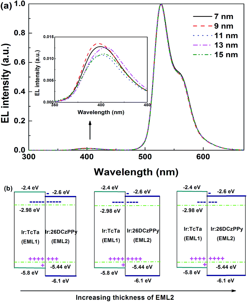 | ||
| Fig. 5 (a) Normalized EL spectra of the devices with different thicknesses of EML2 operating at the current density of 10 mA cm−2. (b) Schematic representation of carriers' distribution within the EMLs of the devices with different thicknesses of EML2. Symbols − and + represent electrons and holes, respectively. | ||
Subsequently, based on the device with 11 nm EML2, two other devices were designed and fabricated by decreasing the thickness of ETL from 50 nm to be 40 and 45 nm, respectively. Fig. 6(a) depicted the dependence of EL efficiency–brightness characteristics on the thickness of ETL. Current density–brightness–voltage characteristics of these devices were depicted in the insert of Fig. 6(a). As shown in Fig. 6(a) and Table 3, device with 45 nm ETL obtained the maximum brightness of 113610 cd m−2, maximum current efficiency of 112.30 cd A−1, maximum power efficiency of 97.95 lm W−1, and maximum EQE of 29.4% attributed to the improved balance of holes and electrons. Even at the high brightness of 1000 cd m−2, EL efficiency of 107.60 cd A−1 and EQE of 28.1% can still be retained by the same device. Fig. 6(b) given the EL spectra of the device with 45 nm ETL operating at different current densities. Besides the characteristic emission of (tfmppy)2Ir(tpip), very weak 26DCzPPy emission was also observed. At the current density of 10 mA cm−2, this device displayed the CIE coordinates of (0.294, 0.662). With increasing current density, no distinguishable discrepancy of EL spectra was found, which demonstrates the superior color stability of this device.
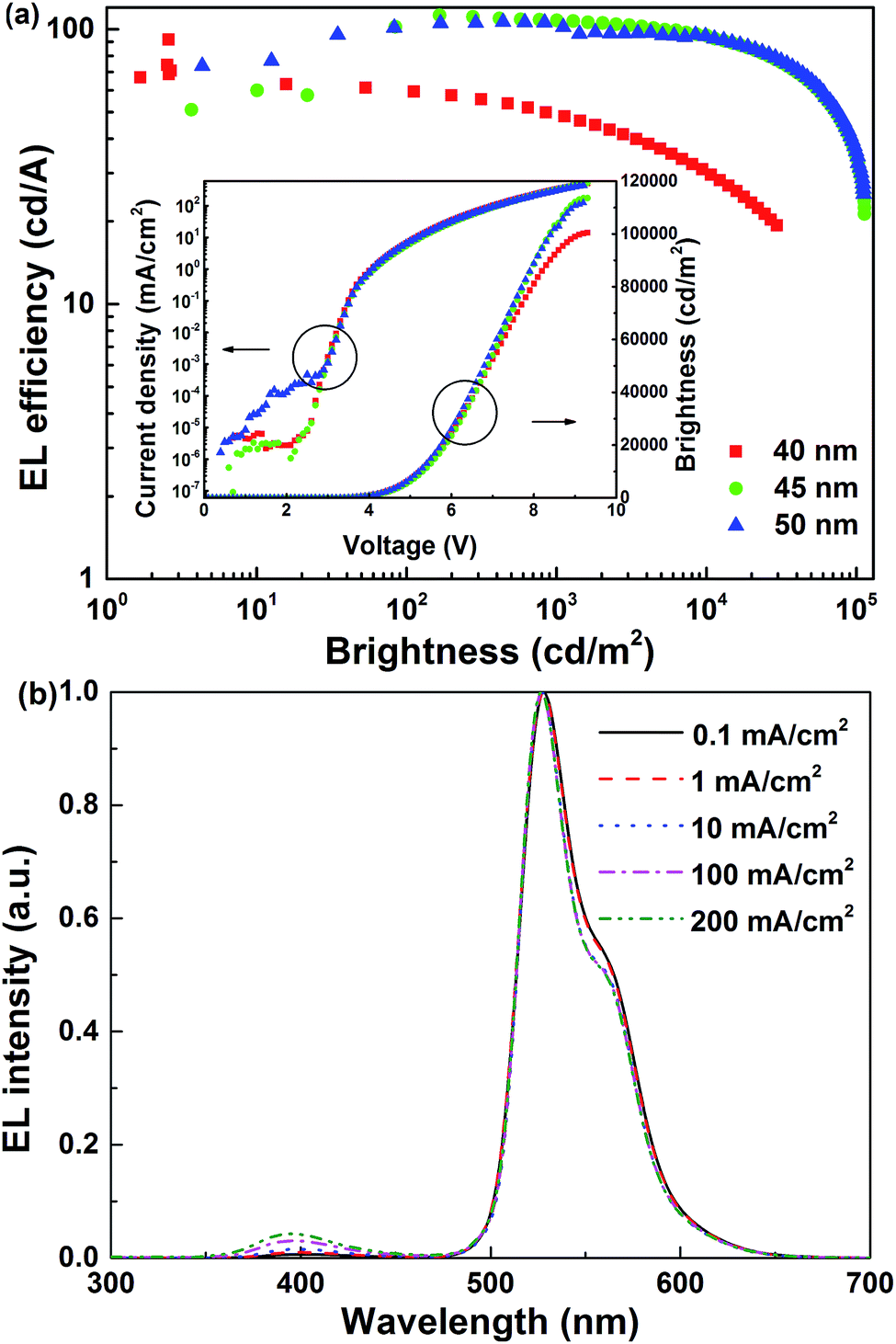 | ||
| Fig. 6 (a) EL efficiency–brightness (η–B) characteristics of the devices with different thicknesses of ETL. Insert: current density–brightness–voltage (J–B–V) characteristics of the devices with different thicknesses of ETL. (b) Normalized EL spectra of the device with 45 nm ETL operating at different current densities. | ||
| Device | Vturn-on (V) | Ba (cd m−2) | ηcb (EQEc) (cd A−1) | ηpd (lm W−1) | ηce (cd A−1) (EQEf) (1000 cd m−2) | CIEx,yg |
|---|---|---|---|---|---|---|
| a The data for maximum brightness (B).b Maximum current efficiency (ηc).c Maximum external quantum efficiency (EQE).d Maximum power efficiency (ηp).e Current efficiency (ηc) at the certain brightness of 1000 cd m−2.f External quantum efficiency (EQE) at the certain brightness of 1000 cd m−2.g Commission Internationale de l'Eclairage coordinates (CIEx,y) at 10 mA cm−2. | ||||||
| 40 nm | 3.2 | 100467 |
105.81 (26.9%) | 96.12 | 97.12 (24.7%, 4.1 V) | (0.294, 0.665) |
| 45 nm | 3.2 | 113610 |
112.30 (29.4%) | 97.95 | 107.60 (28.1%, 4.1 V) | (0.294, 0.662) |
| 50 nm | 3.2 | 111817 |
106.53 (26.5%) | 91.91 | 102.01 (25.3%, 4.1 V) | (0.298, 0.666) |
4. Conclusions
In this work, we have fabricated a series of devices with single- or double-EML(s) to further improve the EL performances of (tfmppy)2Ir(tpip) by selecting TcTa and 26DCzPPy as host materials due to their well matched energy levels. The broadening recombination zone of double-EMLs devices caused the relatively slower EL efficiency roll-off. To balance the distribution of holes and electrons, not only the doping concentration but also the thicknesses of EML2 and ETL were experimentally optimized. Finally, high performance green EL device with maximum brightness, current efficiency, power efficiency and EQE up to 113610 cd m−2, 112.30 cd A−1, 97.95 lm W−1 and 29.4%, respectively, was realized. Even at the practical brightness of 1000 cd m−2, current efficiency and EQE as high as 107.6 cd A−1 and 28.1%, respectively, can still be retained. To our best knowledge, EL performances of this device were amongst the highest results of the previously reported green devices.
Acknowledgements
The authors are grateful to the financial aid from Research Equipment Development Project of Chinese Academy of Sciences (YZ201562), Youth Innovation Promotion Association of Chinese Academy of Sciences (2013150), Strategic Priority Research Program of the Chinese Academy of Sciences (Grant No. XDB20030300), National Natural Science Foundation of China (21371093, 91433113, 21521092, 21590794 and 21210001), and National Key Basic Research Program of China (No. 2014CB643802 and 2013CB922101).References
- C. W. Tang, S. A. VanSlyke and C. H. Chen, J. Appl. Phys., 1989, 65, 3610 CrossRef CAS.
- M. A. Baldo, D. F. O'Brien, Y. You, A. Shoustikov, S. Sibley, M. E. Thompson and S. R. Forrest, Nature, 1998, 395, 151 CrossRef CAS.
- M. Schaer, F. Nüesch, D. Berner, W. Leo and L. Zuppiroli, Adv. Funct. Mater., 2001, 11, 116 CrossRef CAS.
- S. Reineke, F. Lindner, G. Schwartz, N. Seidler, K. Walzer, B. Lüssem and K. Leo, Nature, 2009, 459, 234 CrossRef CAS PubMed.
- J.-Y. Hu, Y.-J. Pu, F. Satoh, S. Kawata, H. Katagiri, H. Sasabe and J. Kido, Adv. Funct. Mater., 2014, 24, 2064 CrossRef CAS.
- C.-H. Yang, Y.-M. Cheng, Y. Chi, C.-J. Hsu, F.-C. Fang, K.-T. Wong, P.-T. Chou, C.-H. Chang, M.-H. Tsai and C.-C. Wu, Angew. Chem., Int. Ed., 2007, 46, 2418 CrossRef CAS PubMed.
- N. Sun, Q. Wang, Y. Zhao, Y. Chen, D. Yang, F. Zhao, J. Chen and D. Ma, Adv. Mater., 2014, 26, 1617 CrossRef CAS PubMed.
- Y. Seino, H. Sasabe, Y. J. Pu and J. Kido, Adv. Mater., 2014, 26, 1612 CrossRef CAS PubMed.
- Q. Wang, J. Ding, D. Ma, Y. Cheng, L. Wang, X. Jing and F. Wang, Adv. Funct. Mater., 2009, 19, 84 CrossRef CAS.
- S. Lamansky, P. Djurovich, D. Murphy, F. Abdel-Razzaq, H. E. Lee, C. Adachi, P. E. Bueeows, S. R. Forrest and M. E. Thompson, J. Am. Chem. Soc., 2001, 123, 4304 CrossRef CAS PubMed.
- J.-H. Jou, Y.-X. Lin, S.-H. Peng, C.-J. Li, Y.-M. Yang, C.-L. Chin, J.-J. Shyue, S.-S. Sun, M. Lee, C.-T. Chen, M.-C. Liu, C.-C. Chen, G.-Y. Chen, J.-H. Wu, C.-H. Li, C.-F. Sung, M.-J. Lee and J.-P. Hu, Adv. Funct. Mater., 2014, 24, 555 CrossRef CAS.
- Y.-C. Zhu, L. Zhou, H.-Y. Li, Q.-L. Xu, M.-Y. Teng, Y.-X. Zheng, J.-L. Zuo, H.-J. Zhang and X.-Z. You, Adv. Mater., 2011, 23, 4041 CrossRef CAS PubMed.
- J.-P. Duan, P.-P. Sun and C.-H. Cheng, Adv. Mater. Lett., 2003, 15, 224 CrossRef CAS.
- S. Lee, H. Shin and J.-J. Kim, Adv. Mater., 2014, 26, 5864 CrossRef CAS PubMed.
- W. S. Jeon, T. J. Park, S. Y. Kim, R. Pode, J. Jang and J. H. Kwon, Appl. Phys. Lett., 2008, 93, 063303 CrossRef.
- L. Zhou, Y. Zheng, R. Deng, J. Feng, M. Song, Z. Hao, H. Zhang, J. Zuo and X. You, J. Lumin., 2014, 148, 6 CrossRef CAS.
- L. Zhou, C.-C. Kwork, G. Cheng, H. Zhang and C.-M. Che, Opt. Lett., 2013, 38, 2373 CrossRef CAS PubMed.
- L. Zhou, C.-L. Kwong, C.-C. Kwok, G. Cheng, H. Zhang and C.-M. Che, Chem.–Asian J., 2014, 9, 2984 CrossRef CAS PubMed.
- J. Lee, N. Chopra, S.-H. Eom, Y. Zheng, J. Xue, F. So and J. Shi, Appl. Phys. Lett., 2008, 93, 123306 CrossRef.
- S.-J. Su, T. Chiba, T. Takeda and J. Kido, Adv. Mater., 2008, 20, 2125 CrossRef CAS.
- M. Ikai, S. Tokito, Y. Sakamoto, T. Suzuki and Y. Taga, Appl. Phys. Lett., 2001, 79, 156 CrossRef CAS.
- L. Xiao, Z. Chen, B. Qu, J. Luo, S. Kong, Q. Gong and J. Kido, Adv. Mater., 2011, 23, 926 CrossRef CAS PubMed.
- L. Zhou, H. Zhang, R. Deng, Z. Li, J. Yu and Z. Guo, J. Appl. Phys., 2007, 102, 064504 CrossRef.
- M. Uchida, C. Adachi, T. Koyama and Y. Taniguchi, J. Appl. Phys., 1999, 86, 1680 CrossRef CAS.
- I. D. Parker, J. Appl. Phys., 1993, 75, 1656 CrossRef.
| This journal is © The Royal Society of Chemistry 2016 |