
 Open Access Article
 This Open Access Article is licensed under a
 Creative Commons Attribution 3.0 Unported Licence
Graphene-porphyrin single-molecule transistors†
Jan A.
Mol‡
*a,
Chit Siong
Lau‡
a,
Wilfred J. M.
Lewis
b,
Hatef
Sadeghi
c,
Cecile
Roche
b,
Arjen
Cnossen
b,
Jamie H.
Warner
a,
Colin J.
Lambert
 c,
Harry L.
Anderson
b and
G. Andrew D.
Briggs
a
c,
Harry L.
Anderson
b and
G. Andrew D.
Briggs
a
aDepartment of Materials, University of Oxford, 16 Parks Road, Oxford OX1 3PH, UK. E-mail: jan.mol@materials.ox.ac.uk
bDepartment of Chemistry, University of Oxford, Chemistry Research Laboratory, Mansfield Road, Oxford OX1 3TA, UK
cQuantum Technology Centre, Physics Department, Lancaster University, LA1 4YB Lancaster, UK
First published on 10th July 2015
Abstract
We demonstrate a robust graphene-molecule-graphene transistor architecture. We observe remarkably reproducible single electron charging, which we attribute to insensitivity of the molecular junction to the atomic configuration of the graphene electrodes. The stability of the graphene electrodes allow for high-bias transport spectroscopy and the observation of multiple redox states at room-temperature.
Single molecules have long been heralded as the ultimate form of electronic device scaling.1,2 Harnessing the intrinsic functionality of individual molecules enables the bottom-up fabrication of atomically identical electronic building blocks.3–6 Contacting single molecules is a serious difficulty in single molecule electronics, because it requires scaleable and robust atomic-size electrodes that are energetically aligned with the molecular orbitals.7 A variety of fabrication approaches have been developed, including mechanical8 and electromigrated9 break-junctions and scanning probe techniques.10 Single-molecule rectifiers,3 transistors4 and switches5 have been experimentally demonstrated, and the read-out and manipulation of a single-molecule nuclear spin has been achieved.6 Despite these successful approaches the robustness and reproducibility of single-molecule contacts has remained an issue.11 Due to variability in their contacts, break-junction and scanning-probe approaches often rely on the repeated formation of thousands of metal-molecule junctions to infer information on the electronic properties of a single molecule.12
Carbon-based electrodes are appealing for contacting individual molecules.13,14 Unlike gold, which is the archetypical electrode materials for metal-molecule junctions, graphene has a low atomic mobility at room temperature, resulting in atomically stable electrodes.15 While different metals with a lower atomic mobility might also provide stable electrodes,16 the workfunction of these metals are typically not well matched to the discrete energy levels of the molecule as is the case for graphene.17 Furthermore, the two-dimensional nature of graphene results in weaker screening of a gate electric field compared to bulky three-dimensional electrodes, which means the distance between the gate electrode can be much larger than the distance between the source and drain electrodes whilst still maintaining the capability of gating the molecular orbitals. Here we demonstrate a robust graphene-molecule-graphene contacting geometry where a stable and reproducible single-molecule single-electron transistor (SET) architecture is achieved through careful design of the molecular building blocks and controlled formation of graphene nanogaps.
Modular molecular designs, consisting of a molecular backbone with specific side-groups for anchoring, spacing and self-alignment, in combination with graphene electrodes, have been proposed to overcome the variability issues that have long limited single-molecule electronics.7,18 Orbital gating of small molecules anchored to graphene electrodes has been demonstrated,15 but, to date, there are no studies of charge transport through complex modular molecules coupled to graphene electrodes. In this work, we study the charge transport through individual molecules in a graphene-molecule-graphene junction. The molecular wire, shown in Fig. 1a, consists of a zinc-porphyrin back-bone (black in Fig. 1a) with tetrabenzofluorene anchors (green in Fig. 1a). Porphyrin molecules provide a versatile platform for molecular device functionality,19 and have been widely investigated as such.20–22 Anchoring the molecular backbone to the graphene electrodes can be achieved either by covalent C–C bonding,23 or by π–π-stacking.15 The latter is especially of interest, as it leaves the electronic structure of the molecule largely unchanged, in contrast to thiol anchors which introduce gap-type states.24 Tetrabenzofluorene (TBF) ‘butterfly’ anchor groups used in this study are known to bind strongly to graphite surfaces25 and carbon nanotubes,26 and are robust in solvent solution.25 Density functional theory (DFT) calculations shown in Fig. 1b reveal that there is no steric hindrance to adsorption, and that the molecular wire relaxes across the graphene nanogap in a planar geometry. DFT calculations further indicate that the wavefunctions of the highest occupied molecular orbital (HOMO) are delocalised over the porphyrin backbone and anchor groups in contrast to the lowest unoccupied molecular orbital (LUMO) which are only localised over the porphyrin backbone, as shown in Fig. 1c. Overlap between the delocalised electron wavefunctions of the fully conjugated zinc-porphyrin system with the butterfly anchors allows for electron transport through the wire. The molecular backbone is separated from the butterfly anchor groups by a spacer (blue in Fig. 1a), which allows the anchor groups to bind to the defect-free graphene rather than to the graphene edges. In addition to the butterfly limpets, the molecule has two bulky side-groups (red in Fig. 1a). The side-groups make the molecular wire more soluble and prevent the central porphyrin from binding to the graphene electrodes.
 | ||
| Fig. 1 (a) Chemical structure of the molecular wire with a zinc-porphyrin backbone (black), ‘butterfly’ anchor groups (green) and bulky side groups (red). The functional groups allow for a robust, self aligning mechanism. (b) Schematic of the single-molecule transistor. A heavily doped silicon chip with a 300 nm silicon oxide layer is used as a back gate to modulate charge transport through the device. (c) DFT simulations of LDOS for HOMO and LUMO iso-surfaces. (d) Typical 4 K current–voltage (I–V) trace before (blue) and after (red) depositing molecules. The observed increase in current after exposing the nanogaps to the porphyrin solution is representative for all devices measured. The inset shows a false-color scanning electron micrograph of the device. The scale bar is 1 μm. | ||
We used lithographically patterned chemical vapour deposited (CVD) single-layer graphene,27,28 resulting in devices with greater reproducibility than those fabricated from few-layer graphene flakes.15 The graphene electrodes are fabricated using feedback-controlled electroburning28,29 and are typically separated by 1–2 nm. The chemical potential of the molecular wire is electrostatically tuned using the conducting silicon substrate as a back-gate (see Fig. 1b), which is separated from the molecule and graphene electrodes by a 300 nm thick silicon-oxide layer, resulting in a SET device geometry. The graphene electrodes are stable in air for at least several days. Molecules are deposited from a chloroform solution, after which the samples are immediately transferred into vacuum to prevent contamination. Fig. 1d shows typical current-voltage traces before (blue) and after (red) deposition of the molecule measured at 4 K. Before deposition of the molecule the current shows smooth exponential behaviour indicative of tunnelling through a single barrier. After deposition the presence of a molecule results in stepwise increases of the current as expected for sequential tunnelling through a double-barrier system. A scanning electron micrograph image of the device is shown in the inset of Fig. 1d.
First, we demonstrate reproducible single-electron transport through individual molecules. We show that the single electron charging is determined by the molecule rather than the microscopic details of the electrodes. Reproducible SET behaviour is measured in 10 out of 48 devices at 20 mK on which we deposited the molecular wire described above, as shown in Fig. 2. We find that for all devices Eadd = 0.37 ± 0.05 eV for the Coulomb diamond closest to equilibrium (zero gate voltage). The device statistics presented in Table 1 indicate that the measured SET behaviour of the devices shown in Fig. 2 arises from charge transport through approximately identical single-molecule transistors. In a control experiment using the same molecular backbone but without the TBF limpets (see Fig. SI2†), 20 devices were tested and no Coulomb diamonds were observed. From the reproducibility and from the control experiment we deduce: (i) molecules attach to the electrodes only when they are functionalised with anchor groups; (ii) the SET behaviour can be attributed to a molecule bridging the gap; (iii) the SET behaviour cannot be attributed to multiple molecules or to random carbon islands. The presence of multiple molecules would lead to multiple overlapping Coulomb diamonds whereas carbon islands would be expected to give more variable energy spacing Eadd. The observation of a constant energy spacing of Eadd ≈ 0.37 V for 10 out of 12 of the devices displaying Coulomb diamonds is a clear indication that there is only one active molecule in each device.
 | ||
| Fig. 2 The source-drain current I as a function of source-drain bias Vb and gate voltage Vg. All devices shown are in the weak-coupling regime where the current I ∼ pA–nA, meaning that an electron tunnels from the source electrode to the molecule, and then on to the drain, in a sequential process. Sequential electron tunnelling leads to diamond shaped regions where charge transport is Coulomb blocked. All devices were measured at 20 mK. | ||
| E add < 0.1 | E add ≈ 0.37 | No CB | |
|---|---|---|---|
| TBF anchors | 2 | 10 | 36 |
| No anchors | 0 | 0 | 20 |
A residual degree of variability is still present in the molecular devices. The horizontal axes in Fig. 2 are scaled by an effective lever arm α which is a measure of the capacitive coupling between the gate and the molecule, and differs from device to device, with α = 0.006 − 0.04 estimated from the slopes of the Coulomb diamonds. The gate coupling observed in our devices with a 300 nm thick oxide are comparable to those reported for metal junctions on an oxide with a thickness of 40 nm.30 The small values of α indicate that the total capacitance is dominated by the source and drain electrodes, and is consistent with electrostatic calculations (ESI.II.C†). The variation in α can be attributed to differences in screening of the gate-field by the source and drain electrodes. The gate voltage to align the electrochemical potential of the electrodes with the Dirac point is greater than 40 V, thus giving an upper limit to the shift in the electrochemical potential of the electrodes as less than half the change in the potential of the molecule deduced from the slope of the Coulomb diamonds (ESI.II.D†). Trap states in the form of defects in the gate-oxide that can capture an electron and adsorbants on the graphene electrodes give rise to shifted and non-closing Coulomb diamonds (ESI.II.E†). Finally, we observe a significant variation in the current through the single-molecule devices, which can be attributed to differences in overlap between the anchor-groups and the graphene electrodes.
By looking more accurately at the transport spectroscopy of device 8, we can obtain the level spacing of the molecular orbitals and electron–electron interactions in the molecule. The stability of our molecular system (Fig. 3a) allows us to measure the energy spacing Eadd(N) between the ground state (GS) transitions from redox state N to redox state N + 1 of the molecule, from the height of the Coulomb diamonds. In the constant interaction model the addition energy consists of two parts:31 (i) the charging energy EC, due to the Coulomb interactions among electrons in the molecule and between electrons in the molecule and those in the environment; and (ii) the gap ΔHL between the HOMO and LUMO energy-levels. We can estimate the contribution of ΔHL and EC to the addition energy by comparing Eadd(N) for successive redox states and considering the spin-degeneracy of the molecular orbitals. We find that ΔHL = 0.05 eV for the N − 2 redox state and ΔHL = 0.06 eV for the N redox state. Several redox states have been observed in previous work on OPV molecules in gold nanogaps.4 The interpretation of the different contributions to Eadd can be further substantiated by comparing ΔHL with the single-particle energy level spacing which can be determined from the excited state spectrum for each redox state (see Fig. 3c). The stability of graphene allows us to extend measurements to bias-voltages beyond the limit set by electromigration for gold electrodes.4 We find that the first excited state of the N − 2 redox state aligns closely with the ground state of the N − 1 and N redox states. Likewise, the second excited state of N − 2 redox state aligns with the first excited state of N − 1 and N and the ground state of the N + 1 and N + 2 redox states. The single-electron energy spectrum seems to be largely independent of the number of electrons, with intervals dominated by the HOMO–LUMO energy separation. Renormalisation corrections of ∼3–4 eV have been observed experimentally and predicted theoretically for molecules in nanogaps32 and for molecules on graphite surfaces.33 For unscreened gas phase molecules our calculations yield an addition energy for one electron Eadd = 3.84 eV. From a simple screening potential (see ESI.III†) we estimate the reduction of the addition energy to be of the order of 3 eV, which is in reasonable agreement with our experimental findings.
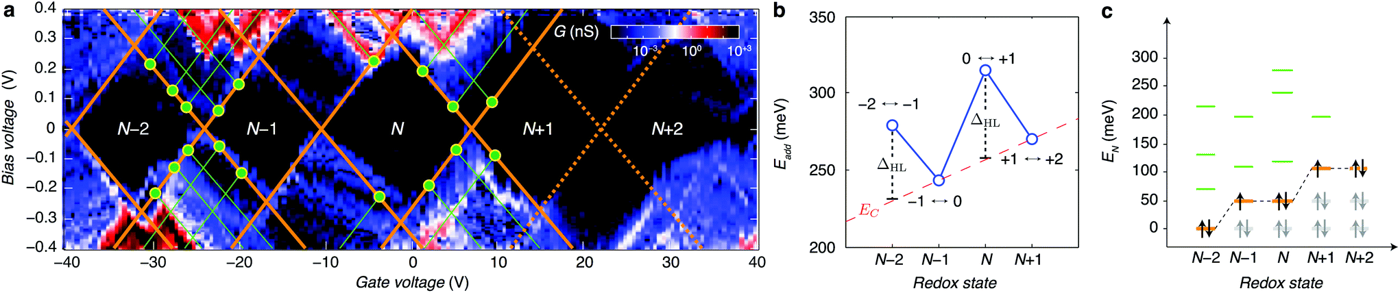 | ||
| Fig. 3 (a) Differential conductance dI/dVg (on a logarithmic scale) as a function of Vb and Vg. The excited state spectrum is measured from the source/drain conductance. Excited state transitions result in lines in the differential conductance diagram running parallel to the edges of the Coulomb diamonds. The bias voltage where an excited state line intersects the Coulomb blockade region (indicated by the green dots in a) is a direct measure of the excited state energy EN, i = e|Vb, i|, where EN, i is the energy of ith excited state with respect to the ground state for the Nth redox state. The N + 1 ↔ N + 2 transition appears to be suppressed (dashed lines), the charge degeneracy point for this transition is inferred from the features in the bottom-right of the N + 1 diamond and the top-left of the N + 2 diamond. (b) Addition energy as a function the redox state N. The HOMO–LUMO gap ΔHL is estimated from the energy difference in odd-even filling. For a redox state with an even number of electrons in the molecule, the HOMO is fully occupied and the additional electron will occupy the LUMO which is separated from the HOMO by the single-particle energy-level spacing ΔHL. We identify the two high-energy transitions as the even ↔ odd transitions where Eadd(N) = EC + ΔHL and the low-energy as the odd ↔ even transitions where Eadd(N) = EC. The charging energy EC(N) = EC0 + βN with EC0 = 0.23 eV β = 0.01 eV is estimated from a linear interpolation of Eadd(N − 1) and Eadd(N + 1). (c) Single-particle energy spectrum as a function of redox state N. Using the values for ΔHL and the excited state spectra for each redox state an orbital-filling diagram is constructed. Starting from the N − 2 redox state, the successive ground state energy level is found by adding ΔHL, resulting in the orange lines in c. Next the excited state energies EN, i are added to the ground state energy for each redox state, resulting in the green lines in c. | ||
Finally, we discuss the room temperature operation of the graphene-molecule-graphene transistors. Fig. 4 shows the stability diagram of device 2 measured at room temperature. Two Coulomb diamonds can be fully resolved, allowing us to probe the charge state transitions between three successive redox states. Using the same methodology as describe above we can estimate the charging energy EC = 0.28 ± 0.05 eV and HOMO–LUMO gap ΔHL = 0.09 ± 0.05 eV by comparing Eadd of the N and N + 1 redox states measured at room temperature.
 | ||
| Fig. 4 Current stability diagram as a function of Vb and Vg measured at room temperature. We attribute the shift in the Coulomb diamonds with respect to the 20 mK data to thermal activation of offset charges in the oxide. | ||
In conclusion, we have demonstrated room-temperature charge- and energy-quantization in a reproducible graphene-molecule-graphene device geometry. The modular design of the molecular wire makes this approach applicable to a wide variety of molecular backbones. Specifically, the π–π anchoring of the molecule to the highly stable graphene nano-electrodes allows high-bias energy spectroscopy of the excited states and removes the need for statistical analysis of ensemble measurements. Our findings offer a route to a vast number of quantum transport experiments that are well established for semiconductor quantum dots, but at an energy-scale larger than kT at room temperature.
An approach that combines single molecules with novel two-dimensional materials and semiconductor fabrication technologies forms an attractive platform with which to realise scalable room-temperature single-electron transistor networks. Such an architecture could consist of individual molecules coupled to each other via graphene leads, with nearby graphene gate-electrodes to tune the orbital energy levels of the individual molecules. The gate-electrodes could be separated from the molecules by a two-dimensional insulator, to enable strong capacitive coupling between the gate and the molecule and allow the single-molecule transistors to exhibit gain. Here we have demonstrated the first step towards such an architecture: a reproducible single-molecule transistor. Further improvements in the graphene nanogap fabrication need to be made to reduce the offset charges and eliminate variability in the gate coupling as discussed above, providing a basis for the development of single-molecule electronics and also applicable to the fabrication of single-molecule based sensors and spin-based quantum computation.
Acknowledgements
We thank the Royal Society for a Newton International Fellowship for J. A. M. and a University Research Fellowship for J. H. W., and the Agency for Science Technology and Research (A*STAR) for a studentship for C. S. L. This work is supported by Oxford Martin School, EPSRC grants EP/J015067/1, EP/K001507/1, EP/J014753/1, EP/H035818/1, and the European Union Marie-Curie Network MOLESCO. This project/publication was made possible through the support of a grant from Templeton World Charity Foundation. The opinions expressed in this publication are those of the author(s) and do not necessarily reflect the views of Templeton World Charity Foundation.References
- A. Aviram and M. A. Ratner, Chem. Phys. Lett., 1974, 29, 277–283 CrossRef CAS.
- S. V. Aradhya and L. Venkataraman, Nat. Nanotechnol., 2013, 8, 399–410 CrossRef CAS PubMed.
- R. M. Metzger, B. Chen, U. Höpfner, M. V. Lakshmikantham, D. Vuillaume, T. Kawai, X. Wu, H. Tachibana, T. V. Hughes, H. Sakurai, J. W. Baldwin, C. Hosch, M. P. Cava, L. Brehmer and G. J. Ashwell, J. Am. Chem. Soc., 1997, 119, 10455–10466 CrossRef CAS.
- S. Kubatkin, A. Danilov, M. Hjort, J. Cornil, J.-L. Brédas, N. Stuhr-Hansen, P. Hedegård and T. Bjørnholm, Nature, 2003, 425, 698–701 CrossRef CAS PubMed.
- S. Y. Quek, M. Kamenetska, M. L. Steigerwald, H. J. Choi, S. G. Louie, M. S. Hybertsen, J. B. Neaton and L. Venkataraman, Nat. Nanotechnol., 2009, 4, 230–234 CrossRef CAS PubMed.
- S. Thiele, F. Balestro, R. Ballou, S. Klyatskaya, M. Ruben and W. Wernsdorfer, Science, 2014, 344, 1135–1138 CrossRef CAS PubMed.
- E. Lörtscher, Nat. Nanotechnol., 2013, 8, 381–384 CrossRef PubMed.
- C. Bruot, J. Hihath and N. Tao, Nat. Nanotechnol., 2011, 7, 35–40 CrossRef PubMed.
- W. Liang, M. P. Shores, M. Bockrath, J. R. Long and H. Park, Nature, 2002, 417, 725–729 CrossRef CAS PubMed.
- C. M. Guédon, H. Valkenier, T. Markussen, K. S. Thygesen, J. C. Hummelen and S. J. van der Molen, Nat. Nanotechnol., 2012, 7, 305–309 CrossRef PubMed.
- G. Schull, T. Frederiksen, A. Arnau, D. Sánchez-Portal and R. Berndt, Nat. Nanotechnol., 2010, 6, 23–27 CrossRef PubMed.
- B. Xu, Science, 2003, 301, 1221–1223 CrossRef CAS PubMed.
- X. Guo, J. P. Small, J. E. Klare, Y. Wang, M. S. Purewal, I. W. Tam, B. H. Hong, R. Caldwell, L. Huang, S. O'Brien, J. Yan, R. Breslow, S. J. Wind, J. Hone, P. Kim and C. Nuckolls, Science, 2006, 311, 356–359 CrossRef CAS PubMed.
- C. W. Marquardt, S. Grunder, A. Baszczyk, S. Dehm, F. Hennrich, H. von Löhneysen, M. Mayor and R. Krupke, Nat. Nanotechnol., 2010, 5, 863–867 CrossRef CAS PubMed.
- F. Prins, A. Barreiro, J. W. Ruitenberg, J. S. Seldenthuis, N. Aliaga-Alcalde, L. M. K. Vandersypen and H. S. J. van der Zant, Nano Lett., 2011, 11, 4607–4611 CrossRef CAS PubMed.
- F. Prins, T. Hayashi, B. J. A. de Vos van Steenwijk, B. Gao, E. A. Osorio, K. Muraki and H. S. J. van der Zant, Appl. Phys. Lett., 2009, 94, 123108 CrossRef PubMed.
- C. Jia and X. Guo, Chem. Soc. Rev., 2013, 42, 5642 RSC.
- C. G. Péterfalvi and C. J. Lambert, Phys. Rev. B: Condens. Matter, 2012, 86, 085443 CrossRef.
- M. L. Perrin, F. Prins, C. A. Martin, A. J. Shaikh, R. Eelkema, J. H. van Esch, T. Briza, R. Kaplanek, V. Kral, J. M. van Ruitenbeek, H. S. J. van der Zant and D. Dulić, Angew. Chem., Int. Ed., 2011, 50, 11223–11226 CrossRef CAS PubMed.
- M. Jurow, A. E. Schuckman, J. D. Batteas and C. M. Drain, Coord. Chem. Rev., 2010, 254, 2297–2310 CrossRef CAS PubMed.
- S. Mohnani and D. Bonifazi, Coord. Chem. Rev., 2010, 254, 2342–2362 CrossRef CAS PubMed.
- G. Sedghi, V. M. Garcia-Suarez, L. J. Esdaile, H. L. Anderson, C. J. Lambert, S. Martin, D. Bethell, S. J. Higgins, M. Elliott, N. Bennett, J. E. Macdonald and R. J. Nichols, Nat. Nanotechnol., 2011, 6, 517–523 CrossRef CAS PubMed.
- Y. Cao, S. Dong, S. Liu, L. He, L. Gan, X. Yu, M. L. Steigerwald, X. Wu, Z. Liu and X. Guo, Angew. Chem., Int. Ed., 2012, 51, 12228–12232 CrossRef CAS PubMed.
- M. L. Perrin, C. J. O. Verzijl, C. A. Martin, A. J. Shaikh, R. Eelkema, J. H. van Esch, J. M. van Ruitenbeek, J. M. Thijssen, H. S. J. van der Zant and D. Dulić, Nat. Nanotechnol., 2013, 8, 282–287 CrossRef CAS PubMed.
- J. K. Dutton, J. H. Knox, X. Radisson, H. J. Ritchie and R. Ramage, J. Chem. Soc., Perkin Trans. 1, 1995, 2581 RSC.
- M. Assali, M. P. Leal, I. Fernández, P. Romero-Gomez, R. Baati and N. Khiar, Nano Res., 2010, 3, 764–778 CrossRef CAS.
- Y. A. Wu, Y. Fan, S. Speller, G. L. Creeth, J. T. Sadowski, K. He, A. W. Robertson, C. S. Allen and J. H. Warner, ACS Nano, 2012, 6, 5010–5017 CrossRef CAS PubMed.
- C. S. Lau, J. A. Mol, J. H. Warner and G. A. D. Briggs, Phys. Chem. Chem. Phys., 2014, 20398–20401 RSC.
- H. Sadeghi, J. A. Mol, C. S. Lau, G. A. D. Briggs, J. Warner and C. J. Lambert, Proc. Natl. Acad. Sci. U. S. A., 2015, 112, 2658–2663 CrossRef CAS PubMed.
- M. L. Perrin, E. Burzurí and H. S. J. van der Zant, Chem. Soc. Rev., 2015, 44, 902–919 RSC.
- K. Kaasbjerg and K. Flensberg, Nano Lett., 2008, 8, 3809–3814 CrossRef CAS PubMed.
- K. Moth-Poulsen and T. Bjørnholm, Nat. Nanotechnol., 2009, 4, 551–556 CrossRef CAS PubMed.
- J. B. Neaton, M. S. Hybertsen and S. G. Louie, Phys. Rev. Lett., 2006, 97, 216405 CrossRef CAS.
Footnotes |
| † Electronic supplementary information (ESI) available. See DOI: 10.1039/C5NR03294F |
| ‡ These authors contributed equally to this work. |
| This journal is © The Royal Society of Chemistry 2015 |