
A multiple negative differential resistance heterojunction device and its circuit application to ternary static random access memory†
Kwan-Ho
Kim‡
a,
Hyung-Youl
Park‡
a,
Jaewoo
Shim
b,
Gicheol
Shin
c,
Maksim
Andreev
a,
Jiwan
Koo
a,
Gwangwe
Yoo
a,
Kilsu
Jung
a,
Keun
Heo
a,
Yoonmyung
Lee
c,
Hyun-Yong
Yu
d,
Kyung Rok
Kim
e,
Jeong Ho
Cho
 f,
Sungjoo
Lee
ag and
Jin-Hong
Park
*ag
f,
Sungjoo
Lee
ag and
Jin-Hong
Park
*ag
aDepartment of Electrical and Computer Engineering, Sungkyunkwan University, Suwon 16419, Korea. E-mail: jhpark9@skku.edu
bDepartment of Mechanical Engineering, Massachusetts Institute of Technology (MIT), Cambridge, MA 02139, USA
cDepartment of Semiconductor System Engineering, Sungkyunkwan University, Suwon 16419, Korea
dSchool of Electrical Engineering, Korea University, Seoul 02841, Korea
eSchool of Electrical and Computer Engineering, Ulsan National Institute of Science and Technology (UNIST), Ulsan 44919, Korea
fDepartment of Chemical and Biomolecular Engineering, Yonsei University, Seoul 03722, Korea
gSKKU Advanced Institute of Nanotechnology (SAINT), Sungkyunkwan University, Suwon 16419, Korea
First published on 24th January 2020
Abstract
For increasing the restricted bit-density in the conventional binary logic system, extensive research efforts have been directed toward implementing single devices with a two threshold voltage (VTH) characteristic via the single negative differential resistance (NDR) phenomenon. In particular, recent advances in forming van der Waals (vdW) heterostructures with two-dimensional crystals have opened up new possibilities for realizing such NDR-based tunneling devices. However, it has been challenging to exhibit three VTH through the multiple-NDR (m-NDR) phenomenon in a single device even by using vdW heterostructures. Here, we show the m-NDR device formed on a BP/(ReS2 + HfS2) type-III double-heterostructure. This m-NDR device is then integrated with a vdW transistor to demonstrate a ternary vdW latch circuit capable of storing three logic states. Finally, the ternary latch is extended toward ternary SRAM, and its high-speed write and read operations are theoretically verified.
Introduction
As very-large-scale integration technology progresses to the few-nanometer scale, the interconnect lines are becoming thinner and longer. This increases the parasitic resistances and capacitances, causing excessive power consumption and long signal delays in integrated chips.1,2 To address these issues, multi-valued logic (MVL) using more than three logic states (“0”, “1”, “2”, etc.) has recently been explored.3,4,12–14,31–33,53–56 In MVL-based processing systems, fewer devices and interconnect lines are needed for processing the same amount of data compared with the conventional binary logic system, which allows the power dissipation and signal delay in the interconnect region to be reduced.34,35 Recently, to implement unit circuits for such an MVL system, tunneling devices exhibiting the negative differential resistance (NDR) phenomenon have been reconsidered.4–9,20,21 Owing to the N-shaped current–voltage (I–V) characteristic of these NDR tunneling devices, multiple threshold voltages (multi-VTH) exist in a single device, which allows for two or more electrically stable operating points during the circuit operation; with n successive NDR current peaks, n + 1 stable operating points and n + 1 corresponding logical states can be designed in MVL circuits.30–33The practical realization of such NDR tunneling devices imposes rigorous requirements on the junction quality. The low interfacial defect density and atom-scale sharpness at the junction are essential for the fabrication of the device.7,12,19 Beyond III–V compound heterojunction structures, recent advances in forming van der Waals (vdW) heterostructures with two-dimensional (2D) crystals, such as molybdenum disulfide (MoS2), black phosphorus (BP), rhenium disulfide (ReS2), and hafnium disulfide (HfS2), have introduced new possibilities for realizing NDR tunneling devices and even MVL circuits.3–7,13–27,49–52,58 Because 2D vdW crystals have fewer defects on the surface compared to conventional crystal materials, superior heterojunctions with interfaces that are atomically sharp and have low density of defects can be formed without the lattice mismatch constraint.10,11 By stacking 2D vdW crystals of h-BN and graphene alternately, L. Britnell et al. and A. Mishchenko et al. developed graphene/h-BN/graphene heterojunction-based resonant tunneling diodes exhibiting the NDR phenomenon.5,6 In these devices, the Fermi levels of the graphene layers were separately controlled using additional gate terminals, allowing resonant tunneling transport between the graphene layers through the h-BN. Another type of tunneling NDR device was reported by Yan et al.15 In that study, to achieve the NDR phenomenon, a type-III heterojunction with a broken energy bandgap was formed by stacking two vdW crystal materials with non-overlapping energy bandgaps. Subsequently, the n+/p+ heterojunction obtained without chemical or electrical doping allowed the band-to-band tunneling (BTBT) transport. Although the NDR phenomenon has been successfully achieved in several vdW heterojunctions, the demonstration of MVL devices/circuits using the NDR characteristics has been challenging. Recently, Shim et al. showed the feasibility of an MVL circuit (ternary inverter) by connecting a p-channel transistor to an NDR device in series.4 However, the presented logic states were not stable, because this tunneling device had only a single NDR phenomenon, which can provide at most two stable operating points. For the successful implementation of MVL circuits with stable logic states, it is very important to implement the multiple-NDR (m-NDR) phenomenon in a single vdW tunneling device, which is physically challenging and has not yet been observed thus far.
Here, we report the m-NDR phenomenon implemented in a single vdW tunneling device fabricated on a BP/(ReS2 + HfS2) type-III double-heterojunction structure. To achieve this m-NDR characteristic, we used the principle that the tunneling currents through the BP/ReS2 and BP/HfS2 junctions are blocked by the BP bandgap at different bias points. We focused on the analysis of the energy band of the double heterojunction via microbeam X-ray photoelectron spectroscopy (μ-XPS). On the basis of the determined band structure, we discussed the operating mechanism of the vdW tunneling device from the perspective of the tunneling and diffusion phenomena. Then, by integrating the vdW tunneling device and a p-channel vdW transistor in series, we demonstrated a ternary latch circuit capable of storing three logic states. Furthermore, this ternary latch circuit was extended toward ternary static random-access memory (SRAM), and its write and read operations were theoretically verified by using a Cadence Spectre simulator.
Results and discussion
Fig. 1a presents a schematic of the BP/(ReS2 + HfS2) type-III double heterojunction. We started the junction fabrication process by exfoliating BP, ReS2, and HfS2 crystal flakes onto a clean substrate using a tape-based exfoliation method. The flakes were then picked up by using a polymer substrate with a stronger adhesion force than that between the 2D crystal flakes and the substrate, and those were finally transferred to the desired region of a SiO2/Si substrate (this transfer process is described in detail in Fig. S1, ESI†). As shown in Fig. 1b, the double heterojunction was examined using cross-sectional transmission electron microscopy (X-TEM) and energy-dispersive X-ray spectroscopy (EDS). The thickness of the BP flake was approximately 118 nm, whereas the thicknesses of the ReS2 and HfS2 flakes were estimated to be approximately 26 nm (Fig. S11, ESI†). We observed a void space between the ReS2 and the HfS2, which electrically separated the BP/ReS2 and BP/HfS2 type-III heterojunctions. Even if the thickness of the BP is reduced to 7 nm, the void space in the BP/(ReS2 + HfS2) double-heterostructure would be retained because the elastic modulus of BP barely decreases until the thickness of BP is reduced to 7 nm.57 The flakes were subjected to atomic composition analysis through EDS mapping, where the top region mainly showed a P signal (purple), and signals corresponding to Re (blue) and Hf (green) were obtained in the two bottom regions. The signal from S atoms is shown in Fig. S2 (ESI†). The high-resolution transmission electron microscopy (TEM) images shown in Fig. 1c indicate that the heterojunctions had clean and abrupt junction interfaces. An amorphous phase was observed in the BP region near the junction interface (marked by an orange dotted line), but the EDS mapping indicates that the amorphous layer was not the result of alloying with adjacent layers or polymer residuals (Fig. S3, ESI†). Probably, owing to the instability of BP in air, the amorphous BP layer was formed by oxidation during the transfer process.17,28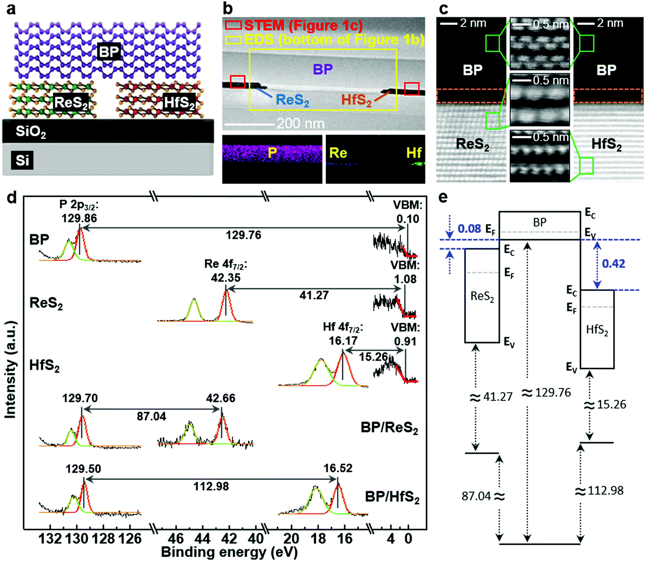 | ||
| Fig. 1 Analysis of the type-III double heterojunction. (a) Schematic illustration of the BP/(ReS2 + HfS2) type-III double heterojunction. (b) Cross-sectional transmission electron microscopy (X-TEM) image of the double heterojunction (top) and energy-dispersive X-ray spectroscopy (EDS) mapping of phosphorus (P) atoms (bottom left image), and rhenium (Re) and hafnium (Hf) atoms (bottom right image). (c) High-resolution transmission electron microscopy (HRTEM) images of BP/ReS2 and BP/HfS2 heterojunctions. (d) Core-level spectra of individual materials (BP, ReS2, HfS2) and heterojunctions (BP/ReS2 and BP/HfS2) obtained from micro-beam X-ray photoelectron spectroscopy (μ-XPS). (e) Band alignments of the BP/(ReS2 + HfS2) type-III double heterojunction that is predicted from core-level analysis. | ||
We also performed μ-XPS measurements on the BP/(ReS2 + HfS2) double heterojunction to investigate its energy band alignment in detail. Detailed information regarding this measurement is shown in Fig. S4 (ESI†). Through the analysis of (i) core-level (CL) spectra from individual materials and (ii) CL spectra from the heterojunctions, we predicted the valence-band offsets (VBOs) of the double-heterojunction structure.36–39Fig. 1d shows the CL spectra for P 2p, Re 4f, Hf 4f, P 2p + Re 4f, and P 2p + Hf 4f, as well as the valence-band maximum (VBM), where we found the binding energies. By inserting the binding energy and VBM values into the following equation, the VBO values for the BP/ReS2 and BP/HfS2 junctions were calculated as 1.45 and 1.52 eV, respectively:
| VBOBP/MS2 = (EBP − EBPVBM) − (EMS2 − EMS2VBM) − (EBP/MS2 − EBP/MS2) |
| (Broken-gap)BP/MS2 = VBOBP/MS2 − Eg,MS2 |
The broken energy gaps for BP/ReS2 and BP/HfS2 were 0.08 and 0.42 eV, respectively. In this calculation, we referred to the bandgap values (0.39 eV for BP, 1.37 eV for ReS2, and 1.1 eV for HfS2) theoretically predicted via first-principle calculations.4,43–46 The broken gap of the BP/ReS2 heterojunction obtained via μ-XPS measurements was close to the value (0.09 eV) theoretically estimated in Fig. S5 (ESI†), but that of the BP/HfS2 junction was smaller than its theoretical value (1 eV). We confirmed that the CL spectra peaks observed in the BP/ReS2 and BP/HfS2 heterojunctions slightly shifted from the peaks of the individual materials. After the formation of the heterojunctions, the P 2p CL peaks moved toward lower binding energies (by 0.16 eV at BP/ReS2 and 0.36 eV at BP/HfS2), while the Re 4f and Hf 4f CL peaks shifted to higher binding energies (by 0.31 and 0.35 eV, respectively) (Fig. S6, ESI†). This peak-shift appears to be caused by the charge transfer from BP to ReS2 and HfS2.39–42 Because the relatively low work function of BP allows a large number of electrons to be transferred from BP to ReS2 and HfS2, the Fermi level at the BP-side junction interface is predicted to move under the valence band edge, reducing the P 2p CL peak binding energy. In contrast, the shift of the Re 4F and Hf 4f CL peaks to higher binding energies can be explained by the downward band bending at the ReS2- and HfS2-side junction interface after the electrons were received from the BP. Generally, the shift of the CL spectra peak provides information regarding the energy band bending, because the peak position in the CL spectra indicates the difference between the Fermi energy level and the core energy level.39–42
We then implemented a vertical tunneling device on the BP/(ReS2 + HfS2) double heterojunction, as shown in Fig. 2a. In this device, two distinct current paths existed between the anode and cathode: one path passed through the BP/ReS2 heterojunction, and the other was on the BP/HfS2 heterojunction. Fig. 2b shows the energy band structures of the heterojunctions in the thermal equilibrium state. As predicted by the CL peak shifts (Fig. 1d), the interface regions of both BP/ReS2 and BP/HfS2 junctions were expected to be degenerately doped without the assistance of doping techniques. Because such highly doped junctions near the interfaces are similar to the Esaki diode junction exhibiting the NDR phenomenon,29 as shown in Fig. 2c, two consecutive NDR phenomena were confirmed in this device. The first and second NDR peaks were observed at 0.76 and 1.10 V, respectively. In particular, the peak and valley currents appeared at similar voltage points during repeated measurements, as shown in Fig. 2d. The current-transport mechanism of this device is qualitatively explained in detail in Fig. 2e–h. The overall operating mechanism was based on tunneling and diffusion phenomena, which contributed differently to the total current according to the applied voltage range. At a small-voltage bias region, electrons in conduction bands of ReS2 and HfS2 moved to the empty valence-band states of BP through the BTBT transport. The magnitude of BTBT increased with the applied voltage, increasing the tunneling current. As the voltage bias increased, the tunneling current increased and reached its first maximum level when the Fermi level of ReS2 was aligned with the VBM of BP. Then, the tunneling current abruptly decreased, exhibiting the first NDR at 0.76 V, because the electrons were unable to tunnel into the bandgap of BP from ReS2. A further increase in voltage caused the total current to increase again via high electron tunneling at the BP/HfS2 junction, and then the second NDR appeared at 1.10 V when the Fermi level of HfS2 aligned with the VBM of BP. Beyond the second NDR, the tunneling current continued to decrease, but the total current increased again owing to the electron diffusion from the conduction-band maximum (CBM) of ReS2 and HfS2 to the CBM of BP.
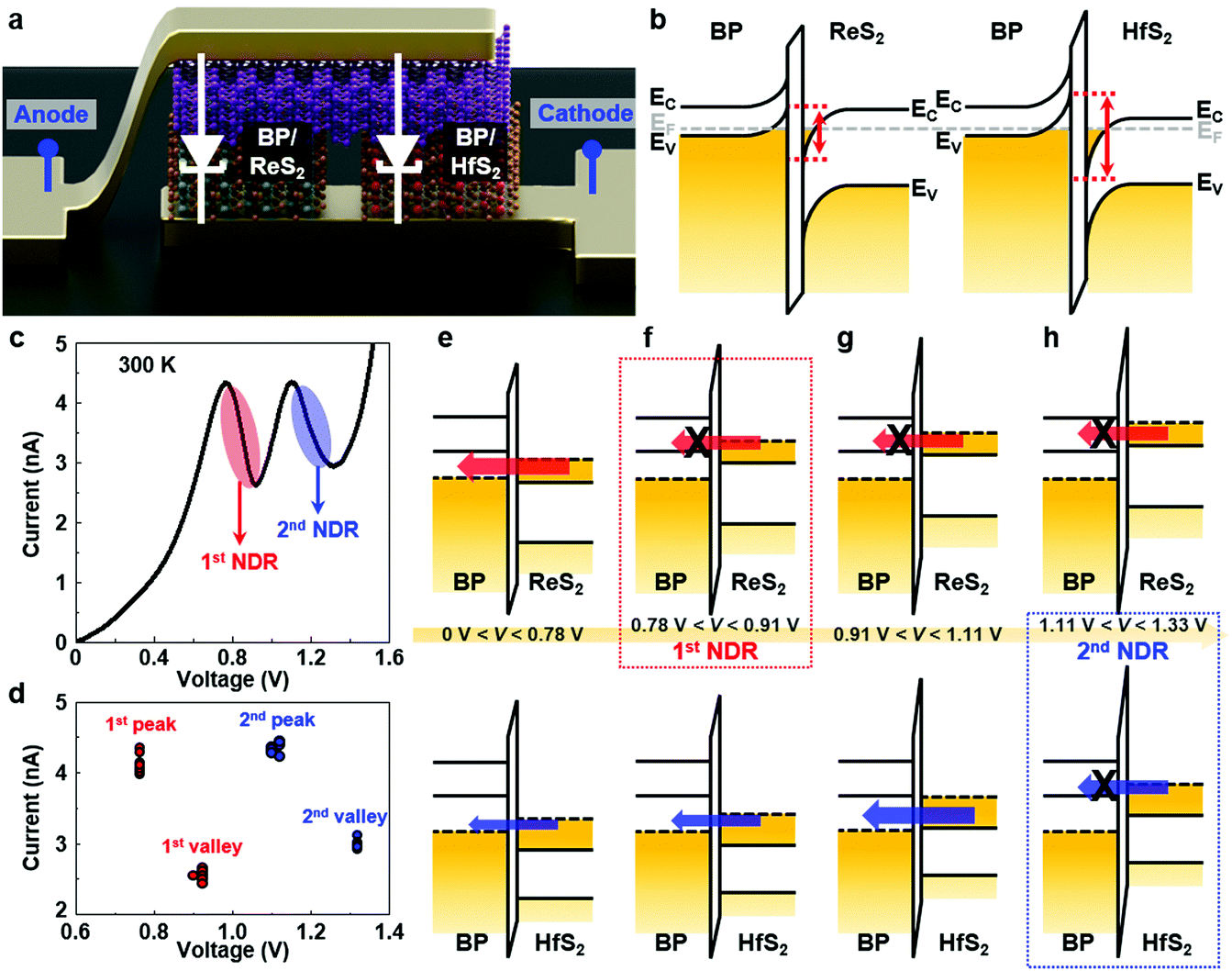 | ||
| Fig. 2 Electrical characteristics of the type-III double heterojunction device. (a) Schematic of the vertical tunneling device based on the BP/(ReS2 + HfS2) type-III double heterojunction. (b) Energy band structure of BP/ReS2 (left) and BP/HfS2 (right) heterojunctions under thermal equilibrium state. (c) The I–V characteristic of the BP/(ReS2 + HfS2) double heterojunction device. (d) The voltage and current values extracted at the peak and valley current positions (1st: red and 2nd: blue), which were obtained for 10-times consecutive I–V sweeps. (e–h) Energy band alignment of BP/ReS2 (top row) and BP/HfS2 (bottom row) heterojunction devices under various voltage biases. The size of the red arrows describes the magnitude of the current. | ||
We also evaluated the effect of a broken energy gap on the I–V characteristics of the NDR tunneling devices in detail. For this purpose, we prepared two types of heterojunctions: BP/ReS2 and BP/HfS2, as shown in Fig. 3a. Fig. 3b shows the I–V characteristics of the NDR devices formed on the individual BP/ReS2 (red) and BP/HfS2 (blue) junctions, where the black curve corresponds to the case where these two devices were connected in parallel. The peak current of the BP/ReS2 device occurred at 0.78 V (red), and that of the BP/HfS2 device was seen at the point moved by 0.3 V (1.08 V, blue) owing to the larger broken energy gap. The electrical data measured in additional devices for checking the reliability are presented in Fig. S7 (ESI†). The peak current profile of the BP/HfS2 device was slightly wider than that of the BP/ReS2 device. This can be quantitatively explained by the full width at half maximum (FWHM), which is defined as the difference between two voltage points at 50% of the peak current. The FWHM obtained in the BP/HfS2 device was approximately 0.46 V, which was larger than that in the BP/ReS2 device (approximately 0.3 V). This difference originated from the difference in the broken energy gap between the two type-III heterojunctions. As the broken energy gap increased, a larger voltage bias was needed to reach the peak and valley currents, increasing the FWHM. The correlation between the broken energy gap and the I–V characteristic was theoretically verified using the I–V curves predicted by our analytical NDR device model constituting tunneling and diffusion current equations (the current equations and parameters are presented in the Experimental section and Table S3, ESI†). To investigate the effect of the broken gap on the NDR characteristic curve, the device was modelled under the ideal assumption that there were no interface trap states at the heterojunction (the effect of interface states on the NDR characteristic curve was additionally discussed in Fig. S16, ESI†). Fig. 3c shows the calculated I–V curves for various broken energy gaps. As the broken energy gap increased from 0.1 to 0.4 eV, the peak current shifted by 0.26 V in the positive voltage direction, and the FWHM increased by 0.24 V (Fig. 3d). This dependence on the broken gap is consistent with that observed in the aforementioned experimental results. However, in the calculated I–V characteristic curves, the tunneling current gradually increased as the broken gap increased. This discrepancy between the experimental and theoretical I–V data likely resulted from the barrier-height difference between the Au/ReS2 and Au/HfS2 junctions, which was not considered in the I–V analytical model. To support this claim, we extracted the Schottky barrier heights at the BP/ReS2 and BP/HfS2 junctions, as shown in Fig. 3e. The barrier height at Au/HfS2 (210 meV) was approximately 12 times larger than that at Au/ReS2 (18 meV); thus, a significantly lower electron injection rate was expected at the Au/HfS2 contact junction (Fig. 3f). This eventually appeared to reduce the tunneling current through the BP/HfS2 heterojunction path, in contrast to the theoretical prediction. Furthermore, the channel resistance determined by the HfS2 thickness might affect the tunneling current slightly, which is expected to cause subtle variations of m-NDR characteristics, such as the position of the peak current, the difference in the 1st and the 2nd peak positions, and the peak-to-valley ratio (PVCR) (Fig. S8 and S12, ESI†). We additionally provide strategies for adjusting this m-NDR characteristic in Fig. S14 (ESI†).
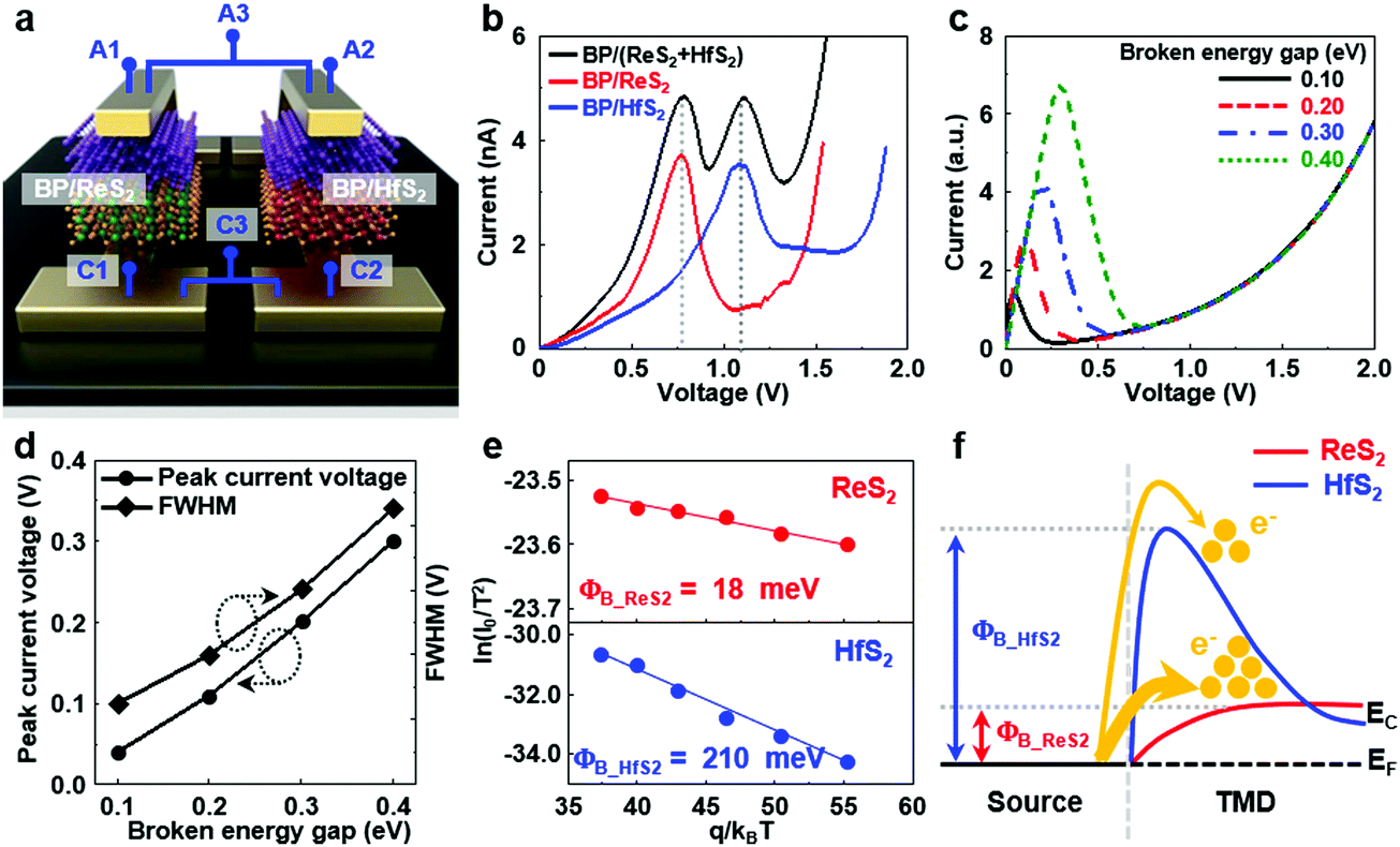 | ||
| Fig. 3 Analysis of electrical characteristics in individual BP/ReS2 and BP/HfS2 heterojunction devices. (a) Schematic of the heterojunction devices used for the analysis. (b) I–V characteristics of BP/ReS2 (red), BP/HfS2 (blue), and their parallel-connected type-III heterojunction devices (black). (c) Theoretically calculated I–V characteristics of a type-III heterojunction depending on the broken energy gap. (d) Peak current voltage and full width at half maximum (FWHM) as a function of the broken energy gap. (e) Arrhenius plot for extraction of Schottky barrier heights at the Au/ReS2 (top) and Au/HfS2 (bottom) junctions. (f) Schematic explaining the electron injection at the Au/ReS2 and Au/HfS2 junctions. | ||
Finally, we demonstrated a ternary latch circuit consisting of a BP/(ReS2 + HfS2) double-NDR tunneling device and an h-BN/WSe2 p-channel thin-film transistor (TFT), as schematically shown in Fig. 4a. Compared with the latch in the conventional binary 6T SRAM, which consists of two interlocked CMOS inverters (i.e., four transistors), the proposed ternary latch circuit can store one additional state (a total of three states) with less components (only two devices). Fig. 4b and c present an optical image and the circuit configuration of the ternary latch, respectively. The p-channel TFT serving as a load was connected to the anode of the tunneling device. The source of the h-BN/WSe2 TFT was connected to the supply voltage (VDD), and the cathode of the tunneling device was grounded. The output voltage (VOUT) was measured at the storage node (SN) shared by the BP/(ReS2 + HfS2) tunneling device and the h-BN/WSe2 TFT. By supplying appropriate voltage biases (VDD = 1.7 V and VSG = 2 V) to the p-channel TFT, the blue dashed load line was configured to intersect the positive differential resistance regions, providing three stable operating points: V1, V2, and V3 (Fig. 4d). The load line also intersected with the NDR regions, but the resulting operating points were metastable and vulnerable to extremely small noises. Owing to the self-latching operation of the circuit, the operating points V1–V3 were stable and acted as ternary states of the latch. For example, if the initially stored VOUT was V1 and VOUT became V1 + α or V1–α owing to the voltage noise of α or −α, the parasitic capacitor at the SN (CSN) was discharged or charged by the restoring current, and VOUT returned to V1 (refer to Fig. S9, ESI†). Fig. 4e shows the input signal waveforms (black dashed line) and the corresponding output voltage (red solid line) of the ternary latch circuit. We applied an input square pulse with an amplitude of 0.7 V to the SN, which was close to the voltage value of the V1 state. The square pulse charged CSN to 0.7 V, and then the voltage across the tunneling device settled to the stable operating point V1 after the input pulse ended, eventually entering the first of the three states. Similarly, we confirmed the existence of two other stable states (V2 and V3) at the output node. The performance of the ternary latch circuit will be improved further if the PVCR of the m-NDR device can be increased in future work (Fig. S13, ESI†). In addition, the ternary latch circuit can be extended to more than a quaternary, if more than two NDR characteristic curves are achieved in one NDR device. The possibilities and challenges on increasing the number of NDR curves are described in Fig. S15 (ESI†).
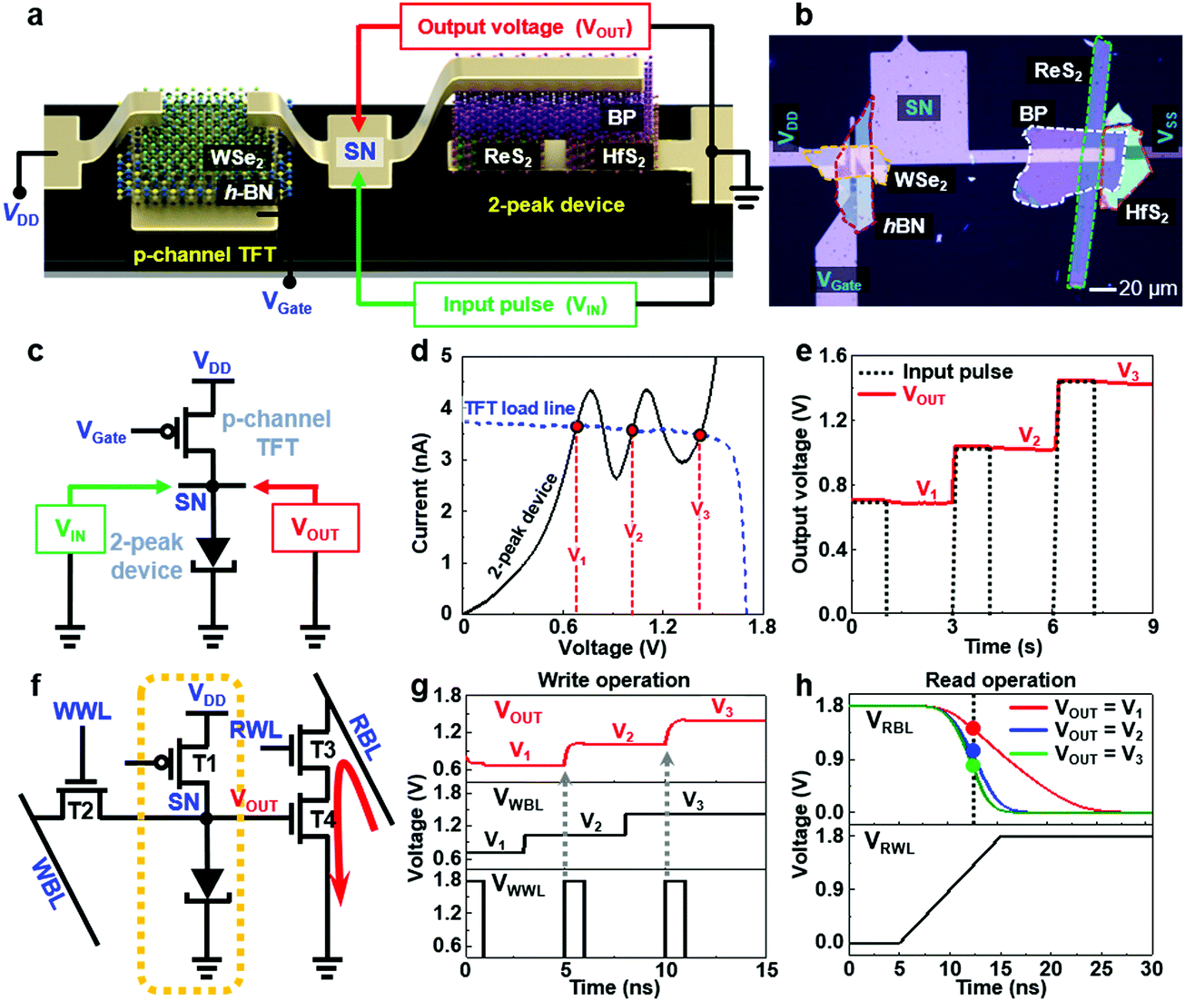 | ||
| Fig. 4 Ternary latch and static random access memory (SRAM). (a) Schematic illustration of the ternary latch. (b) Optical image of the ternary latch. (c) Equivalent circuit configuration of the ternary latch. (d) Load-line configuration of the ternary latch circuit exhibiting three stable operating points (V1, V2 and V3). (e) VINversus VOUT characteristic of the ternary latch. (f) Circuit configuration of ternary SRAM. WWL, WBL, RWL and RBL denote write word line, write bit line, read word line and read bit line, respectively. (g) Write operation of ternary SRAM. (h) Read operations of the ternary SRAM. | ||
Although the ternary latch circuit successfully showed a storage operation, for extension toward ternary SRAM, write and read operations should also be verified. For this purpose, we theoretically configured a ternary SRAM circuit with the ternary latch and a few transistors and then analyzed the circuit with regard to the write and read operations. Fig. 4f shows the designed ternary SRAM circuit, in which we used a device component driven by the double-NDR I–V characteristic data (Fig. S10, ESI†). The other parts of the circuit were designed by using transistors (T1, T2, T3, and T4) provided by the TSMC 180 nm process design kit (PDK) library (the detailed transistor specifications are presented in Table S4, ESI†). By simulating the ternary SRAM circuit, its write and read operations were verified, as shown in Fig. 4g and h, respectively. If the write access transistor T2 turns on (VWWL = VDD), the write-bit-line data (VWBL is driven to V1, V2, or V3) are transferred to the storage node (VOUT = VWBL) because the parasitic capacitor at the storage node is charged or discharged by the drain current of T2. Therefore, the states such as V1, V2, and V3 can be written and stored in the ternary SRAM. In particular, to minimize the write delay in the charging or discharging process, we used a transistor with a high driving current (approximately, 200 μA μm−1) as the access transistor. We consequently reduced the width of the VWWL pulse to 1 ns, which is very close to that of the voltage pulse operating a conventional 6T SRAM.47 Additionally, as shown in Fig. 4h, this circuit properly reads the different voltage states stored in the ternary latch circuit. This read operation is based on the method to distinguish the voltage of the read-bit-line capacitor (CRBL), which is VRBL, at a specific time (black dotted line) when the CRBL is partially discharged by T3 and T4. This is because the restoring current of this ternary latch is <1 nA, and it would take a long time to directly charge or discharge the large CRBL (usually, CRBL ≫ CSN). Thus, to achieve high-speed read operation, we chose the strategy of using the stored voltages to induce the discharging current (red arrow in Fig. 4f) at the T4 transistor. Because the stored voltages are always lower than VRWL (= VDD if T3 turns on), the discharging current is mainly controlled by the T4 transistor. The discharging speed differs according to the three stored voltage states; the voltage of CRBL can be distinguished, as indicated by the red, blue, and green dots, especially within 7 ns. This is because 50 mV or less difference in the output voltage can be distinguished by the operational amplifier that will be connected to the read bit-line. This speed of read access is comparable to that of conventional 6T SRAM.47
Conclusions
In conclusion, we demonstrated the m-NDR phenomenon in a single vdW tunneling device formed on a BP/(ReS2 + HfS2) type-III double-heterojunction structure. This m-NDR phenomenon was achieved by the principle that the tunneling currents through the BP/ReS2 and BP/HfS2 junctions are blocked by the BP bandgap at different bias points. This is because the BP/ReS2 and BP/HfS2 junctions have different broken energy gaps at 0.08 and 0.42 eV, respectively. These gap values were experimentally obtained through μ-XPS-based CL spectra analysis performed on the 2D crystal materials. On the determined band structure, we then explained the operating mechanism of the vdW tunneling device by considering the tunneling and diffusion phenomena. To obtain a detailed understanding of the relationship between the broken energy gap and the NDR I–V characteristic, we also performed I–V measurements on the individual BP/ReS2 and BP/HfS2 devices. We consequently confirmed that the position and FWHM of the peak current of the devices exhibited differences of 0.3 and 0.16 V, respectively, owing to the difference in the broken energy gap. The correlation between the broken energy gap and the NDR I–V characteristic was verified again using our analytical NDR device model. When the broken energy gap was changed from 0.1 to 0.4 eV, the peak current position and FWHM of the NDR device model changed by 0.26 and 0.24 V, respectively. Finally, we experimentally demonstrated a ternary latch circuit capable of storing three logic states by connecting the vdW double-NDR device and the p-channel vdW transistor in series. The three logic states were confirmed to be stably maintained through the self-latching operation of the circuit. This ternary latch circuit was theoretically extended toward ternary SRAM, and its operation for writing and reading the logic states was verified. By properly designing the write and read circuit parts, high-speed operation where write and read access was performed at the levels of 1 and 7 ns, respectively, was achieved, which is comparable to the operating speed of conventional 6T SRAM.Experimental
Fabrication of BP/(ReS2 + HfS2) double-heterojunction vertical tunneling devices
A 10 μm-wide cathode region was defined on a 90 nm-thick SiO2/Si substrate using a photolithography process, followed by Ti/Au (5/10 nm) deposition using an electron-beam evaporator. Then, BP, ReS2, and HfS2 flakes were mechanically transferred onto the cathode to form the double heterojunction (Fig. S1, ESI†). Finally, a 10 μm-wide anode was formed via photolithography and Ti/Au (10/40 nm) deposition processes.Implementation and characterization of the ternary latch circuit
First, the BP, ReS2, and HfS2 flakes were transferred onto the cathode (Ti/Au, 5/10 nm) of the tunneling device. The anode region for the tunneling device and all electrode (source, drain, and gate) regions for the load transistor were simultaneously patterned using a photolithography process, followed by Ti/Au (10/40 nm) deposition using an electron-beam evaporating system. To form the gate oxide and the channel of the load transistor, an h-BN flake was transferred onto the gate electrode, and then a WSe2 flake was precisely transferred on top of the h-BN flake to connect the source and drain electrodes (see the optical image of the ternary latch circuit in Fig. 4c). The VDD was supplied to the source electrode of the h-BN/WSe2 TFT, and the cathode of the BP/(ReS2 + HfS2) tunneling device was connected to the ground (VSS). In order to configure the tri-state load line, we obtained the desired drain current in the h-BN/WSe2 transistor by adjusting its gate voltage. Input pulses generated by pulse generator (Keysight 33500B) were then applied to the SN node, and the output voltage stored at the SN node was measured using an electrometer with tera-Ohm output impedance (Keithley 6517b).Characterization of the BP/(ReS2 + HfS2) double heterojunction
For the structural analysis of the BP/(ReS2 + HfS2) double heterojunction, a high-resolution TEM measurement was conducted using a JEM-2100F. The atomic composition in the junction region was confirmed through EDS measurements using an Oxford X-Max 80TLE. To investigate the CLs of the vdW materials used in this study, XPS was performed using a PHI Quantera II (X-ray beam with a spot size of 10 μm and power of 15 keV). The electrical measurements of the double-heterojunction device were performed at room temperature under ambient conditions using a probe station with a Keysight B2912A.Theoretical carrier-transport model for a vdW tunneling device formed on the BP/MS2 heterojunction
To understand the carrier transport in the vdW tunneling devices in detail, we developed an analytical device model incorporating the tunneling (Itunnel) and diffusion (Idiff) current equations. The total current (Itotal) of the vdW tunneling device is the sum of these two currents, as follows:| Itotal = Itunnel + Idiff |
where q is the elementary charge, h is Planck's constant, EV_BP is the valence band maximum energy in BP, α is the fitting parameter, EC_MS2 is the conduction band minimum energy in MS2 (M represents a transition metal such as Re or Hf), and V is the applied voltage. DOSBP(E) and DOSMS2(E) represent the density of states of BP and MS2, respectively, and fBP(E) and fMS2(E) represent the density of states and the Fermi–Dirac distribution functions of BP and MS2, respectively. Detailed information regarding the parameters used in the vdW tunneling device model is presented in Table S4 (ESI†). The second equation for Idiff is given as

where I0 is the saturation current, n is the ideality factor, kB is the Boltzmann constant, and T is the temperature.

Conflicts of interest
There are no conflicts to declare.Acknowledgements
This work was supported by Samsung Research Funding & Incubation Center of Samsung Electronics under Project Number SRFC-MA1701-02.Notes and references
- R. Ho, K. W. Mai and M. A. Horowitz, The future of wires, Proc. IEEE, 2001, 89, 490–504 CrossRef.
- P. Apte, T. Salmon, R. Rice, M. Gerber, R. Beica, J. Calvert, D. Hemker, Y. Dordi, M. Ranjan, S. Ramalingam, J. Gandhi, A. Kaviani, S. Mitra, P. Wong, V. Lee and M. El-Sabry, Future Interconnect Materials and System Integration Strategies for Data-Intensive Applications, 7th Electronics System-Integration Technology Conference, 2018, p. 1.
- M. Huang, S. Li, Z. Zhang, X. Xiong, X. Li and Y. Wu, Multifunctional high-performance van der Waals heterostructures, Nat. Nanotechnol., 2017, 12, 1148–1154 CrossRef CAS PubMed.
- J. Shim, S. Oh, D.-H. Kang, S.-H. Jo, M. H. Ali, W.-Y. Choi, K. Heo, J. Jeon, S. Lee, M. Kim, Y. J. Song and J.-H. Park, Phosphorene/rhenium disulfide heterojunction-based negative differential resistance device for multi-valued logic, Nat. Commun., 2016, 7, 13413 CrossRef CAS PubMed.
- L. Britnell, R. V. Gorbachev, A. K. Geim, L. A. Ponomarenko, A. Mishchenko, M. T. Greenaway, T. M. Fromhold, K. S. Novoselov and L. Eaves, Resonant tunneling and negative differential conductance in graphene transistors, Nat. Commun., 2013, 4, 1794 CrossRef CAS PubMed.
- A. Mishchenko, J. S. Tu, Y. Cao, R. V. Gorbachev, J. R. Wallbank, M. T. Greenaway, V. E. Morozov, S. V. Morozov, M. J. Zhu, S. L. Wong, F. Withers, C. R. Woods, Y.-J. Kim, K. Watanabe, T. Taniguchi, E. E. Vdowin, O. Makarovsky, T. M. Formhold, V. I. Fal’ko, A. K. Geim, L. Eaves and K. S. Novoelov, Twist-controlled resonant tunneling in graphene/boron nitride/graphene heterostructures, Nat. Nanotechnol., 2014, 9, 808–813 CrossRef CAS PubMed.
- Y.-C. Lin, R. K. Ghosh, R. Addou, N. Lu, S. M. Eichfeld, H. Zhu, M.-Y. Li, X. Peng, M. J. Kim, L.-J. Li, R. M. Wallace, S. J. Datta and A. Robinson, Atomically thin resonant tunnel diodes built from synthetic van der Waals heterostructures, Nat. Commun., 2015, 6, 7311 CrossRef CAS PubMed.
- M. L. Perrin, R. Frisenda, M. Koole, J. S. Seldenthuis, J. A. Celis Gill, H. Valkenier, J. C. Hummelen, N. Renaud, F. C. Grozema, J. M. Thijssen, D. Dulic and H. S. J. van der Zant, Large negative differential conductance in single-molecule break junctions, Nat. Nanotechnol., 2014, 9, 830–834 CrossRef CAS PubMed.
- W. S. Choi, S. A. Lee, J. H. You, S. Lee and H. N. Lee, Resonant tunneling in a quantum oxide superlattice, Nat. Commun., 2015, 6, 7424 CrossRef CAS PubMed.
- D. Sarkar, X. Xie, W. Liu, W. Cao, J. Kang, Y. Gong, S. Kraemer, P. M. Ajayan and K. Banerjee, A subthermionic tunnel field-effect transistor with an atomically thin channel, Nature, 2015, 526, 91–95 CrossRef CAS PubMed.
- J. Shim, S.-H. Bae, W. Kong, D. Lee, K. Qiao, D. Nezich, Y. J. Park, R. Zhao, S. Sundaram, X. Li, H. Yeon, C. Choi, H. Kum, R. Yue, G. Zhou, Y. Ou, K. Lee, J. Moodera, X. Zhao, J.-H. Ahn, C. Hinkle, A. Ougazzaden and J. Kim, Science, 2018, 362, 665–670 CrossRef CAS PubMed.
- K. Kobashi, R. Hayakawa, T. Chikyow and Y. Wakayama, Multi-Valued Logic Circuits Based on Organic Anti-ambipolary Transistors, Nano Lett., 2018, 18, 4355–4359 CrossRef CAS PubMed.
- A. Nourbakhsh, A. Zubair, M. S. Dresselhaus and T. Palacios, Transport Properties of a MoS2/WSe2 Heterojunction Transistor and Its Potential for Application, Nano Lett., 2016, 16, 1359–1366 CrossRef CAS PubMed.
- J. Shim, S.-H. Jo, M. Kim, Y. J. Song, J. Kim and J.-H. Park, Ligh-Triggered Ternary Device and Inverter Based on Heterojunction of van der Waals Materials, ACS Nano, 2017, 11, 6319–6327 CrossRef CAS PubMed.
- R. Yan, S. Fathipour, Y. Han, B. Song, S. Xiao, M. Li, N. Ma, V. Protasenko, D. A. Muller, D. Jena and H. G. Xing, Esaki Diodes in van der Waals Heterojunctions with Broken-Gap Energy Band Alignment, Nano Lett., 2015, 15, 5791–5798 CrossRef CAS PubMed.
- K. Kim, N. Prasad, H. C. P. Movva, G. W. Burg, Y. Wang, S. Larentis, T. Taniguchi, K. Watanabe, L. F. Register and E. Tutuc, Edge-Limited Valley-Preserved Transport in Quasi-1D Constriction of Bilayer Graphene, Nano Lett., 2018, 18, 5961–5966 CrossRef PubMed.
- G. C. Constantinescu and N. D. M. Hine, Multipurpose Black-Phosphorus/hBN Heterostructures, Nano Lett., 2016, 16, 2586–2594 CrossRef CAS PubMed.
- G. W. Burg, N. Prasad, B. Fallahazad, A. Valsaraj, K. Kim, T. Taniguchi, K. Watanabe, Q. Wang, M. J. Kim, L. F. Register and E. Tutuc, Coherent Interlayer Tunneling and Negative Differential Resistance with High Current Density in Double Bialyer Graphene-WSe2 Heterostructures, Nano Lett., 2017, 17, 3919–3925 CrossRef CAS PubMed.
- T. Roy, M. Tosun, X. Cao, H. Fang, D.-H. Lien, P. Zhao, Y.-Z. Chen, Y.-L. Chueh, J. Guo and A. Javey, Dual-Gated MoS2/WSe2 van der Waals Tunnel Diodes and Transistors, ACS Nano, 2015, 9, 2071–2079 CrossRef CAS PubMed.
- P. M. Campbell, A. Tarasov, C. A. Joiner, W. J. Ready and E. M. Vogel, Enhanced Resonant Tunnerling in Symmetric 2D Semiconductor Vertical Heterostructgure Transistors, ACS Nano, 2015, 9, 5000–5008 CrossRef CAS PubMed.
- P. M. Campbell, A. Tarasov, C. J. Joiner, W. J. Ready and E. M. Vogel, Band structure effects on resonant tunneling in III-V quantum wells versus two-dimantional vertical heterostructures, J. Appl. Phys., 2016, 119, 024503 CrossRef.
- G. W. Burg, B. Fallahazad, K. Kim, N. Prasad, T. Taniguchi, K. Watanabe, L. F. Register and E. Tutuc, Double bilayer graphene-WSe2 resonant tunneling heterostructures with high interlayer current densities and peak-to-vally ratios, 75th Annual Device Research Conference, 2017.
- O. B. Mohammed, H. C. P. Movva, N. Prasad, A. Valsaraj, S. Kang, C. M. Corbet, T. Taniguchi, K. Watanabe, L. F. Register, E. Tutuc and S. K. Banerjee, ReS2-based interlayer tunnel field effect transistor, J. Appl. Phys., 2017, 122, 245701 CrossRef.
- X. Liu, D. Qu, M. S. Choi, C. Lee, H. Kim and W. J. Yoo, Appl. Phys. Lett., 2018, 112, 183103 CrossRef.
- X. Liu, D. Qu, H.-M. Li, I. Moon, F. Ahmed, C. Kim, M. Lee, Y. Choi, J. H. Cho, J. C. Hone and W. J. Yoo, Modulation of Quantum Tunneling via a Vertical Two-Dimantional Black Phosphorus and Molybdenum Disulfide p-n Junction, ACS Nano, 2017, 11, 9143–9150 CrossRef CAS PubMed.
- T. Roy, M. Tosun, M. Hettick, G. H. Ahn, C. Hu and A. Javey, 2D-2D tunneling field-effect transistors using WSe2/SnSe2 heterostructures, Appl. Phys. Lett., 2016, 108, 083111 CrossRef.
- B. Fallahazad, K. Lee, S. Kang, J. Xue, S. Larentis, C. Corbet, K. Kim, H. C. P. Movva, T. Taniguchi, K. Watanabe, L. F. Register, S. K. Banerjee and E. Tutuc, Gate-Tuanble Resonant Tunneling in Double Bilayer Graphene Heterostructures, Nano Lett., 2015, 15, 428–433 CrossRef CAS PubMed.
- W. Dickerson, V. Tayari, I. Fakih, A. Korinek, M. Caporali, M. Serrano-Ruiz, M. Peruzzini, S. Heun, G. A. Botton and T. Szkopek, Phosphorus oxide gate dielectric for black phosphorus field effect transistors, Appl. Phys. Lett., 2018, 112, 173101 CrossRef.
- L. Esaki, New Phenomenon in Narrow Germanium p-n Junctions, Phys. Rev., 1958, 109, 603 CrossRef CAS.
- J. P. A. van der Wagt, Tunneling-based SRAM, Nanotechnology, 1999, 10, 174 CrossRef CAS.
- H. Tang and H. Lin, Multi-valued decoder based on resonant tunneling diodes in current tapping mode, Proc. 26th Int. Symp. Multiple-Valued Logic, 1996, p. 230.
- T. Waho, K. J. Chen and M. Yamamoto, Resonant-tunneling diode and HEMT logic circuits with multiple thresholds and multilevel output, IEEE J. Solid-State Circuits, 1998, 33, 268–274 CrossRef.
- P. Mazumder, S. Kulkarni, M. Bhattacharya, J. P. Sun and G. I. Haddad, Digital circuit applications of resonant tunneling devices, Proc. IEEE, 1998, 86, 664–686 CrossRef.
- E. Ozer, R. Sendag and D. Gregg, Multiple-Valued Logic Buses for Reducing Bus Zide, Transitions and Power in Deep Submicron Technologies. Advanced Networking and Communications Hardware Workshop, 2005 Search PubMed.
- E. Ozer, R. Sendag and D. Gregg, Multiple-valued logic buses for recuging bus energy in low-power systems, IEE Proc. Comput. Digit. Technol., 2006, 153, 270–282 CrossRef.
- S. P. Kowalczyk, J. T. Cheung, E. A. Kraut and R. W. Grant, CdTe-HgTe Heterojunction Valence-Band Discontinuity: A Common-Anion-Rule Contradiction, Phys. Rev. Lett., 1986, 56, 1605 CrossRef CAS PubMed.
- M. Tangi, P. Mishra, T. K. Ng, M. N. Hedhili, B. Janjua, M. S. Alias, D. H. Anjum, C.-C. Tseng, Y. Shi, H. J. Joyce, L.-J. Li and B. S. Ooi, Determination of band offsets at GaN/single-layer MoS2 heterojunction, Appl. Phys. Lett., 2016, 109, 032104 CrossRef.
- S. Kundu, M. Clavel, P. Biswas, B. Chen, H.-C. Song, P. Kumar, N. N. Halder, M. K. Hudait, P. Banerji, M. Sanghadasa and S. Priya, Lead-free epitaxial ferroelectric material integration on semiconducting (100) Nb-doped SrTiO3 for low-power non-volatile memory and efficient ultraviolet raty detection, Sci. Rep., 2015, 5, 12415 CrossRef PubMed.
- J. R. Waldrop, S. P. Kowalczyk, R. W. Grant, E. A. Kraut and D. L. Miller, XPS measurement of GaAs-AlAs heterojunction band discontinuities: Growth sequence dependence, J. Vac. Sci. Technol., 1981, 9, 573 CrossRef.
- S. McDonnell, A. Azcatl, R. Addou, C. Gong, C. Battaglia, S. Chuang, K. Cho, A. Javey and R. M. Wallace, Hole Contacts on Transition Metal Dichalcogenides: Interface Chemistry and Band Alignments, ACS Nano, 2014, 8, 6265–6272 CrossRef CAS PubMed.
- H. C. Diaz, R. Addou and M. Batzill, Interface properties of CVD grown graphene transferred onto MoS2(0001), Nanoscale, 2014, 6, 1071–1078 RSC.
- R. Schlaf, B. A. Parkinson, P. A. Lee, K. W. Nebesny and N. R. Armstrong, Determination of frontier orbital alignment and band bending at an organic semiconductor heterointerface by combined x-ray and ultraviolet photoemission measurements, Appl. Phys. Lett., 1998, 73, 1026 CrossRef CAS.
- X.-R. Nie, B.-Q. Sun, H. Zhu, M. Zhang, D.-H. Zhao, L. Chen, Q.-Q. Sun and D. W. Zhang, Impact of Metal Contacts on the Performance of multilayer HfS2 Field-Effect Transistors, ACS Appl. Mater. Interfaces, 2017, 9, 26996–27003 CrossRef CAS PubMed.
- C. Gong, H. Zhang, W. Wang, L. Colombo, R. M. Wallace and K. Cho, Band alignment of two-dimensional transition metal dichalcogenides: Application in tunnel field effect transistors, Appl. Phys. Lett., 2013, 103, 053513 CrossRef.
- C.-H. Ho, Y. S. Huang, J. L. Chen, T. E. Dann and K. K. Tiong, Electronic structure of ReS2 and ReSe2 from fisrt-principles calculations, photoelectron spectroscopy, and electrolyte electroreflectance, Phys. Rev. B: Condens. Matter Mater. Phys., 1999, 60, 15766 CrossRef CAS.
- D. J. Perello, S. H. Chae, S. Song and Y. H. Lee, High-performance n-type black phosphorus transistors with type control via thickness and contact-metal engineering, Nat. Commun., 2015, 6, 7809 CrossRef CAS PubMed.
- S. Yadav, N. Malik, A. Gupta and S. Rajput, Low Power SRAM Design with Reduced Read/Write Time, Int. J. Inf. Comput. Technol., 2013, 3, 195–200 Search PubMed.
- L. D. Landau and E. M. Lifshitz, Quantum Mechanics, Non-Relativistic Theory, Elsevier Science, 1958, vol. III Search PubMed.
- F. Wu, H. Xia, H. Sun, J. Zhang, F. Gong, Z. Wang, L. Chen, P. Wang, M. Long, X. We, J. Wang, W. Ren, X. Chen, W. Lu and W. Hu, AsP/InSe van der Waals Tunneling Heterojunctions with Ultrahigh Reverse Rectification Ratio and High Photosensitivity, Adv. Funct. Mater., 2019, 29, 12 Search PubMed.
- P. Paletti, R. Yue, C. Hinkle, S. K. Fullerton-Shirey and A. Seabaugh, Two-dimensional electric-double-layer Esaki diode, npj 2D Mater. Appl., 2019, 3, 19 CrossRef.
- T. Li, X. Li, M. Tian, Q. Hu, X. Wang, S. Li and Y. Wu, Negative transconductance and negative differenctial resistance in asymmetric narrow bandgap 2D-3D heterostructures, Nanoscale, 2019, 11, 4701–4706 RSC.
- S. Fan, Q. A. Vu, S. Lee, T. L. Phan, G. Han, Y.-M. Kim, W. J. Yu and Y. H. Lee, Tunable Negative Differential Resistance in van der Waals Heterostructures at Room Temperature by Tailoring the Interface, ACS Nano, 2019, 13, 8193–8201 CrossRef CAS PubMed.
- N. T. Duong, J. Lee, S. Bang, C. Park, S. C. Lim and M. S. Jeong, Modulating the Functions of MoS2/MoTe2 van der Waals Heterostructure via Thickness Variation, ACS Nano, 2019, 13, 4478–4485 CrossRef CAS PubMed.
- H. Yoo, S. On, S. B. Lee, K. Cho and J.-J. Kim, Negative Transconductance Heterojunction Organic Transistors and their Application to Full-Swing Ternary Circuits, Adv. Mater., 2019, 31, 1808265 CrossRef PubMed.
- L. Lee, J. Hwang, J. W. Jung, J. Kim, H.-I. Lee, S. Heo, M. Yoon, S. Choi, N. V. Long, J. Park, J. W. Jeong, J. Kim, K. R. Kim, D. H. Kim, S. Im, B. H. Lee, K. Cho and M. M. Sung, ZnO composite nanolayer with mobility edge quantization for multi-value logic transistors, Nat. Commun., 2019, 10, 1998 CrossRef PubMed.
- W. Lv, X. Fu, W. Lv, J. Cai, B. Zhang, Z. Wei, Z. Liu and Z. Zeng, Multistate Logic Inverter Based on Black Phosphorus/SnSeS Heterostructure, Adv. Electron. Mater., 2018, 5, 1 Search PubMed.
- M.-M. Miriam, L.-P. Guillermo, C.-G. Andres, G.-N. Cristina and G.-H. Julio, Environmental effects in mechanical properties of few-layer black phosphorus, 2D Mater., 2016, 3, 031007 CrossRef.
- W.-C. Liu, J.-H. Tsai, W.-S. Lour, L.-W. Laih and C.-Z. Wu, Multiple Negative-Differential-Resistance (NDR) of InGaP/GaAs Heterostructure-Emitter Bipolar Transistor (HEBT), IEEE Electron Device Lett., 1996, 17(3), 130–132 Search PubMed.
Footnotes |
| † Electronic supplementary information (ESI) available. See DOI: 10.1039/c9nh00631a |
| ‡ These authors contributed equally to this work. |
| This journal is © The Royal Society of Chemistry 2020 |