
 Open Access Article
 This Open Access Article is licensed under a Creative Commons Attribution-Non Commercial 3.0 Unported Licence
Morphology and mechanical behavior of diamond films fabricated by IH-MPCVD
Rong Tu a,
Tiantian Xua,
Dengfeng Lia,
Song Zhang*a,
Meijun Yanga,
Qizhong Lib,
Lianmeng Zhanga,
Toshihiro Shimadaac,
Takashi Gotoad and
Ji Shiae
a,
Tiantian Xua,
Dengfeng Lia,
Song Zhang*a,
Meijun Yanga,
Qizhong Lib,
Lianmeng Zhanga,
Toshihiro Shimadaac,
Takashi Gotoad and
Ji Shiae
aState Key Laboratory of Advanced Technology for Materials Synthesis and Processing, Wuhan University of Technology, 122 Luoshi Road, Wuhan 430070, People's Republic of China. E-mail: kobe@whut.edu.cn; superkobe0104@gmail.com
bHubei Key Laboratory Advanced Technology of Automobile Parts, Wuhan University of Technology, 122 Luoshi Road, Wuhan 430070, People's Republic of China
cDivision of Applied Chemistry, Hokkaido University, Sapporo 060-0808, Japan
dInstitute for Materials Research, Tohoku University, 2-1-1 Katahira, Aoba-ku, Sendai 980-8577, Japan
eJapan Department of Metallurgy and Ceramics Science, Tokyo Institute of Technology, Tokyo 152-8552, Japan
First published on 30th April 2018
Abstract
Morphology of diamond films has been controlled via intermediate frequency induction heated microwave plasma chemical vapor deposition (IH-MPCVD), which was transformed with various substrate temperatures (Tsub = 923–1123 K) and CH4/H2 ratios (ηc = 0.5–2 vol%). The coupling effects of Tsub and ηc on the structure of diamond films have been studied. At ηc = 0.5 vol%, the sp3/sp2 ratio of diamond films reached 98% at 1073 K, surface roughness (Rms) increased from 50 to 85 nm with increasing Tsub, the maximum hardness (Ha) reached 84 GPa at 973 K, and the maximum Young's modulus (E) reached 642 GPa at 1023 K. The residual stress (σ) was calculated as a function of Tsub and ηc. The quality factor (Q), combining microstructure and mechanical behavior, has been creatively defined to evaluate the quality of diamond films.
1. Introduction
Chemical vapor deposited (CVD) diamond covers a broad range of synthetic diamond materials with great variety of properties such as high hardness, high elastic modulus, chemical inertness, and low self-friction coefficient.1–4 CVD diamond can be broadly divided into two grades, i.e., microcrystalline diamond (MCD) and nanocrystalline diamond (NCD), with the crystallites in the micron size range and smaller than 500 nm, respectively.5 NCD films are highly desirable for the substrates of MEMS (Micro-Electro-Mechanical Systems) because the smaller grain size insures a smoother surface for the devices above comparing with MCD.6–8 However, the mechanical properties of NCD, such as hardness and elastic modulus, are lower than those of conventional MCD due to the presence of sp2 non-diamond species.9 Therefore, the smooth surface, good mechanical property and high sp3/sp2 ratio are usually difficult to obtain simultaneously, and it is hard to evaluate the quality of diamond-related materials only according to their individual properties. Here, we define quality factor (Q), combining microstructure and mechanical behavior to evaluate the deposits.Besides, substrate temperature (Tsub) plays an important role in growth process of diamond. Not only the structure and properties of CVD diamond films, but also the growth rate is mainly influenced by Tsub. For example, the commonly low Tsub may hinder the formation of strong chemical bonds between atoms, while the high temperature may enhance the graphite species.10 However, it is difficult to control precisely the Tsub in MPCVD system because the Tsub is attributed to several factors, e.g., discharging plasma density and substrate location, which is influenced strongly by the microwave power (pw). Moreover, Tsub would certainly decrease due to the heat exchange between the chamber and external environment. And it is hard to increase the decreased Tsub by adjusting pw due to its strong influence on Tsub. In general, Tsub is difficult to be precisely controlled only through the adjustment of pw, which resulting in the difficulty of researches on diamond structures.
In this study, an IH-MPCVD apparatus was developed to fabricate diamond films. The Tsub was compensated with an intermediate frequency induction heating system by self-adjusting the IH power (ph) according to the thermocouple that set under the substrate. The effects of CH4/H2 ratio and deposition temperature on the morphology, quality factor (Q) and deposition rate of the diamond films has been investigated, and the growth mechanism of these films was also proposed.
2. Experimental
Fig. 1 shows the experimental schematic of the home-made induction heated microwave plasma CVD (IH-MPCVD). The system consisted of a microwave generator network (MPS-15D, NISSIN, Tokyo, Japan, 2.45 GHz, 1.5 kW), a quartz tube chamber, an intermediate frequency induction heating device (S08-6093, Daiichi Kiden, Tokyo, Japan, 6 kHz, 12.5 kW), and a vacuum system. A hollow graphite cylinder heated by the induction heating device was set below the substrate holder as heating unit surrounded by a graphite felt. The substrate holder was supported by an alumina tube within a K-type thermocouple. The temperature signals of thermocouple were fed back to the IH-system. | ||
| Fig. 1 Schematic diagram of the IH-MPCVD system. | ||
Single-crystalline silicon 〈100〉 wafers with dimensions of 10.0 × 15.0 × 0.5 mm were used as substrates. To enhance nucleation, the Si substrates were scratched via ultrasonic bath in acetone with diamond powders (10–40 μm) for 1 hour. The scratched substrates were taken ultrasonic cleaning in deionized water, and then dried in a N2 flow.
The substrates were preheated at 873 K in 30 minutes after quartz chamber was evacuated to 10−1 Pa. The input gas flow rate of H2 (fh) was 400 sccm. The flow rate of CH4 (fc) was varied from 1 to 10 sccm. The total pressure (Ptot) and the microwave power (pw) were 4 kPa and 900 W, respectively. The induction heating power (ph) of the intermediate frequency induction heating device was self-adjusted from 0 to 12.5 kW, according to the substrate temperature assessed by thermocouple. Thus, the substrate temperatures (Tsub) were controlled in the range of 923–1123 K. The depositions for all samples were carried out for a total time of 3 h.
Phase identification of the films was obtained by Raman spectra (LabRAM HR Evolution; Horiba, Paris, France) with the excitation of a diode laser 532 nm in wavelength. Crystalline phases were examined by X-ray diffraction with Cu-Kα radiation (XRD; Ultima III, Rigaku, Tokyo, Japan, at 40 kV and 40 mA). A field-emission scanning electron microscope (SEM; Quanta-250, FEI, Houston, TX, at 20 kV) was used to observe the film thickness and microstructure. The surficial roughness was analyzed by atomic force microscopy (AFM; Multimode 8-HR, Bruker, Santa Barbara, USA). The hardness and young's modulus were analyzed by a MTS Nano-indenter (Agilent Technologies G200, California, USA).
3. Results and discussion
Fig. 2(a)–(e) shows the surficial morphology of diamond films grown at Tsub = 1073 K and various CH4/H2 ratio (ηc) ranging from 0.5 to 2.5 vol%. At ηc = 0.5%, the film consisted of regulated quadrate grains with average size of 0.36 μm [Fig. 2(a)]. At ηc = 1.0% and 1.5%, the films exhibited faceted columnar structure with average grain size of 0.34 μm and 0.44 μm, respectively [Fig. 2(b and c)]. At ηc = 2.0%, the grains were coated by nanoparticles [Fig. 2(d)]. By increasing ηc to 2.5%, the films showed dense spherical “cauliflower-like” morphology [Fig. 2(e)]. The cauliflower-like structures was also observed by Hemawan11 via AP-MPCVD. They explained that the formation of spherical and polygonal shapes in the atmospheric pressure MPCVD was due to surface diffusion and condensation from vapor phase.12 The cross-sectional view [Fig. 2(f–j)] revealed the film thickness reached the maximum at ηc = 1.5%.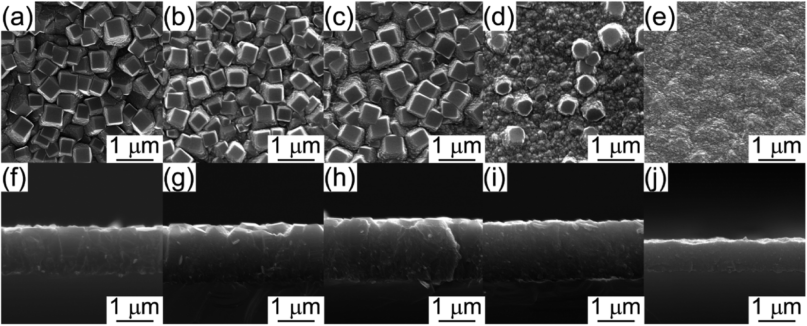 | ||
| Fig. 2 Surficial and cross-sectional SEM image of diamond films deposited at Tsub = 1073 K and various CH4/H2 ratio (ηc): (a and f) 0.5, (b and g) 1.0, (c and h) 1.5, (d and i) 2.0 and (e and j) 2.5 vol%. | ||
The minimum roughness (Rms) of film surface is approximately 23.4 nm at ηc = 2.0–2.5%, as shown in Fig. 3, which is much smaller than that obtained at low ηc = 1.0% (about 80 nm). Fig. 4 shows the XRD patterns of the deposit, the peaks corresponding to diamond (111) at 43.9° (2θ) were only detected for all the specimens, indicating (111) orientation. In terms of carbon chemistry in the plasma discharge, relatively higher ηc results in rich [CxHy] and other methyl radicals which are important for diamond nucleation. These species enhance the re-nucleation process of diamond, as well as the sp2 hybridized carbon formation.13 By reducing the CH4 fraction in the plasma, the CxHy species decreased, especially the species with x > 3 (e.g. [C4H2], [C3H2]). As a result, the hydrocarbon species with x ≤ 2 incorporates into the lattice by forming a C–C bond to an atom that belongs to a lower-lying terrace, and weaken the nucleation of sp2 hybridized carbon phase.5 Therefore, well-faceted diamond prefers relatively lower ηc under a constant microwave power in this study.
 | ||
| Fig. 3 Effect of ηc on the surface roughness and growth rate of the diamond films at Tsub = 1073 K. | ||
 | ||
| Fig. 4 XRD patterns of films deposited at Tsub = 1073 K and various ηc. | ||
Fig. 5 shows the cross-sectional and surficial SEM image of diamond films deposited at various Tsub ranging from 923 to 1123 K at ηc = 0.5%. The cross-sectional images revealed that the film thickness varied from 0.5 to 1.9 μm [Fig. 5(f)–(j)]. Namely, in this range, the substrate temperature caused an enhancement in diamond growth rate (RG).
 | ||
| Fig. 5 Cross-sectional and surficial SEM image of diamond films deposited at Tsub = 923 (a and f), 973 (b and g), 1023 (c and h), 1073 (d and i) and 1123 K (e and j) and ηc = 0.5 vol%. (k–n) is the Wulff configurations for diamond as a function of the facet growth ratio of {100} over {111}. | ||
The magnified details of the samples are given in Fig. 5(a)–(e), pyramidal micrometric diamond crystals are visible at the terminal surface, both triangular and square facets corresponding to {111} and {100} lattice plane were observed. The quadrate planes of {100} facets appear at all the samples [Fig. 5(a–e)], while the triangular {111} facets present at lower temperature [Fig. 5(a–c)]. Area ratio of square and triangular planes obviously grew larger with the increasing of Tsub (923–1073 K), owing to the different growth ratio (Rhkl) of each plane. According to the Wulff configurations,14 the slowest growing plane would be the one survive in growing diamond particles, and vice versa, the fastest one would disappear completely. Fig. 5(k–n) illustrate the Wulff configurations for diamond deposited at 923, 973, 1023, 1073 K respectively as a function of the facet growth ratio of {100} over {111}, defined as parameter α. The XRD result of this group sample shows that only diamond (111) at 43.9° (2θ) was detected, indicating (111) orientation.
Wild et al.15 introduced the growth parameter α which relates the growth rates along different crystal axes; 〈111〉 direction would be the fastest growing direction when α is 1, and the growth morphology would be cubic; when α is 3, the fastest growing direction would be 〈100〉 direction, and the growth morphology would be octahedron. For example, in addition to the twinning process, the CVD diamond would show truncated octahedron morphology in various scale when α is 1.5. In this study, for diamond deposited at 923–1023 K [Fig. 5(k)–(m)], α is 1 to 3, and α increase with Tsub. For diamond deposited at 1073 K [Fig. 5(n)], α is close to 3. In conclusion, the parameter α shows a negative relation with the rising Tsub, indicating that the R111 increases faster than the R100 with the Tsub [Fig. 5(a)–(d)].
Others have reported the order of calculated energy barriers of different diamond surface planes (i.e. {110} < {111} < {100}).16–19 Namely, {100} surface planes are the most stable facets of CVD diamond grains among H-rich plasma, and the hydrogen abstraction process on {111} facets run faster than those on {100} facets. The whole growth process of CVD diamond would speed up with increasing Tsub, as a result, the growth rate of 〈111〉 direction would be much faster than 〈100〉 direction.
Fig. 6 shows the surficial roughness increased with increasing Tsub except one grown at 1123 K and accompanied by an increasing of film thickness and grain size. These findings are understandable because the diamond film presents a columnar crystal cross-section in Fig. 5, which indicates that the evolution of grain size follows the van der Drift model14 with columnar structure. The diagram in Fig. 6 depicts the evolution of film thickness and surficial roughness in this temperature series.6,20,21 The surficial roughness and film thickness showed a positive correlation, except one grown at 1123 K. The AFM topographies suggest that the spherical carbon species may present at higher Tsub, and these amorphous little particles prefer to generate at the ravines between the micro-crystalline grains, which slightly decrease the roughness.
 | ||
| Fig. 6 Evolution of the surface roughness and growth rate of the diamond films synthesized at various Tsub, ηc = 0.5 vol%. | ||
Fig. 7 shows the dependence of the RG on the Tsub. The RG of diamond films, with a good quality, is at an intermediate level. The activation energy of 53 kJ mol−1 calculated by Arrhenius plot of the RG versus a reciprocal Tsub. The result indicates that diamond growth process is limited by temperature controlled chemical process, which under a constant microwave power. Stiegler et al.25 investigated the growth kinetics of diamond films deposited at low substrate temperatures (673–873 K), and they supposed that increasing RG is most probably caused by the removal of surface bonded hydrogen atoms from the carbon sites. Thus, we induced that with a higher temperature, the removal of surface bonded hydrogen atoms would get easier, and then caused a higher RG.
 | ||
| Fig. 7 Effect of Tsub on RG, ηc = 0.5 vol%. | ||
Fig. 8 indicates the Raman spectra for the films deposited at different Tsub. In all samples, a sharp peak has been observed at 1332 cm−1, which corresponds to the zone center of T2g symmetry of diamond. The other obvious characteristic peak occurs at 1575 cm−1 presenting the zone center E2g mode of crystalline graphite, and it is usually designated as the “G” band for graphite. Besides, in micro-crystalline graphite, an additional sharp peak should appear at a wave number of 1350 cm−1 in the Raman spectra, which represents a zone-edge A1g mode, named “D” band.27,28 However, the peak of “D” band, which close to the sharp diamond T2g peak, was absent from all the Raman spectra in Fig. 8. Namely, there is little crystalline graphite in these diamond films. In addition to the diamond and graphite, for all the other kinds of amorphous and nanocrystalline carbon species, the Raman spectra typically shows a shoulder and broad “G” band centered around 1550 cm−1 and a “D” band centered at 1375 cm−1.29 The intensity of sharp diamond peak is much higher than the other peaks, which indicates the higher proportion of sp3 carbon atoms in these samples. With increasing Tsub, the related intensity of broad G peak increases, and the “G” band slightly moves up to 1580 cm−1. The slight shift in the broad “G” band frequency is consistent with an increase of amorphous component which produced from the carbon soot formation.30 The downshift and broadening of the diamond peak in nanocrystalline diamond also have previously been observed and explained by quantum confinement effect.31 The phase purity is evaluated by the sp3/sp2 ratio (r) from the Raman spectra and expressed as eqn (1),32
 | (1) |
 is the sum of Raman sp2 phase peak areas. The factor 75 takes into account the more effective Raman scattering of sp2 structures.33,34 The sp3/sp2 ratio of samples shown in Fig. 8 are various from 93 to 98%. However, it should be noticed that two weak peaks occur at 1140 cm−1 and 1450 cm−1, respectively. Others have reported the two peaks not only appear together, yet they also show quite strong and similar dispersions, while the diamond mode does not. Moreover, Kuzmany et al.35 have given a clear proof that these peaks originate from trans-polyacetylene in the grain boundaries by the H–D isotopic substitution result. In Raman features observed here, these two peaks usually occur in the Raman spectra of samples deposited at low temperatures. This is due to the slow growth rate at low Tsub, and the re-nucleating process leads to a high nucleation density with a large amount of boundaries among little grains, where polyacetylene existed. In order to ensure the quality of diamond films, the Tsub during diamond growth process should not be higher than 1073 K, neither be lower than 973 K in this study.
 | ||
| Fig. 8 Raman spectra of the diamond films synthesized at various Tsub, ηc = 0.5 vol%. | ||
As shown in Fig. 9, the surficial morphologies of diamond films can be defined as three categories: the well-faceted crystalline, the spherical structures composited with nanoparticles, and the mixture of both morphologies. At a relative high Tsub (≥1073 K), {100} planes occurred on the film surface. For high CH4/H2 ratio (ηc ≥ 2.0%) and low Tsub (≤973 K), more spherical nanoparticles were formed instead of crystalline structure.
 | ||
| Fig. 9 Coupling effects of ηc and Tsub on structure of diamond films. | ||
In order to follow the mechanical properties, a nano-indentation technique was performed. Fig. 10 demonstrates the relationships between average hardness (Ha), Young's modulus (E) and Tsub. The Ha and E were calculated from the correlation between load/unload and displacement (i.e., displacement–load curves not shown here). The theoretical value of Poisson's coefficient (ν) used for calculating the Young's modulus was 0.20, according to the Poisson's ratio of CVD polycrystalline diamond.36 The results reveal that the Ha and E of films increased with Tsub when it ranged in 923–1073 K; the maximum Ha and E reached 84 GPa at 973 K and 642 GPa at 1023 K, respectively. The value is twice as much as regular NCD films by MPCVD,37 much hard than those deposited in argon plasma.38 Exceptionally, both Ha and E decreased marginally when Tsub beyond 1123 K. This anomaly may result from non-diamond phases generated among diamond crystals, confirmed by SEM, AFM and Raman spectra.
 | ||
| Fig. 10 Average hardness (Ha) and Young's modulus (E) of samples fabricated with various Tsub, ηc = 0.5 vol%. | ||
For most applications of diamond films, such as wear-resistant coatings, heatsinks, MEMS and surface acoustic wave devices, a high sp3 component, a high hardness and a low surface roughness are crucial and favorable, but are hard to possess simultaneously. For example, diamond film with an extreme smooth surface always shows a poor mechanical property and low sp3/sp2 ratio. To evaluate the quality of different diamond films by microstructure and mechanical behaviors, we proposed a parameter, quality factor (Q), as a formula model:
 | (2) |
Fig. 11 shows Q of DLC,39 NCD40 and diamond41 materials fabricated at different conditions (pw × ηc × Ptot), in which DLC, NCD and diamond area are classified by Q in the order of 1 × 10⁴, 1 × 10⁵ and 1 × 10⁶, respectively. Through comparing the values of Q, we could judge the quality of the diamond related materials more visually. Most specimens fabricated in this study are in the diamond area and NCD area, which demonstrates that with a relatively good quality, the diamond films in the present study would have a good performance in wear-resistant coatings, heatsinks, MEMS and surface acoustic wave devices.
 | ||
| Fig. 11 Quality factor (Q) of DLC, NCD and Diamond materials fabricated at different conditions (pw × ηc × Ptot). | ||
The residual stress (σ), as a function of various Tsub at ηc = 0.5% and various ηc at 1073 K was calculated by eqn (3).42
| σ = −0.567(ν − ν0) (GPa) | (3) |
 | ||
| Fig. 12 Residual stress variation with Tsub (ηc = 0.5%) and ηc (Tsub = 1073 K). | ||
4. Conclusions
To improve the thermal control process of MPCVD technique, we have explored an intermediate-frequency induction heated MPCVD (IH-MPCVD) system. Coupling effects of Tsub (923–1123 K) and ηc (0.5–2 vol%) on structure of diamond films shows that the surficial morphologies of diamond films can be defined as three categories: the well-faceted crystalline, the spherical structures composited with nanoparticles, and the mixture of both morphologies. Higher ηc (2.5 vol%) enhances the re-nucleation process which leads to a smooth surface, yet lower ηc (0.5 vol%) results in better crystalline quality of diamond films. At ηc = 0.5 vol%, the morphology transformed from pyramid to quadrate column with Tsub increasing from 923 to 1073 K, besides, the maximum hardness (Ha) and Young's modulus (E) was 84 GPa and 642 GPa, at Tsub = 1023, 1073 K, respectively. The residual stress increased from −1.54 to −0.79 GPa with Tsub, at ηc = 0.5 vol%, and then decreased, while at 1073 K, it increased with ηc and reached to 0.60 GPa at ηc = 2.5 vol%.Conflicts of interest
There are no conflicts to declare.Acknowledgements
This work was supported by the National Natural Science Foundation of China (No. 51372188, and 51521001) and by the 111 Project (B13035). This research was also supported by the International Science & Technology Cooperation Program of China (2014DFA53090) and the Natural Science Foundation of Hubei Province, China (2016CFA006), and the National Key Research and Development Program of China (2017YFB0310400), and the Fundamental Research Funds for the Central Universities (WUT: 2017II43GX, 2017III032, 2017YB004, 2018III016), and Science Challenge Project (No. TZ2016001).References
- F. A. Almeida, E. Salgueiredo, F. J. Oliveira, R. F. Silva, D. L. Baptista, S. B. Peripolli and C. A. Achete, ACS Appl. Mater. Interfaces, 2013, 5, 11725 CAS.
- J. J. Gracio, Q. H. Fan and J. C. Madaleno, J. Phys. D: Appl. Phys., 2010, 43, 374017 CrossRef.
- R. S. Balmer, J. R. Brandon, S. L. Clewes, H. K. Dhillon, J. M. Dodson, I. Friel, P. N. Inglis, T. D. Madgwick, M. L. Markham, T. P. Mollart, N. Perkins, G. a. Scarsbrook, D. J. Twitchen, a. J. Whitehead, J. J. Wilman and S. M. Woollard, J. Phys.: Condens. Matter, 2009, 21, 364221 CrossRef CAS PubMed.
- A. Gicquel, K. Hassouni, F. Silva and J. Achard, Curr. Appl. Phys., 2001, 1, 479 CrossRef.
- M. Eckert, E. Neyts and A. Bogaerts, Cryst. Growth Des., 2010, 10, 4123 CAS.
- S. H. Seo, W. C. Shin and J. S. Park, Thin Solid Films, 2002, 416, 190 CrossRef CAS.
- W. C. Shih, M. J. Wang and I. Nan Lin, Diamond Relat. Mater., 2008, 17, 390 CrossRef CAS.
- Y. Q. Fu, L. Garcia-Gancedo, H. F. Pang, S. Porro, Y. W. Gu, J. K. Luo, X. T. Zu, F. Placido, J. I. B. Wilson, A. J. Flewitt and W. I. Milne, Biomicrofluidics, 2012, 6, 024105 CrossRef CAS PubMed.
- S. A. Catledge, J. Borham, Y. K. Vohra, W. R. Lacefield, J. E. Lemons, S. A. Catledge, J. Borham and Y. K. Vohra, J. Appl. Phys., 2002, 91, 5347 CrossRef CAS.
- O. A. Williams, M. Daenen, J. D'Haen, K. Haenen, J. Maes, V. V Moshchalkov, M. Nesládek and D. M. Gruen, Diamond Relat. Mater., 2006, 15, 654 CrossRef CAS.
- K. W. Hemawan, H. Gou, R. J. Hemley, K. W. Hemawan, H. Gou and R. J. Hemley, Appl. Phys. Lett., 2015, 107, 181901 CrossRef.
- J. Kim, H. Sakakita, H. Ohsaki and M. Katsurai, Jpn. J. Appl. Phys., 2015, 54, 01AA02 CrossRef.
- H. J. Lee, K. S. Lee, J. M. Cho, T. S. Lee, I. Kim, D. S. Jeong and W. S. Lee, ACS Appl. Mater. Interfaces, 2013, 5, 11631 CAS.
- A. Van der Drift, Philips Res. Rep., 1967, 22, 267 CAS.
- C. Wild, R. Kohl, N. Herres, W. Müller-Sebert and P. Koidl, Diamond Relat. Mater., 1994, 3, 373 CrossRef CAS.
- J. Bühler and Y. Prior, J. Cryst. Growth, 2000, 209, 779 CrossRef.
- Y. Zou and K. Larsson, J. Phys. Chem. C, 2016, 120, 10658 CAS.
- K. E. Spear and J. P. Dismukes, in Synthetic Diamond, Wiley, New York, 1994, p. 663 Search PubMed.
- B. T. Van Regemorter and K. Larsson, Chem. Vap. Deposition, 2008, 224 CrossRef.
- R. Bogdanowicz, M. Sobaszek, J. Ryl, M. Gnyba, M. Ficek, Ł. Gołuński, W. J. Bock, M. Śmietana and K. Darowicki, Diamond Relat. Mater., 2015, 55, 52 CrossRef CAS.
- F. Bénédic, M. B. Assouar, F. Mohasseb, O. Elmazria, P. Alnot and A. Gicquel, Diamond Relat. Mater., 2004, 13, 347 CrossRef.
- S. Schwarz, S. M. Rosiwal, M. Frank, D. Breidt and R. F. Singer, Diamond Relat. Mater., 2002, 11, 589 CrossRef CAS.
- M. S. You, F. C. N. Hong, Y. R. Jeng and S. M. Huang, Diamond Relat. Mater., 2009, 18, 155 CrossRef CAS.
- M. J. Ulczynski, B. Wright and D. K. Reinhard, Diamond Relat. Mater., 1998, 7, 1639 CrossRef CAS.
- J. Stiegler, T. Lang, Y. Von Kaenel, J. Michler, E. Blank, J. Stiegler, T. Lang, Y. Von Kaenel, J. Michler and E. Blank, Appl. Phys. Lett., 2014, 173, 88 Search PubMed.
- A. Taylor, L. Fekete, P. Hubík, A. Jäger, P. Janíček, V. Mortet, J. Mistrík and J. Vacík, Diamond Relat. Mater., 2014, 47, 27 CrossRef CAS.
- P. K. Chu and L. Li, Mater. Chem. Phys., 2006, 96, 253 CrossRef CAS.
- T. S. Yang, J. Y. Lai, C. L. Cheng and M. S. Wong, Diamond Relat. Mater., 2001, 10, 2161 CrossRef CAS.
- S. Ray, A. R. Middya and A. K. Barua, Jpn. J. Appl. Phys., 1993, 32, L1559 CrossRef CAS.
- M. A. Pimenta, G. Dresselhaus, M. S. Dresselhaus, L. G. Cancado, A. Jorio and R. Saito, Phys. Chem. Chem. Phys., 2007, 9, 1276 RSC.
- S. Osswald, V. N. Mochalin, M. Havel, G. Yushin and Y. Gogotsi, Phys. Rev. B, 2009, 80, 75419 CrossRef.
- F. Silva, A. Gicquel, A. Tardieu, P. Cledat and T. Chauveau, Diamond Relat. Mater., 1996, 5, 338 CrossRef CAS.
- J. R. Moro, J. Mater. Sci., 2007, 42, 7331 CrossRef.
- R. E. Shroder, R. J. Nemanich and J. T. Glass, Phys. Rev. B, 1990, 41, 3738 CrossRef CAS.
- H. Kuzmany, R. Pfeiffer, N. Salk and B. Günther, Carbon, 2004, 42, 911 CrossRef CAS.
- C. A. Klein and G. F. Cardinale, Diamond Relat. Mater., 1993, 2, 918 CrossRef CAS.
- W. Kulisch, C. Popov, V. Vorlicek, P. N. Gibson and G. Favaro, Thin Solid Films, 2006, 515, 1005 CrossRef CAS.
- Y. Wubao, K. Xiang, Y. Size and D. Xiaofeng, Vacuum, 2003, 68, 49 CrossRef.
- J. S. Hsu, S. S. Tzeng and Y. J. Wu, Vacuum, 2008, 83, 622 CrossRef CAS.
- T. Sharda, T. Soga, T. Jimbo and M. Umeno, J. Nanosci. Nanotechnol., 2001, 1, 287 CrossRef CAS PubMed.
- M. I. De Barros, L. Vandenbulcke, L. Chinsky, D. Rats and J. Von Stebut, Diamond Relat. Mater., 2001, 10, 337 CrossRef CAS.
- J. R. Moro, J. Mater. Sci., 2007, 42, 7331 CrossRef.
- X. L. Peng, Y. C. Tsui and T. W. Clyne, Diamond Relat. Mater., 1997, 6, 1612 CrossRef CAS.
- H. Windischmann and K. J. Gray, Diamond Relat. Mater., 1995, 4, 837 CrossRef CAS.
- M. J. Ulczynski, B. Wright and D. K. Reinhard, Diamond Relat. Mater., 1998, 7, 1639 CrossRef CAS.
| This journal is © The Royal Society of Chemistry 2018 |