
MoS2/TiO2 heterostructures as nonmetal plasmonic photocatalysts for highly efficient hydrogen evolution†
L.
Guo
 a,
Z.
Yang
b,
K.
Marcus
c,
Z.
Li
c,
B.
Luo
d,
L.
Zhou
c,
X.
Wang
d,
Y.
Du
*b and
Y.
Yang
*ac
a,
Z.
Yang
b,
K.
Marcus
c,
Z.
Li
c,
B.
Luo
d,
L.
Zhou
c,
X.
Wang
d,
Y.
Du
*b and
Y.
Yang
*ac
aNanoScience Technology Center, University of Central Florida, 4000 Central Florida Blvd., Orlando, Florida 32816, USA. E-mail: Yang.Yang@ucf.edu
bPhysical and Computational Sciences Directorate, Pacific Northwest National Laboratory, Richland, WA 99352, USA. E-mail: Yingge.Du@pnnl.gov
cDepartment of Materials Science and Engineering, University of Central Florida, 4000 Central Florida Blvd., Orlando, Florida 32816, USA
dState Key Laboratory of New Ceramics and Fine Processing, Department of Materials Science and Engineering, Tsinghua University, Beijing 100084, China
First published on 28th September 2017
Abstract
In this study, we report nonmetal plasmonic MoS2@TiO2 heterostructures for highly efficient photocatalytic H2 generation. Large area laminated MoS2 in conjunction with TiO2 nanocavity arrays is achieved via carefully controlled anodization, physical vapor deposition, and chemical vapor deposition processes. The broad spectral response ranging from ultraviolet-visible (UV-vis) to near-infrared (NIR) wavelengths and finite element frequency-domain simulations suggest that this MoS2@TiO2 heterostructure enhances photocatalytic activity for H+ reduction. A high H2 yield rate of 181 μmol h−1 cm−2 (equal to 580 mmol h−1 g−1 based on the loading mass of MoS2) is achieved using a low catalyst loading mass. The spatially uniform heterostructure, correlated with plasmon-resonance through the conformal MoS2 coating that effectively regulates charge transfer pathways, is proven to be vitally important for the unique solar energy harvesting and photocatalytic H2 production. As an innovative exploration, our study demonstrates that the photocatalytic activities of nonmetal, earth-abundant materials can be enhanced with plasmonic effects, which may serve as an excellent catalytic agent for solar energy conversion to chemical fuels.
Broader contextA novel MoS2@TiO2 heterostructured film with periodically patterned morphology, exhibiting enhanced light absorption within UV-vis-NIR wavelengths, was developed. Both experimental studies and theoretical modeling demonstrate that S-vacancies in the multilayered MoS2 nanoflakes are responsible for the localized surface plasmon resonance (LSPR, visible light absorption) and tunable band gaps (near infrared absorption). An outstanding H2 yield rate of 181 μmol h−1 cm−2 (equal to 580 mmol h−1 g−1 based on the loading mass of MoS2) was then achieved. The present study also shows that the developed catalyst can even split sea water under solar light irradiation, which will open a new paradigm for direct solar energy harvesting. |
1. Introduction
Recently, intensive research has focused on solar energy conversion to provide clean chemical fuels (H2, CH4, etc.) as a result of an impending global energy crisis as well as hazardous environmental pollution conditions largely induced by fossil fuel consumption.1–3 Solar-to-fuel conversion significantly depends on the semiconductor materials that can harvest photon energy across the wide solar spectrum (from the ultraviolet (UV) to near-infrared (NIR) region) and simultaneously generate charge-carriers at suitable energy levels for H+ reduction.4,5 Among various materials and technologies, low-cost, nontoxic, and chemically stable TiO2 has long been studied as a promising photocatalyst for solar-driven water splitting.6,7 However, the main disadvantages (e.g., wide band gap and sluggish charge transfer kinetics) of TiO2 have limited its feasibility within the visible light region, which accounts for approximately 43% of the solar spectrum.6 It is possible to overcome these issues by a variety of techniques, including heavy doping (nitrogen), integrating narrow band gap semiconductors, and decorating with noble metals and co-catalysts (CdS, CdSe, Pt, Au, Ag, etc.), to broaden the passive oxide semiconductor absorption range to include visible or NIR, creating a more efficient photocatalyst.8–10 However, the widespread use of scarce noble metals is not ideal due to their high cost and potential to be environmentally toxic. Therefore, the quest for materials that are solar light sensitive and earth-abundant is of utmost importance.Molybdenum disulfide (MoS2) belongs to the two-dimensional (2D) layered transition metal dichalcogenide (TMD) family that has a sandwich-like structure of Mo atoms between two layers of hexagonally packed sulfur atoms. The weak van der Waals bonding between these 2D layers often gives rise to single- or few-layer nanosheet architectures.6,11,12 Recent work shows that MoS2 can be a promising electrocatalyst for the hydrogen evolution reaction (HER), owing to the nanosized MoS2 edge defects that are preferential for hydrogen adsorption. Therefore, few-layered nanoscale MoS2 flakes serve as a valuable strategy for improving the efficiency of hydrogen evolution.13,14 Chemical exfoliation and solvothermal methods are usually employed for the fabrication of nanostructured MoS2. However, these methods usually promote irregular particle formation or undesirable stacking of multilayer MoS2 deposit products.15,16 Multilayer stacking exposes more catalyst basal planes than edges, rendering much of the material catalytically inert. Additionally, without proper dispersion and immobilization, powdered nanomaterials can suffer from particle aggregation, leading to performance degradation.17 Until now, an efficient scheme or design principle for the integration of ordered, nanostructured MoS2 with wide band gap semiconducting behavior had eluded researchers.
Compared with metallic 1T-MoS2, 2H-MoS2 exhibits high stability and semiconducting properties at room temperature, allowing it to be used as a co-catalyst coupled with other wide band gap semiconductors for H2 evolution in a photoelectron reactive medium.18,19 However, there is a lack of discussion in the present literature that highlights MoS2 as the main photocatalyst, especially those that are attributed to NIR intrinsic absorbance. Theoretical calculations demonstrate that the band gap of MoS2 can be modulated through control of particle size. In this case, the band gap broadens from 1.2 eV to 1.9 eV when the MoS2 architecture changes from bulk to monolayer. This characteristic can be ascribed to the quantum confinement of nanomaterials. The energy band structure can also be affected by the metal-chalcogenide stoichiometric ratio.16,20 A recent theoretical study showed that nonstoichiometric metal-chalcogenides (e.g., WO3−x, Cu2−xS, and MoO3−x) displayed evidence of an indirect plasmonic absorption, which is distinctly different from previously reported band gap transitions.21–23 Therefore, local surface plasmonic resonance (LSPR) can be used to describe the light harvesting phenomena, which is mainly deduced from charge collective oscillation on the metal-chalcogenide surface propagated by numerous anion (O or S) vacancies within the crystal lattice. It is conceivable that nonmetal MoS2 with plasmonic absorption may be a solution to fill the visible-light harvesting gap vacated by wide band gap semiconductors, effectively improving the solar-to-energy efficiency of HER photocatalysts.22,24 Lastly, MoS2@TiO2 hybrid catalysts have been recently reported that aim to enhance photocatalytic efficiency by modulating the TiO2 energy level with inter-band coupling.6
Herein, we demonstrate a combined physical vapor deposition (PVD) and chemical vapor deposition (CVD) strategy to coat few-layered MoS2 nanoflakes conformally on the inner surface of anodized TiO2 nanocavity arrays (referred to as MoS2@TiO2) with a highly-ordered 3D hierarchical configuration. The stoichiometric ratio of Mo and S atoms within the MoS2 lattice and vertically contacting facets of MoS2 and TiO2 can be controlled by tuning the S source in the Na2Sx solution and altering the CVD reaction rate (please refer to experimental details). This highly localized growth enables conformal and uniform MoS2 nanoflakes to be formed on the surface of TiO2 nanocavities. Such heterostructures have shown powerful photon harvesting abilities in the UV-vis-NIR range by tethering the TiO2 substrate to a plasmonic/intrinsic MoS2 coating. The facilitated electron transfer pathway and appropriately tuned energetic position of the conduction band results in facile charge-carrier separation and dramatically enhanced H2 evolution efficiency. UV-vis spectroscopy analysis, finite element method simulation (FEM), and the monochromatic light irradiated H2 generation rate conclude that LSPR, mainly excited in the wavelength from 400–600 nm, substantially contributes to photocatalytic activity. Minimal red light (600–700 nm) induced H2 production is observed from the lower photoelectron energetic level of the MoS2 inter-band excitation and excessive photoelectron–hole recombination. This nonmetal plasmonic heterostructure is also expected to be applicable to other 2D material systems, which can serve as a new design protocol for highly efficient photocatalysts.
2. Experimental section
2.1 Material preparation
2.2 Material characterization
The morphologies of the MoS2@TiO2 films were observed with a field-emission scanning electron microscope (FE-SEM, ZEISS ultra 55) and a high-resolution transmission electron microscope with EDS mapping (Cs corrected JEM ARM200F STEM). The cross-section sample for TEM was cut off by a Tescan LYRA-3 Model GMH focused ion beam microscope and pasted onto a Cu ring holder. X-ray diffraction (XRD) was obtained using an X’pert Powder (PANalytical, equipped with a Panalytical X’celerator detector using Cu Kα radiation, λ = 1.54056 Å). The chemical composition was characterized by X-ray photoelectron spectroscopy (XPS, Physical Electronics 5400 ESCA). Raman spectra were measured using a Renishaw InVia Microscope Raman (532 nm laser excitation). Absorption spectra were obtained on a Cary Win UV-visible spectrometer from 300 to 700 nm. Incident angle (θ, the angle of excitation light to normal through the center of TiO2 nanocavity) and excitation polarization angle (ϕ, excitation polarization around the normal through the center of TiO2 nanocavity) dependent absorption spectra were tested by rotating the sample from 0–180° with a fixed incident angle or rolling over the sample from a vertical direction to a parallel one. Fourier transform infrared spectroscopy (spectrum 100 FT-IR spectrometer, PerkinElmer) was employed for testing absorbance in the infrared region. The photoluminescence spectra were collected by a NanoLog Spec fluorescence spectrometer excited by a helium–cadmium lamp at 400 nm.![[thin space (1/6-em)]](https://www.rsc.org/images/entities/char_2009.gif) :1 intensity ratio and 1.16 eV separation between the 2p3/2 and 2p1/2 peaks. Similarly, the Mo 3d line was fitted with multiple sets of doublets as well as a 3:2 intensity ratio and 3.3 eV separation between the 3d5/2 and 3d3/2 peaks.
:1 intensity ratio and 1.16 eV separation between the 2p3/2 and 2p1/2 peaks. Similarly, the Mo 3d line was fitted with multiple sets of doublets as well as a 3:2 intensity ratio and 3.3 eV separation between the 3d5/2 and 3d3/2 peaks.
2.3 Photocatalysis characterization
:2 by volume). Subsequently, the reactor was illuminated by a solar light simulator (AM 1.5, 300 W Xe, 100 mW cm−2) or monochromatic light (Zahner CIMPS-QEIPCE system with a monochromator and light source from 350 to 800 nm). The gas produced from the upper space above the solution in the quartz reactor was periodically analyzed.
2.4 Computational method
3. Results and discussion
3.1 Morphology, microstructure and component analysis
A typical fabrication route of a MoS2@TiO2 plasmonic heterostructure is schematically illustrated in Fig. 1a. Highly-ordered honeycomb-shaped TiO2 nanocavities are obtained through Ti anodization (Fig. S1a, ESI† with an average pore size of 50 nm and a wall thickness of 10 nm). E-beam evaporation was performed to deposit 10, 20, and 30 nm of Mo onto the anodized TiO2 nanocavity arrays. Obvious cavity wall thickening (increased from 10 nm to 20 nm) is found after Mo coating (Fig. S1b, ESI†). | ||
| Fig. 1 (a) Schematic illustration of the fabrication process of the MoS2@TiO2 heterostructure. (b–d) Top-view SEM images of MoS2(10)@TiO2, MoS2(20)@TiO2 and MoS2(30)@TiO2, respectively (scale bar: 100 nm). | ||
CVD sulfurization was carried out at 400 °C for 10 min on TiO2 coated with different Mo thicknesses (abbreviated as MoS2(10)@TiO2, MoS2(20)@TiO2, MoS2(30)@TiO2, respectively). It was observed that the pore size significantly shrunk after CVD treatment when the deposited Mo thickness increased from 10 to 20 and 30 nm (Fig. 1b–d and Fig. S1c, ESI†). Transmission electron microscopy (TEM) of the MoS2@TiO2 nanocavity arrays shows that MoS2 nanoflakes are grown inside TiO2 nanocavities with a highly-ordered 3D laminate structure (Fig. 2a–c). These MoS2 nanoflakes typically consist of less than 10 layers, which was verified by Raman spectra as shown in Fig. S4b (ESI†). Some of the MoS2 nanoflakes stand vertically on the TiO2 surface or connect with the TiO2 nanocavity walls with a big intersection angle (Fig. 2d, e, Fig. S2d and e, ESI†).
 | ||
| Fig. 2 TEM images of (a and d) MoS2(10)@TiO2, (b and e) MoS2(20)@TiO2, and (c) MoS2(30)@TiO2. (f) HRTEM image of MoS2(10)@TiO2 showing few-layer MoS2 nanoflakes erect on TiO2 cavity walls. Inset (e) shows the Fast Fourier transform (FFT) pattern taken from the red square in (e), corresponding to the (002) facets of 2H-MoS2. (g) Filtered and colored atomic-resolution BF-STEM image of the MoS2 nanoflakes. The dark and light dots correspond to Mo and S atoms, respectively, where the S atom depletion area is observed with weaker contrast (indicated by blue arrows and dash circles). An atomic model with S-vacancies along the b-axis of 2H-MoS2 is inserted beside (g). (a–d: scale bar is 20 nm; e and f: scale bar is 5 nm; g: scale bar is 1 nm). | ||
High resolution TEM (HR-TEM) identifies lattice fringes of 0.62 nm and 0.35 nm (Fig. 2f), corresponding to the (002) hexagonal facets of MoS2 and the (101) facets of anatase TiO2, respectively. It is also revealed that the MoS2 nanoflakes are bound seamlessly to the TiO2 nanocavity wall surfaces, indicating a perpendicular growth of MoS2 nanoflakes on the TiO2 surface (refer to Fig. S2d, e and S3, ESI,† for more TEM images showing the perpendicular growth of MoS2). Spherical aberration corrected high angle annular-dark-field (HAADF) scanning transmission electron microscopy (STEM) and bright-field (BF) STEM were performed to clarify the atomic structure of MoS2. As shown in Fig. 2g, the image contrast of BF-STEM exhibits a relationship with respect to the atomic number (Z), therefore the sandwich structure of MoS2 is clearly observed. In addition, the S-vacancies can be identified, as marked by blue dashed circles and blue arrows.25 Interestingly, it seems that the S-vacancies exhibit local ‘staging’ structures, as seen for most S atoms throughout the structural layers. Where the blue arrows are absent, only a small number of S-vacancies are observed, indicated by the red arrows marked in Fig. 2g. The HAADF-STEM image and corresponding filtered image are shown in Fig. S2a and b (ESI†). Conversely, S-vacancies are displayed as darker spots at the edge of the S–Mo–S layer (red square). Fig. 3a and b show the cross-sectional STEM images of MoS2@TiO2 heterojunctions, demonstrating that a fully filled MoS2 laminated network inside the TiO2 nanocavities was successfully fabricated. Energy dispersive X-ray spectrometry (EDS) mapping analysis shows the distribution of each element at the interface of the junction (Fig. 3c–f). The separation assignment of Ti to Mo and S further proves the isolated vertical connection of MoS2 and TiO2 at the heterojunction.
 | ||
| Fig. 3 (a and b) Cross-sectional HAADF-STEM images of the MoS2@TiO2 heterostructure. (c–f) EDS elemental mapping taken from (b). The distribution of Ti is separated from Mo and S (a: scale bar 200 nm, b: scale bar 50 nm). | ||
In a normal S steam based CVD process, Mo conversion takes place almost spontaneously upon S arriving at the metal surface, making it difficult to control the MoS2 morphology.19 One method to allow more morphological control is to slow S evaporation using a liquid precursor containing Sx2− ions (see more details in the Experimental section) and combined with a low temperature ramping rate (2 °C min−1). The S source derived from the Na2Sx solution first arrives at the hollow TiO2 nanocavities and then will transmit gradually along the cavity walls.7 As it is understood, the growth direction of MoS2 nanoflakes is synchronous with S diffusion, from the middle of the TiO2 cavity to the edges.23 Eventually, a vertically laminated MoS2@TiO2 heterostructure was formed inside the TiO2 cavities. A photograph of the MoS2(10)@TiO2 heterostructure provided in Fig. S1g (ESI†) shows uniform morphologies at different sample locations, indicating highly uniform MoS2@TiO2 throughout the entire sample. Control experiments were carried out by using a normal solid S source, flat TiO2 film or Mo foil in duplicate reactions. Larger MoS2 flakes with disordered architecture were obtained for all control experiments (Fig. S1d–f, ESI†), further verifying the significant impact made by the addition of TiO2 nanocavity arrays and using liquid S source toward the inhibited MoS2 overgrowth that promotes the formation of a MoS2@TiO2 heterostructure configuration.
XRD patterns of as-prepared MoS2@TiO2 films are shown in Fig. S4a (ESI†). The main diffraction peaks are indexed to the Ti substrate (PDF file No. 44-1294) because of the thin thickness of the TiO2 film and low MoS2 content. Noticeably, a weak peak at 14.5°, corresponding to the c-plane (002) of 2H-MoS2 (S–Mo–S graphene-like layer, PDF file No. 86-2308), can be observed and intensifies with Mo thickening. Diffraction patterns of Ti substrates are a little different by the orientation diversity of commercial Ti foil, depending on the manufacturing process. Raman spectroscopy is more distinct for demonstrating the MoS2 layered structure (Fig. S4b, ESI†). Peaks around 378 and 402 cm−1, corresponding to in-plane E2g and out-of-plane A1g vibration modes of 2H-MoS2, are dominant in the spectra. Red-shift of E2g and blue-shift of A1g occur with increasing Mo thickness from 10 to 30 nm as well as prolonging sulfurization time from 10 to 50 min for the MoS2(30)@TiO2 film. The frequency difference monotonically increased from 21.25 cm−1 to 24.24 cm−1, which is in excellent agreement with the literature report indicating a thickness of less than 10 stacking layers of MoS2 per flake.15 The greater intensity ratio of A1g to E2g is due to the large amount of surface edge exposure and strong interlayer restoring force interactions acting on misalignments or defects in the MoS2 layers.26 It is very clear that no Mo oxide can be found from both XRD and Raman, indicating a complete conversion from Mo to MoS2 after CVD treatment. Experimental tests also indicate that the effect of Mo oxide on the optical and photocatalytic properties can be ignored, which will be further discussed in the following sections.
Surface defects, chemical states and the stoichiometric ratio of Mo and S in the MoS2@TiO2 heterostructure were investigated by X-ray photoelectron spectroscopy (XPS) analysis. 2H-MoS2 and TiO2 were confirmed by XPS results (Fig. S5, ESI†). The high-resolution S 2p spectrum demonstrates that there are three overlapping chemical states of S (Fig. S5b and c, ESI†). The doublet centered at 161.7 and 163.2 eV are assigned to S 2p in a Mo–S configuration, and the upshifted peaks at 163.4, 164.9, 166.6, 168.1 and 169.9 eV are due to the existence of S, Mo–O–S bands or oxidized S on the surface of MoS2.27 More oxidized S was found with an increase in the amount of MoS2. Binding energies for Mo 3d3/2 and Mo 3d5/2 are fitted to a pair of doublets at 227.1/230.4 eV and 228.9/232.2 eV, respectively, which confirms the Mo3+ and Mo4+ accordingly (Fig. S5d and e, ESI†).28 The existence of Mo3+ ions implies the formation of S defects in MoS2 and accounts for about 20–30% of the total Mo element semi-quantitatively estimated from the XPS spectral area in the MoS2(10)@TiO2 sample (S-vacancies are in the range of 5–8% of S atom deficiency). Mo6+ ions can be slightly detected because of surface oxidation during in-air storage. Combining the aforementioned investigations, it can be concluded that the S-vacancy and nonstoichiometric features of MoS2 nanoflakes are where free electrons and plasmonic resonance processes originate. The XPS spectral states of Ti and O are in agreement with crystalline TiO2 (Fig. S5f and g, ESI†).29
3.2 Spectral response and photocatalytic performance
The solar light harvesting of MoS2@TiO2 heterostructures was investigated through UV-vis absorption spectra, as shown in Fig. 4a (incident angle: 0°). The intrinsic absorption edge located at about 360 nm belongs to the TiO2 substrate, suggesting a band gap of 3.2 eV. Furthermore, very broad peaks ranging from 400–600 nm can be detected on the MoS2@TiO2 heterostructures. This visible light response is distinctly far from band gap excitation of both MoS2 and TiO2 portions within the heterostructured films. Consequently, a metal-like LSPR is assigned to this absorbance, which arises from collective oscillations of excess charges (electrons) on the edge of MoS2. Abundant S-vacancies and highly ordered vertically laminated structures may dominate the free charge interactions.27 It has been well recognized that the catalytic activities of both semiconducting 2H-MoS2 and metallic 1T-MoS2 generally arise from edge sites and S-vacancies.26 Both edges and S-vacancies are considered responsible for crystal asymmetry of analytes, where the electronic structure is changed slightly. Electrons in a higher Fermi level are easy to transfer to locally collected vacancies on the surface of MoS2. When the orbital density vibration of these electrons is resonant with incident light, photo-excited local dipoles and charge separation happen, forming a confined local field around the MoS2 surface. Thereby S-vacancies and surface “hot” electrons are applied to plasmonic antennas, which results in modulation of the Fermi level and drastically changes the initial electronic properties of MoS2. | ||
| Fig. 4 (a) Optical absorption of Mo@TiO2, MoO3@TiO2 and MoS2@TiO2 heterostructures. (b) Incident angle-resolved plasmonic absorption of MoS2(30)@TiO2. (c and d) H2 evolution rate over pristine TiO2 and MoS2@TiO2 films, and comparison of the H2 evolution rate to MoS2 geometric area (photocatalytic activity to seawater is inserted. All testing was carried out under simulated solar light). (e) Modulated H2 yield rate as a function of the wavelength of monochromatic light irradiation. (f) Recycling photocatalytic H2 evolution test of MoS2(10)@TiO2 over 21 h. | ||
Combining the plasmonic effect with intrinsic absorption of MoS2@TiO2, full-solar-spectrum harvesting is nearly achieved in this co-catalyst heterostructure. Additionally, the plasmonic resonance is demonstrated to be tunable upon Mo mass loading changes from 10 to 30 nm, with absorption peaks at 420, 480 and 510 nm, accordingly. This process may be similar to the classic size-dependent plasmonic effect.29 The maximal light harvesting cross-section is obtained in the sample with 30 nm of Mo loading. Control experiments carried out on a pure metal based film (30 nm Mo on TiO2) and an oxidized sample (MoO3 on TiO2) give little visible light coverage, but for the UV portion from the TiO2 substrate (Fig. 4a). Incident angle and excitation polarization angle dependent absorption spectra were also tested on MoS2(30)@TiO2 (Fig. 4b and Fig. S6a, ESI†). The resonance wavelengths are independent of the polarization angle (Fig. S6a, ESI†). All the absorption peaks of MoS2(30)@TiO2 locate in the range of 450–500 nm at an incident angle of 15°. The absorbance fluctuation (cross-section of curves) may come from the nonuniformity of MoS2 flakes inside TiO2 (as revealed by TEM). Absorption spectra measured at different incident angles are presented in Fig. 4b (from bottom to top: 0, 30, 60, and 90°, respectively). The absorption peak position increases from 490 nm to 600 nm with the increase of θ from 0 to 90°. The absorption peak position can further shift backward when the incident angle decreases to 0°. This dynamic shifting indicates that the resonance has 90° difference in the incident angle dependence, suggesting that the orientations of MoS2 flakes affect the resonance modes and charge distribution profiles in the hybrid catalyst. The excitation efficiencies of the samples are also dependent on incident angles. A maximum photo-efficiency (absorption cross-section) is achieved at an incident angle of 30°, consistent with the previous findings that the resonance intensity can be optimized at certain angles.30 The relationship of nonstoichiometric features to light harvesting was verified by extending the sulfurization time from 10 min to 50 min on the MoS2(30)@TiO2 film (Fig. S6b, ESI†). A strong absorbance degeneration can be observed with longer reaction times and complementary to the S source within the heterostructure, implying that S-vacancies are the main plasmonic charge donors.
Surface-enhanced Raman scattering (SERS) was used to further determine the enhanced electromagnetic field in the vicinity of MoS2@TiO2. Mercaptobenzoic acid (4-MBA) was used as the probe molecule with laser excitation at 630 nm. The dominant peaks (Fig. S6c, ESI†) at 1099 and 1594 cm−1 are attributed to the vibration mode of the ν8a aromatic ring and the breathing mode of the ν12a ring, respectively. The weak peaks at 1293 and 1188 cm−1 are the stretching mode of ν(COO–) and deformation mode of C–H, respectively. The stronger SERS signal on the MoS2@TiO2 substrate (compared with bare TiO2 nanocavity arrays using 10−5 mol L−1 4-MBA) demonstrates the plasmonic polarization presented on the MoS2@TiO2 surface.
The photocatalytic activity of a series of MoS2@TiO2 co-catalysts for H2 evolution was estimated under simulated solar light illumination with methanol as a hole scavenger in DI water (Fig. 4c and d). The photocatalytic reaction kinetics and formula for producing H2 are shown in Fig. S7 (ESI†). Pure TiO2, sulfurized TiO2 and a MoO3@TiO2 hybrid are photocatalytically inert toward hydrogen evolution, with a reaction rate of lower than 10 μmol h−1. Noticeably, the photocatalytic activity is sharply enhanced with MoS2 loading and achieves maximal values on the MoS2(30)@TiO2, reaching 84 μmol h−1 (≈8 times that of pure TiO2). The photocatalytic activities of the samples increase non-linearly with increasing MoS2 loading (from 10 to 30 nm Mo deposition) because of the relatively lower solar energy input via increasing catalyst amount.31,32 Additionally, a deterioration is found with longer sulfurization time from 10 to 50 min (MoS2(30)@TiO2), deducing a weakened plasmonic effect from the stoichiometric assignment, according to spectroscopy analysis (Fig. S6b, ESI†). The photocatalytic activities of the samples normalized according to the geometric area are shown in Fig. 4d. An optimal photocatalytic activity of 181 μmol h−1 cm−2 is observed on the heterostructure coated with 30 nm Mo. Fig. S8a (ESI†) shows the rate of H2 production normalized by mass loading of MoS2 (mass-measurement of the MoS2 catalyst is given in the Experimental section). Samples with 10.2 μg MoS2 have an activity of 580 mmol h−1 g−1, which is superior to the state-of-the-art photocatalytic systems (Table S1, ESI†). This may be ascribed to the highly-ordered architecture of MoS2 nanoflakes on TiO2 nanocavities with a lower mass loading, which reduces the electron–hole recombination. Furthermore, the LSPR induced electron energetic level is more negative in MoS2(10)@TiO2 because of the blue-shifted light harvesting and more negative lowest unoccupied molecular orbital level that favours effective charge utilization rates in H+ reduction.28 Stability and recyclability of the MoS2(10)@TiO2 co-catalyst were estimated by repeating intermittent H2 evolution under simulated solar light (Fig. 4f). 90% of incipient production can be kept for the hybrid films even after 21 h. Control experiments were carried out on the samples using MoS2 deposited on compact TiO2 and Mo foils (MoS2(30)@TiO2(compact) and MoS2@Mo(compact)) to further confirm the crucial role of TiO2 nanocavity arrays in the improved photocatalytic stability and recyclability. We found that MoS2 flakes fell off from these compact substrates during H2 evolution testing, leading to a considerably deteriorated H2 evolution. As shown in Fig. S8b and c (ESI†), approximately 30% of H2 yield (less than 15 μmol h−1) was kept for MoS2@TiO2(compact) after 5 cycles of testing. An even lower H2 yield (about 20%, equal to 10 μmol h−1) was observed on MoS2@Mo(compact) after 15 h of testing. These control experiments indicate that TiO2 nanocavity arrays not only contribute to UV-light absorption but also serve as a host to immobilize the MoS2 co-catalyst.
The photoluminescence (PL) spectrum is used to detect the charge carrier trapping, migration and transfer mechanism during photocatalytic reactions (Fig. S8d and e, ESI†). The steady-state PL spectra located at 595 nm (Fig. S8d, ESI†) characterize remarkable quenching along with Mo thickening from 10 nm to 30 nm, suggesting either a shorter lifetime or faster trapping of photo-electrons with increasing MoS2 content. Transient-state PL decay curves of MoS2@TiO2 heterostructures are compared in Fig. S8c (ESI†). A bi-exponential function was used here for fitting the PL decay curves mathematically:33
| y = A1exp(−x/τ1) + A2exp(−x/τ2) + y0, | (1) |
 | (2) |
3.3 Computational study
The photo-electron arising mechanism, transfer pathway and consuming profile were computationally studied to assist in explaining the excellent photocatalytic activity of MoS2@TiO2 heterostructures (Fig. 5a). Firstly, the UV portion of solar light is mainly absorbed by the TiO2 substrate, where photo-excited electrons transfer to the MoS2 basal plane and diffuse to edge active sites. Here, the designed MoS2@TiO2 short nanocavity arrays and seamless junctional connection dramatically reduce the charge barriers at active sites. The perpendicular MoS2–TiO2 configuration benefits the electron transfer pathways at the basal plane where a lower resistance and suppressed quenching capture are expected. On the other hand, a broad LSPR band (ranging from 400 to 600 nm) makes the MoS2@TiO2 heterostructures suitable for visible light-driven H+ reduction. This plasmon-enhanced activity is presumably a result of the aforementioned S-vacancies (confirmed by STEM) and provides predominant aspects for H2 evolution. Finally, photoelectrons excited on the MoS2 conduction band from NIR-light, may also contribute to H2 evolution. However, considerable carrier recombination is unneglectable in this narrow band gap semiconductor. MoS2 edge defects (S-vacancies) play a dominant role in plasmonic resonance and hot electron excitation upon solar light irradiation, but will also capture free carriers and cause unwanted quenching. Moreover, MoS2 and TiO2 intrinsic recombination is another route for hot electron consumption in catalytic processes (dashed line between band gap), which may weaken photocatalytic performance.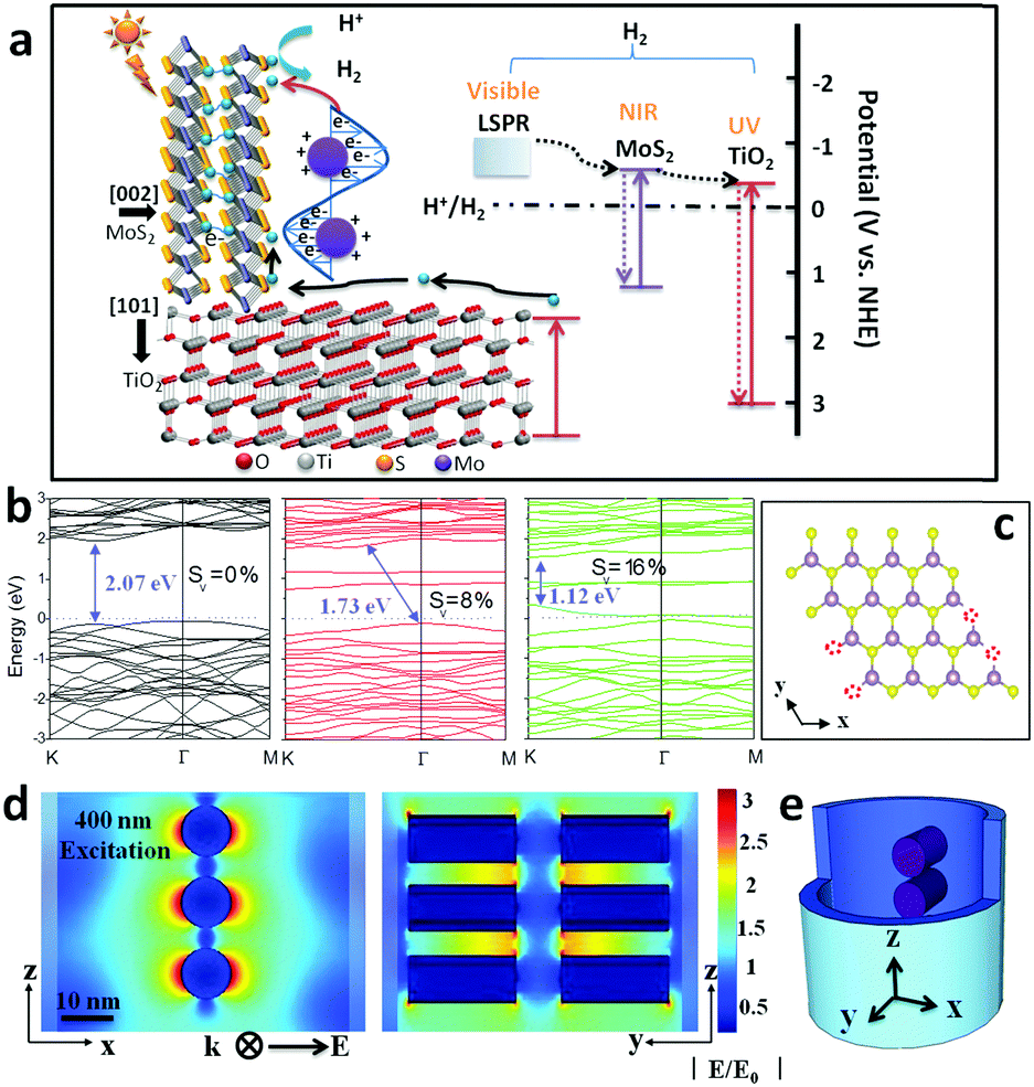 | ||
| Fig. 5 (a) Schematic diagram of the energy band structure, plasmonic resonance and electron transfer pathway in the MoS2@TiO2 heterojunction. (b) Band structure of monolayer 2H-MoS2 with 0%, 8% and 16% S-vacancies, with the valence band maximum and conduction band minimum both at the K point. (c) The model used for band gap computation by DFT (4 × 4 unit cell). (d) FEM simulation of the near-field electric field distribution inside MoS2@TiO2 heterostructures excited by a 400 nm laser and (e) a 3D-simplified model used for FEM simulation. | ||
To have an insightful understanding of the inter-band excitation of MoS2 nanoflakes and eliminate the possibility of MoS2 intrinsic activity in visible-light, the electronic band structure was calculated by density functional theory (DFT, Fig. 5b and Fig. S9a–c, details about the calculation method are given in the ESI†). S-depletion was introduced in the computation models with an atom content of 0%, 8%, and 16%, respectively, mainly at the edge position (Fig. 5c). A fundamental band gap of around 2.07 eV is found here for a perfect MoS2 crystal, with the highest occupied valence band and the lowest empty conduction band located at 1.63 eV and −0.4 eV, accordingly (Fig. 5b). The band structure is modulated by introduction of a S-vacancy, which induces the narrowing of the band gap to 1.73 (8%) and 1.12 eV (16%). Moreover, defect states appear near to the Fermi level for the model with 16% S-depletion, which improves the metallic feature and charge mobility of S-depleted MoS2 layers.20 The overall electronic density of states (DOS) for MoS2 before and after S-depletion are shown in Fig. S9a–c (ESI†). Defect states near to the Fermi level originate mainly from the d orbitals of Mo and p orbital of S atoms (Fig. S9c, ESI†), creating pseudo-ballistic electron transport channels within MoS2. This result is further supported by other literature and fully compatible with our optical spectra in the IR region (Fig. S9d, ESI†), where the MoS2 band gap absorption peaks are located around 882 nm (1.40 eV).34 A further conclusion can be deduced from the discussion aforementioned that solar light caused activity of MoS2@TiO2 films mainly functionalized by the plasmonic effect surrounding the MoS2 surface.
To further confirm this assumption, wavelength-dependent photocatalysis and finite element method (FEM) simulations were performed on MoS2@TiO2 heterostructures under monochromatic light illumination (350–700 nm, with a 50 nm interval). A spectrum dependent H2 evolution rate is revealed over the UV-vis-NIR region, with a consistent variation in absorption spectra for the MoS2@TiO2 (Fig. 4a and e). The largest H2 yield rate is about 59, 73, and 86 μmol h−1 mW−1 cm−2 for Mo loading of 10, 20 and 30 nm, respectively, located at 450, 500, and 550 nm accordingly. The relative consistency of photo-absorption and H2 production over solar light indicates that the photocatalytic activity enhancement is primarily driven by the plasmonic effect from blue-green wavelengths. Upon excitation by monochromatic light irradiation, the H2 yield is found to be higher than that with the equivalent solar light (AM 1.5 100 mW cm−2) excitation, especially in the 400–600 nm region. This suggests an additional benefit for use of variant colored light for plasmonic material based H2 generation. A diagrammatic simulation (FEM) of electric field distribution at MoS2 nanoflake vicinities is shown in Fig. 5d and Fig. S10 (ESI†). A 3D model was designed using a single TiO2 nanocavity (50 nm in diameter and 70 nm in length) and three vertically loaded MoS2 nanorods (10 nm in diameter and 20 nm in length) on both sides (Fig. 5e). It was found that light irradiation coupled with LSPR yields strong electric field enhancements at the tip of MoS2. The field intensity increases with wavelength from 300 to 400 nm and reduces significantly after 500 nm, correlating with the LSPR absorption spectra of the MoS2(10)@TiO2 film (Fig. 4a). The maximum electric field enhancement is produced at 400 nm illumination (Fig. 5d). Field intensity between each antinode covers a distance longer than 5 nm, achieving zero-gap field distribution between the MoS2 interspace (<10 nm). Consequently, a 3D electric field distribution is built throughout the networked MoS2 laminate heterostructure and responds strongly to photocatalytic H2 production.
Prospectively, H2 generation from seawater will be highly desirable. However, few studies have focused on practical photocatalysis on natural seawater because of the barrier blocking of dissolved salt for photocatalytic activity and durability of catalysts.35 Here we investigated the effect of salt (mainly NaCl) on the photocatalytic activity of MoS2@TiO2 films with natural seawater (pH: 8.4) splitting under simulated solar light. As expected, the activity from seawater decreased markedly compared to that of pure water (Fig. 4c and d), because the isoelectric point of MoS2 is lower than 7 due to the plasmonic “hot” electrons on the surface. The electrostatic adherence of hydroxyl groups and metal ions and the oxidation of sulfides take place severely in seawater with a weak alkaline environment. Fortunately, 60% of incipient production is kept for samples, where the highly-ordered architecture may be helpful. This control experiment permits our MoS2@TiO2 heterostructure as a promising material for H2 production from seawater.
4. Conclusions
In summary, novel MoS2@TiO2 laminate heterostructures were synthesized by a facile process that combines anodization, PVD, and CVD. Such structures displayed intense LSPR throughout regulating the S stoichiometry of the MoS2 surfaces. The MoS2@TiO2 co-catalysts showed nearly full-solar-spectrum absorption and superb photocatalytic activity for H2 evolution. Samples with a 30 nm Mo coating enabled a H2 yield rate as high as 181 μmol h−1 cm−2, based on the synergistic plasmonic effect with homogeneity promoting charge-carrier separation and higher conductivity of “hot” electrons in this highly ordered architecture. FEM simulation and DFT calculations were performed to understand this nonmetal plasmonic system and simultaneously derive light harvesting, charge separation and transfer dynamics. Such materials, structures, and design schemes can have significant impact in using plasmonic materials for cost effective solar energy conversion.Conflicts of interest
There are no conflicts to declare.Acknowledgements
This work was financially supported by the University of Central Florida through a startup grant (no. 20080741). STEM, EELS, and XPS data analysis were supported by the U.S. Department of Energy (DOE), Office of Science, Office of Basic Energy Sciences, Early Career Research Program under award # 68278. A portion of the work was performed at the W. R. Wiley Environmental Molecular Sciences Laboratory, a DOE User Facility sponsored by the Office of Biological and Environmental Research and located at the Pacific Northwest National Laboratory.Notes and references
- J. Zhang, X. Jin, P. I. Morales-Guzman, X. Yu, H. Liu, H. Zhang, L. Razzari and J. P. Claverie, ACS Nano, 2016, 10, 4496 CrossRef CAS PubMed.
- K. Liang, Y. Yan, L. Guo, K. Marcus, Z. Li, L. Zhou, Y. Li, R. Ye, N. Orlovskaya, Y.-H. Sohn and Y. Yang, ACS Energy Lett., 2017, 2, 1315 CrossRef CAS.
- X. Zhang, Y. L. Chen, R.-S. Liu and D. P. Tsai, Rep. Prog. Phys., 2013, 76, 046401 CrossRef PubMed.
- Y.-C. Pu, G. Wang, K.-D. Chang, Y. Ling, Y.-K. Lin, B. C. Fitzmorris, C.-M. Liu, X. Lu, Y. Tong, J. Z. Zhang, Y.-J. Hsu and Y. Li, Nano Lett., 2013, 13, 3817 CrossRef CAS PubMed.
- L. Guo, Z. Li, K. Marcus, S. Navarro, K. Liang, L. Zhou, P. D. Mani, S. J. Florczyk, K. R. Coffey, N. Orlovskaya, Y.-H. Sohn and Y. Yang, ACS Sensors, 2013, 2, 621 CrossRef PubMed.
- H. He, J. Lin, W. Fu, X. Wang, H. Wang, Q. Zeng, Q. Gu, Y. Li, C. Yan, B. K. Tay, C. Xue, X. Hu, S. T. Pantelides, W. Zhou and Z. Liu, Adv. Energy Mater., 2016, 6, 1600464 CrossRef.
- W. Zhou, Z. Yin, Y. Du, X. Huang, Z. Zeng, Z. Fan, H. Liu, J. Wang and H. Zhang, Small, 2013, 9, 140 CrossRef CAS PubMed.
- K. Liang, L. Li and Y. Yang, ACS Energy Lett., 2017, 2, 373 CrossRef CAS.
- S. Gao, G.-D. Li, Y. Liu, H. Chen, L.-L. Feng, Y. Wang, M. Yang, D. Wang, S. Wang and X. Zou, Nanoscale, 2015, 7, 2306 RSC.
- Y. Liu, Y.-X. Yu and W.-D. Zhang, J. Phys. Chem. C, 2013, 117, 12949 CAS.
- H. Fei, Y. Yang, X. Fan, G. Wang, G. Ruan and J. M. Tour, J. Mater. Chem. A, 2015, 3, 5798 CAS.
- Y. Yang, H. Fei, G. Ruan, Y. Li and J. M. Tour, Adv. Funct. Mater., 2015, 25, 6199 CrossRef CAS.
- X. Liu, Z. Xing, H. Zhang, W. Wang, Y. Zhang, Z. Li, X. Wu, X. Yu and W. Zhou, ChemSusChem, 2016, 9, 1118 CrossRef CAS PubMed.
- M. J. Islam, D. A. Reddy, N. S. Han, J. Choi, J. K. Song and T. K. Kim, Phys. Chem. Chem. Phys., 2016, 18, 24984 RSC.
- L. Liang and V. Meunier, Nanoscale, 2014, 6, 5394 RSC.
- M. Ye, D. Winslow, D. Zhang, R. Pandey and Y. K. Yap, Photonics, 2015, 2, 288 CrossRef CAS.
- J. Shi, Y. Zhang, Y. Hu, X. Guan, Z. Zhou and L. Guo, J. Alloys Compd., 2016, 688, 368 CrossRef CAS.
- Q. Li, N. Zhang, Y. Yang, G. Wang and D. H. Ng, Langmuir, 2014, 30, 8965 CrossRef CAS PubMed.
- M. M. Ali and K. N. Y. Sandhya, New J. Chem., 2016, 40, 8123 RSC.
- H. Li, C. Tsai, A. L. Koh, L. Cai, A. W. Contryman, A. H. Fragapane, J. Zhao, H. S. Han, H. C. Manoharan, F. Abild-Pedersen, J. K. Nørskov and X. Zheng, Nat. Mater., 2016, 15, 48 CrossRef CAS PubMed.
- Y. Kang, S. Najmaei, Z. Liu, Y. Bao, Y. Wang, X. Zhu, N. J. Halas, P. Nordlander, P. M. Ajayan, J. Lou and Z. Fang, Adv. Mater., 2014, 26, 6467 CrossRef CAS PubMed.
- U. Ahuja, A. Dashora, H. Tiwari, D. C. Kothari and K. Venugopalan, Comput. Mater. Sci., 2014, 92, 451 CrossRef CAS.
- I. Minguez-Bacho, M. Courté, H. J. Fan and D. Fichou, Nanotechnology, 2015, 26, 185401 CrossRef PubMed.
- H. Cheng, X. Qian, Y. Kuwahara, K. Mori and H. Yamashita, Adv. Mater., 2015, 27, 4616 CrossRef CAS PubMed.
- L. P. Hansen, Q. M. Ramasse, C. Kisielowski, M. Brorson, E. Johnson, H. Topsøe and S. Helveg, Angew. Chem., Int. Ed., 2011, 50, 10153 CrossRef CAS PubMed.
- Y. Yang, H. Fei, G. Ruan, C. Xiang and J. M. Tour, Adv. Mater., 2014, 26, 8163 CrossRef CAS PubMed.
- Z. Zhang, J. Huang, Y. Fang, M. Zhang, K. Liu and B. Dong, Adv. Mater., 2017, 29, 1606688 CrossRef PubMed.
- L. Lin, N. Miao, Y. Wen, S. Zhang, P. Ghosez, Z. Sun and D. A. Allwood, ACS Nano, 2016, 10, 8929 CrossRef CAS PubMed.
- L. Guo, K. Liang, K. Marcus, Z. Li, L. Zhou, P. D. Mani, H. Chen, C. Shen, Y. Dong, L. Zhai, K. R. Coffey, N. Orlovskaya, Y.-H. Sohn and Y. Yang, ACS Appl. Mater. Interfaces, 2016, 8, 34970 CAS.
- J. Wu, X. Lu, Q. Zhu, J. Zhao, Q. Shen, L. Zhan and W. Ni, Nano-Micro Lett., 2014, 6, 372 CrossRef CAS.
- K. R. Catchpole and A. Polman, Opt. Express, 2008, 16, 21793 CrossRef CAS PubMed.
- J. H. Heo, D. H. Song, B. R. Patil and S. H. Im, Isr. J. Chem., 2015, 55, 966 CrossRef CAS.
- H. S. Jung and N.-G. Park, Small, 2015, 11, 10 CrossRef CAS PubMed.
- Y. Han, T. Hu, R. Li, J. Zhou and J. Dong, Phys. Chem. Chem. Phys., 2015, 17, 3813 RSC.
- Y. Li, D. Gao, S. Peng, G. Lu and S. Li, Int. J. Hydrogen energy, 2011, 36, 4291 CrossRef CAS.
Footnote |
| † Electronic supplementary information (ESI) available: Morphological and structure characterization, photo-response and photo-catalysis performance. See DOI: 10.1039/c7ee02464a |
| This journal is © The Royal Society of Chemistry 2018 |