
Enhanced performances of planar heterojunction organic light-emitting diodes via diluting an n-type transporter into a carbazole-based matrix†
Dongcheng
Chen
*,
Binbin
Li
,
Lin
Gan
,
Xinyi
Cai
,
Yuguang
Ma
 ,
Yong
Cao
and
Shi-Jian
Su
*
,
Yong
Cao
and
Shi-Jian
Su
*
State Key Laboratory of Luminescent Materials and Devices and Institute of Polymer Optoelectronic Materials and Devices, South China University of Technology, Guangzhou 510640, P. R. China. E-mail: mschendc@scut.edu.cn; mssjsu@scut.edu.cn
First published on 27th November 2017
Abstract
Electroluminescence originating from layer-to-layer charge transfer (LLCT) in organic light-emitting diodes (OLEDs) was early observed, whereas, the inferior performances limit their practical applications. In this work, we demonstrated an efficient approach to improve the overall performances of LLCT-based planar heterojunction OLEDs by simply diluting an n-type electron transport material into a carbazole-based matrix material to suppress excited-state quenching. As a result, an optimized device with a peak current efficiency of 41 cd A−1 (corresponding to a maximum external quantum efficiency of 12.6%) exhibited significantly enhanced efficiencies and much higher brightness at high current densities in contrast to the control devices without a mixture layer. We illustrated that even with a similar narrow recombination region, it is feasible to achieve excellent fluorescent OLEDs with light emission originating from LLCT. We believe that this work should pave the way for developing high-performance LLCT-based OLEDs with a high efficiency, reduced efficiency roll-off and sufficiently large maximum brightness.
Introduction
Organic light-emitting diodes (OLEDs) have been widely applicable in display products, such as mobile phones and televisions, and show great application potential in the field of solid-state lighting. Generally, the device structure of an OLED consists of an independent emission layer (EML) and adjacent functional layers, such as hole and electron transport layers (HTLs, ETLs). Light emission from an OLED is generally as a result of energy release from the excited state that is formed in the EML (Fig. 1a). Alternatively, electroluminescence (EL) could also be generated by a layer-to-layer charge transfer (LLCT) process. LLCT involves an electronic transfer process that occurs between two adjacent layers (Fig. 1b). The LLCT emission upon optical excitation is spectrally different from those of bulk materials, and belongs to the scope of exciplex emission (i.e., interface exciplex); while upon electrical excitation, LLCT emission originates from the process involving electron migration from an n-type material to a p-type material, intermediated by an exciton state. The EL phenomenon from LLCT was, in fact, observed early. However, this EL event was generally deemed as a fatal factor to lower device performances.1,2 Subsequent investigations revealed that the LLCT mechanism might be a possible approach to fabricate OLEDs. e.g., Berggren et al. reported white OLEDs with partial light emission originating from LLCT between the HTL and the ETL.3 Quite pure LLCT emission from polymer-based devices was also reported by Gebler et al.4 Though emission from LLCT was frequently observed in OLEDs,5–12 the overall performances of these devices were not promising enough to support their practical application.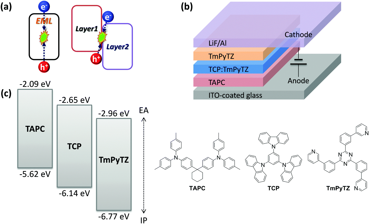 | ||
| Fig. 1 (a) Schematic diagram of electronic processes of light generation from OLEDs with an independent EML and layer-to-layer charge transfer between two layers; (b) schematic layer configuration of the devices in this study; (c) energy levels and molecular structures of the used organic materials. | ||
Recent works by Adachi et al. demonstrated that exciplex-based OLEDs with a mixed donor:acceptor (D:A) EML that exhibits thermally-activated delayed fluorescence (TADF) could be theoretically highly efficient due to the capacity of harvesting both singlet and triplet excitons for radiative utilization.13,14 Inspired by these works, there have been many reports about efficient exciplex OLEDs employing a binary-mixed EML.15–19 In the view of the microcosmic level, LLCT exciplex emission from a bilayer planar heterojunction may be analogous to the case of exciplex emission originating from a D:A mixture layer, since both processes occur bi-molecularly based on a similar intermolecular charge transfer mechanism. Thereby, OLEDs with light emission originating from LLCT might show comparable performances in contrast to the exciplex OLEDs using an independent D:A mixture EML. However, in practice, the performances of the former are dramatically lower than the latter, even though they use the same D and A materials. LLCT-based OLEDs typically show low efficiencies and low maximum brightness. The efficiency drawback is more remarkable when the device is at a high current density, which makes the efficiencies at higher luminance extremely low.
The macroscopic physical morphology of LLCT systems based on stacked, planar heterojunctions is totally different to the case of binary-mixed counterparts with a bulk heterojunction configuration. This difference in layer construction should result in variation of the condensed state properties, which might be relevant to the carrier and excitonic behaviours. There is still a lack of investigation of key factors leading to the inferior performances of LLCT-based OLEDs. Our previous results showed that selection of appropriate p- and n-type material systems should significantly affect the resulting device performances, suggesting that progress of materials, especially n-type materials, and their combination strategies should help to improve performances of LLCT-based devices.20 High efficiency yellow and green planar pn heterojunction OLEDs with a peak EQE value above 10% were demonstrated based on an extremely simplified device structure. However, efficiencies at high current densities and the maximum luminance are still moderate for the resulting devices.20 In terms of device physics, there is a common viewpoint that a narrow carrier recombination and exciton generation region for these kinds of devices should be fatal to the EL performances.21–23 Compared with the conventional OLEDs with an independent EML, in which the excited state could be widely dispersed within the EML, the carriers and excitons can only aggregate at a very thin interface because of the planar contact heterojunction configuration. The narrow carrier recombination region is generally, empirically regarded as the intrinsic nature limiting the overall performances of LLCT-based EL devices.
In this work, we demonstrated efficient planar heterojunction OLEDs with light emission originating from LLCT, through introducing a carbazole-based matrix material into the n-type transport layer to suppress the excited-state quenching effect. Based on this strategy, high performance fluorescent OLEDs were fabricated with a peak current efficiency (CE) of 41 cd A−1, a maximum external quantum efficiency (EQE) of 12.6% and a greatly enhanced efficiency at higher current densities in contrast to the control devices without a mixture layer. The improved device performance can be attributed to the suppression of the excited-state quenching effect. From this prototype investigation, we proposed that even with a narrow carrier recombination region, it is feasible to achieve excellent fluorescent OLEDs with light emission originating from LLCT with an approximate device configuration. We believe that this should be a widely applicable and effective method for enhanced efficiency, especially at higher current densities, and maximum brightness to construct efficient planar heterojunction OLEDs with light emission originating from LLCT.
Experimental section
General details
4,4′-Cyclohexylidenebis[N,N-bis(4-methylphenyl)aniline] (TAPC) and 1,3,5-tri(9H-carbazol-9-yl)benzene (TCP) were purchased from Luminescence Technology Corp. (Lumtec, Taiwan) and used without further purification. TmPyTZ was synthesized in our lab according to the previously-reported ref. 24. Ionization potentials of the film samples were measured using an atmospheric ultraviolet photoelectron spectroscope (Rikken Keiki, AC-3). UV-vis absorption spectra were measured using a spectrophotometer (Shimadzu, UV-3600). Fluorescence and phosphorescence spectra of the samples in toluene solution were measured at room temperature and at 77 K with a delay time of 1 ms, respectively, based on a spectrometer equipped with a gate-control phosphorescence accessory (HORIBA Jobin Yvon, FL-3). Steady state and transient photoluminescence (PL) and transient EL spectra of the film samples and devices were measured using a spectrometer equipped with a time-correlated single photon counting (TCSPC) component (FL980, Edinburgh Instruments).Device fabrication and characterization
Patterned 95 nm-thin indium tin oxide (ITO)-coated glasses were used as the substrates to fabricate devices. ITO substrates were cleaned in sequence using an ultrasonic bath of acetone, detergent, deionized water, isopropyl alcohol and then dried at 80 °C for more than 3 h. The devices were fabricated by step-by-step deposition of various functional layers under an unbroken vacuum of <4 × 10⁻⁴ Pa. The light emissive area of the devices was masked to be 0.09 cm2. Current density–voltage–luminance (J–V–L) characteristics of the OLEDs were measured using a Keithley source-measure unit (model: 2400) and a Konica Minolta chromameter (model: CS-200). The EL spectra of the devices were measured using a spectrophotometer (Photo Research, Model: SpectraScan PR-705). EQEs are calculated from the current densities, CEs, and their corresponding EL spectra, provided that the emission of the OLEDs follows a Lambertian distribution.Results and discussion
The PL emission spectra of TAPC, TCP and the binary-mixed films, TAPC![[thin space (1/6-em)]](https://www.rsc.org/images/entities/char_2009.gif) :TmPyTZ (1:1, molar ratio) and TCP:TmPyTZ (1:1, molar ratio) are plotted in Fig. 2a (PL emission of the TmPyTZ film is beyond the detection limit). Their transient PL decay curves are shown in Fig. S1 (ESI†). Red-shifted emission in contrast to those of the individual films can be observed for both TAPC:TmPyTZ and TCP:TmPyTZ samples, with a peak charge transfer emission energy (CT1) of 2.93 and 2.25 eV, respectively. Prolonged excitonic lifetimes of the mixture samples can also be verified from the transient PL results compared with the single-component films. These results indicate the existence of new excited-state charge transfer (i.e., exciplex) emission for these two D:A systems. TAPC and TmPyTZ combinations have been studied with a typical TADF character previously,20 and thus are adopted as an example of the LLCT emission system here. Fig. 2b depicts the fluorescence and phosphorescence spectra of TAPC, TCP and TmPyTZ in toluene, respectively. Their lowest singlet excited state (S1) values can be extracted from the first high-energy emission peak of the fluorescence spectra, which are 3.28, 3.45 and 3.41 eV for TAPC, TCP and TmPyTZ, respectively. Similarly, their extracted lowest triplet excited state (T1) values from the phosphorescence spectra are 2.95, 3.02 and 2.84 eV, respectively. Both S1 and T1 values for TAPC, TCP and TmPyTZ are larger than CT1 of TAPC:TmPyTZ (2.25 eV), which can suppress the endothermic back energy transfer process.
:TmPyTZ (1:1, molar ratio) and TCP:TmPyTZ (1:1, molar ratio) are plotted in Fig. 2a (PL emission of the TmPyTZ film is beyond the detection limit). Their transient PL decay curves are shown in Fig. S1 (ESI†). Red-shifted emission in contrast to those of the individual films can be observed for both TAPC:TmPyTZ and TCP:TmPyTZ samples, with a peak charge transfer emission energy (CT1) of 2.93 and 2.25 eV, respectively. Prolonged excitonic lifetimes of the mixture samples can also be verified from the transient PL results compared with the single-component films. These results indicate the existence of new excited-state charge transfer (i.e., exciplex) emission for these two D:A systems. TAPC and TmPyTZ combinations have been studied with a typical TADF character previously,20 and thus are adopted as an example of the LLCT emission system here. Fig. 2b depicts the fluorescence and phosphorescence spectra of TAPC, TCP and TmPyTZ in toluene, respectively. Their lowest singlet excited state (S1) values can be extracted from the first high-energy emission peak of the fluorescence spectra, which are 3.28, 3.45 and 3.41 eV for TAPC, TCP and TmPyTZ, respectively. Similarly, their extracted lowest triplet excited state (T1) values from the phosphorescence spectra are 2.95, 3.02 and 2.84 eV, respectively. Both S1 and T1 values for TAPC, TCP and TmPyTZ are larger than CT1 of TAPC:TmPyTZ (2.25 eV), which can suppress the endothermic back energy transfer process.
 | ||
| Fig. 2 (a) PL emission spectra of neat films and binary-mixed films (1:1, molar ratio); (b) fluorescent and phosphorescent emission spectra of the materials in toluene. | ||
The schematic device configurations are shown in Fig. 1b. Detailed device structures are as follows: ITO/TAPC (45 nm)/TCP:x mol% TmPyTZ (x = 0, 5, 10, 20, 30, 40, 50, 65, 80, or 100, 20 nm)/TmPyTZ (75 nm)/LiF (1 nm)/Al (120 nm), where these devices are denoted as D1, D2, D3, D4, D5, D6, D7, D8, D9, D10, respectively. D1 and D10 without a mixture layer play a role as the control devices. TCP was used as the diluting spacer matrix material. The concentration of TmPyTZ in the mixture layer was increased from 0% (pure TCP) to 100% (pure TmPyTZ) with a corresponding reduction in the concentration of TCP, aiming at probing the concentration-dependent effect. Fig. 3a displays their J–V characteristics. It can be seen that as the doping ratio of TmPyTZ in the binary mixture film gradually increases from 0% to 30%, the injection current density dramatically increases. While the mixing proportion is further increased above 30%, the increase of current densities tends to be slow. A similar changing trend of current densities as a function of doping ratio was also observed by Ha et al, while they investigated current densities of the devices employing a TCTA–BmPyPB mixture.25 From their energy levels (Fig. 1c, for details to determine the energy level data refer to Fig. S2, ESI†), it can be deduced that electron transport in the mixture layer should be preferred on the TmPyTZ channel because of its higher electron affinity (EA) in contrast to that of TCP (2.96 vs. 2.65 eV). The dependence of current densities on the mixing ratio of TmPyTZ can be explained by the percolation transport theory.25–27 With an increase in doping ratios of TmPyTZ, an intersecting network for electron transport can be formed. Thereby, percolating materials can govern the charge transport in a wide range of concentrations. As the doping fraction exceeds 30%, the transport capacities of the percolating materials in the mixture layer get close, thus, the current densities in the devices with a mixing ratio of TmPyTZ above 30% tend to be analogous. At a high doping ratio of TmPyTZ, the electron flux can be well transported within the mixture layer. This can eliminate layer-to-layer electron injection barriers between the mixture layer and the pure TmPyTZ ETL layer, and make electron carriers be captured at the interface between the mixture layer and the HTL. As for the cases of low doping ratios, there are two approaches for carrier capture and exciton generation. The electron carriers can migrate by the TmPyTZ channel formed in the mixture layer, leading to exciton generation at the interface between the mixture layer and the HTL. On the other hand, holes can also be injected from the TAPC layer into the TCP channel via overcoming the layer-to-layer energy barriers under high electric fields, leading to exciton generation with the encounter of electrons from the TmPyTZ channel. Whereas, for a device with a pure TCP layer, electron carriers should accumulate at the TCP/ETL interface, because of a rather big electron injection barrier from TmPyTZ to TCP, and then holes are injected from TAPC into TCP, which leads to exciton generation at the TCP/ETL interface.
 | ||
| Fig. 3 (a) J–V and (b) L–V characteristics of the devices from D1 to D10 as a function of different TmPyTZ ratios in the binary mixture layer. | ||
These analyses can be directly proved by the luminance–current density (L–V) characteristics (Fig. 3b) and the EL spectra results under various current densities (Fig. 4). The emissions of D1 with a pure TCP layer mainly arise from the TCP/TmPyTZ interface. This confirms that holes are injected across the TCP layer and recombined with electrons at the TCP/TmPyTZ interface. The large injection barriers from TAPC to TCP render D1 with the largest driving voltages among all these devices. Deep blue emission was observed for D1, indicating that deep blue OLEDs based on the LLCT mechanism should be possible. The EL spectra of D2 show two obviously distinct emission bands. The high-energy band peaking at around 430 nm should be attributed to LLCT emission due to the TCP/TmPyTZ interactions, while the low-energy emission band should arise from that of the TAPC/TmPyTZ system. The high-energy band tends to be dominant at high current densities. This can be explained by the fact that more hole carriers can be injected into the TCP channels in the mixtures under large electric fields and thus provide more emission arising due to the TCP/TmPyTZ interactions. As the TmPyTZ proportions in the mixture layer are gradually enhanced, the high-energy emission band of the resulting devices dramatically reduces, meanwhile, the driving voltages also simultaneously decline. While in the devices having a mixture layer with TmPyTZ concentrations equal to or above 30% (D5–9), EL emission due to the TCP/TmPyTZ interactions almost disappears. This is because most of the electrons migrate to the TAPC/mixture interface by percolating the TmPyTZ channel formed in the mixture layer, thus offering nearly pure LLCT emissions due to TAPC and TmPyTZ interactions, which are identical to the emission of the device without TCP (D10). Owing to the avoidance of layer-to-layer injection barriers, the devices from D5 to D9 also exhibit similar driving voltages with respect to those of D10. These results are consistent with the previous analyses based on their energy levels and J–V characteristics. According to the above results, TCP should not be involved in carrier transport and the exciton generation process in the devices with a high fraction of TmPyTZ (D5–9), i.e., TCP plays the role of a diluting spacer without being involved in the carrier and exciton processes in these devices.
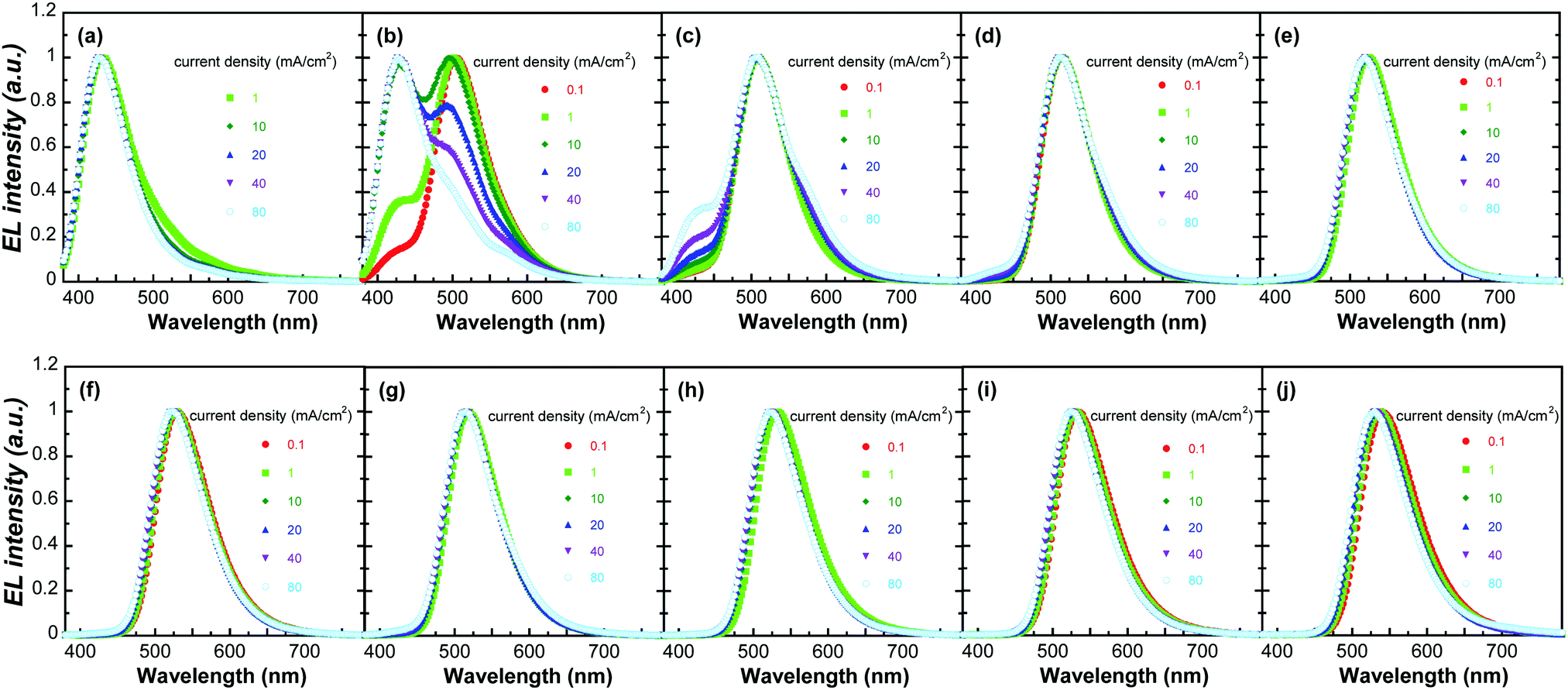 | ||
| Fig. 4 EL emission spectra under various current densities of the devices (a) D1, (b) D2, (c) D3, (d) D4, (e) D5, (f) D6, (g) D7, (h) D8, (i) (D9) and (j) D10. | ||
CE, power efficiency (PE) and EQE data are, respectively, plotted in Fig. 5a–c as a function of current densities, and their key performance parameters are summarized in Table 1. D1 exhibits a maximum EQE of 0.34%. The low efficiency is attributed to the inferior luminescent property of the TCP/TmPyTZ exciplex system. With the increasing doping fractions of TmPyTZ in the mixture layer, the efficiencies of the devices are significantly increased, owing to the enhanced contribution from the TAPC/TmPyTZ emission. The maximum EQE of D5 reaches 11.0%. For D5, D6, D7, their maximum EQEs remain nearly constant, while the peak efficiencies of D8–10 show a decreasing trend. D10 without any TCP component merely possesses a maximum EQE of 7.13%, which is around 30% lower than the efficiencies of D5, D6 and D7. These results demonstrated that through diluting TmPyTZ into the TCP matrix with an appropriate fraction the efficiency of the resulting devices could be significantly enhanced. Meanwhile, the maximum luminance values of D5–D7 are 3625, 3278, 3542 cd m−2, respectively, which are about 25 fold larger than that of D10 (122.4 cd m−2). Prior results show that the thickness of the transport layer can affect their device performances obviously,20 thus, we further optimized the devices by tuning the thickness of the TAPC layer. It was observed that the thickness of the TAPC layer obviously affects the device performances, probably because of modulation of the carrier balance.20 Accordingly, on the basis of a 75 nm-thin TAPC layer as a HTL, the performance of the device employing a TmPyTZ:50% TCP layer can be further improved, with maximum EQE, CE, PE and luminance of 12.6%, 41.0 cd A−1, 53.7 lm W−1 and 3578 cd m−2, respectively (Table 1, for detailed performance data of these devices refer to Fig. S3, ESI†).
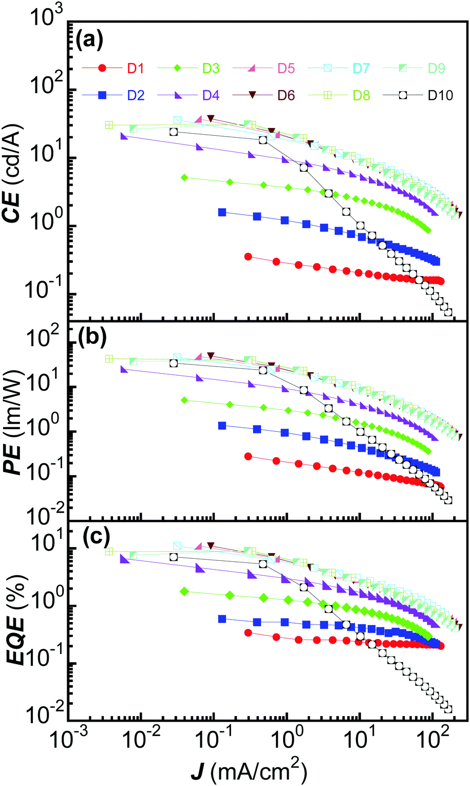 | ||
| Fig. 5 Efficiency performances of the developed devices: (a) CE–J, (b) PE–J and (c) EQE–J characteristics. | ||
| Devices | V on | Maximum efficiency | L max (cd m−2) | CIEx,yb | λ peak (nm) | ||
|---|---|---|---|---|---|---|---|
| CE (cd A−1) | EQE (%) | PE (lm W−1) | |||||
| a Driving voltage where the electroluminescence is 1 cd m−2. b At a current density of 1 mA cm−2. | |||||||
| D1 | 4.0 | 0.36 | 0.34 | 0.28 | 199.7 | (0.173, 0.124) | 430 |
| D2 | 3.5 | 1.59 | 0.60 | 1.38 | 333.0 | (0.211, 0.384) | 426, 502 |
| D3 | 3.1 | 5.15 | 1.78 | 5.05 | 1331 | (0.231, 0.501) | 426, 510 |
| D4 | 2.6 | 21.0 | 6.66 | 25.3 | 2948 | (0.259, 0.556) | 516 |
| D5 | 2.1 | 37.1 | 11.0 | 48.5 | 3625 | (0.303, 0.590) | 526 |
| D6 | 2.1 | 37.7 | 11.0 | 49.3 | 3278 | (0.318, 0.592) | 530 |
| D7 | 2.1 | 37.6 | 11.1 | 49.2 | 3542 | (0.316, 0.590) | 526 |
| D8 | 2.1 | 30.8 | 9.00 | 40.3 | 3161 | (0.338,0.591) | 532 |
| D9 | 2.1 | 31.2 | 9.10 | 40.9 | 2832 | (0.335, 0.591) | 530 |
| D10 | 2.1 | 24.2 | 7.13 | 34.6 | 122.4 | (0.360, 0.584) | 536 |
| D7 (55 nm TAPC) | 2.2 | 38.8 | 11.9 | 50.8 | 2981 | (0.376, 0.572) | 540 |
| D7 (65 nm TAPC) | 2.2 | 39.8 | 12.1 | 52.1 | 3010 | (0.387, 0.568) | 544 |
| D7 (75 nm TAPC) | 2.2 | 41.0 | 12.6 | 53.7 | 3578 | (0.399, 0.561) | 550 |
We note that the exciton recombination regions for these devices are extremely narrow, in the consideration of the light emission originating from LLCT at a planar heterojunction. Compared with the control device, D10, the exciton recombination areas for the devices with a mixture diluting layer should be even smaller, because the TmPyTZ molecules that are in contact with the TAPC layer to offer LLCT excited states are greatly reduced by mixing with TCP. Thus, the origins of the improvement of the maximum efficiency, reduced efficiency roll-off at high current densities and maximum luminance for the devices here should not be ascribed to the broadened carrier recombination region. These results indicate that even with a narrow carrier recombination region, it is feasible to achieve excellent fluorescent OLEDs with light emission originating from LLCT, provided that the device configuration and material systems are well modulated.
In order to clarify the origin of enhanced performances of the devices with a diluting spacer component, transient PL experiments were performed. Fig. 6a displays the transient PL decay curves of TAPC (8 nm)/TmPyTZ (10 nm) and TAPC (8 nm)/TCP:50% TmPyTZ (10 nm) films. The thin thickness of the layers facilitates the energy transfer from the local excited states to the charge transfer state. The decay curves are fitted by the following function:
| I(t) = A1e−t/τ1 + A2e−t/τ2, |
:50% TmPyTZ are 1.89% and 98.11%, respectively. To our knowledge, the proportion of the delayed component with a value above 98% was scarcely reported in the literature. Meanwhile, its lifetimes of the prompt and delayed decay components are 27 ns and 4.2 μs, respectively. From their steady-state PL spectra, it can be seen that the CT emission band for both samples should be mainly assignable to the emission of TAPC and TmPyTZ bi-molecular systems (Fig. S4, ESI†). Thus, the prolonged lifetime and enhanced proportion of the delayed components for TAPC/TCP:50% TmPyTZ indicate that the exciton quenching effect is more severe for TAPC/TmPyTZ. Through introducing TCP as a diluting matrix material, the LLCT excitons can be spatially isolated. This is beneficial for the long-lived delayed excitons with a relatively slow radiative rate to give more efficient radiative transition. Thus, we propose that the excited-state isolation effect is mainly responsible for the overall performance improvement. Thereby, the devices with a diluting mixture layer show better performances in contrast to the control device with a pure TAPC/TmPyTZ planar pn heterojunction.
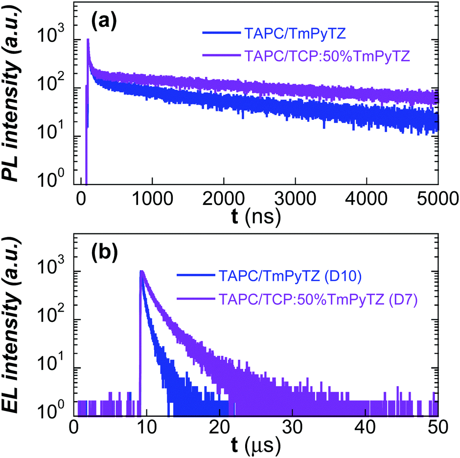 | ||
| Fig. 6 (a) Transient PL decay curves (λemi = 525 nm) of film samples consisting of TAPC (8 nm)/TmPyTZ (10 nm) and TAPC (8 nm)/TCP:50% TmPyTZ (10 nm); (b) transient EL decay curves (λemi = 530 nm) of the devices employing TAPC/TmPyTZ (D10) and TAPC/TCP:50% TmPyTZ (D7). | ||
We further conducted transient EL experiments based on the devices employing TAPC/TmPyTZ (D10) and TAPC/TCP:50% TmPyTZ (D7). As shown in Fig. 6b, D7 exhibited a much longer decay lifetime in contrast to that of D10. The prolonged EL decay lifetime of D7 should also be ascribed to the reduced excited-state quenching. This trend is consistent with the transient PL decay results. Through the above transient PL and EL measurement results, we concluded that reducing the excited-state quenching effect should be the main factor to improve the LLCT device performance. We note that this strategy might be widely applicable to enhance the device performance based on the LLCT mechanism, and this methodology might also be promoted to design p- or n-type materials to develop high-performance LLCT-based devices, e.g., chemically coupling the diluting spacer units to the compounds used for LLCT emission.
Conclusions
In summary, we demonstrated an effective approach to improve the performances of OLEDs with light emission originating from LLCT, by diluting an n-type transport material into a carbazole-based spacer matrix material (TCP). The resulting devices exhibited significantly reduced efficiency roll-off at high current densities and greatly improved maximum luminance in contrast to the control devices employing a pure organic pn heterojunction. Accordingly, the optimized device exhibited a maximum EQE of 12.6% and a maximum brightness of 3578 cd m−2. We attributed the enhanced device performances to the suppression of excited-state quenching and clarify that even with a narrow recombination region, it is feasible to achieve excellent fluorescent OLEDs with light emission originating from LLCT with an approximate device configuration. We believe that our work should shed light on developing high-performance fluorescent OLEDs with light originating from LLCT with a high efficiency, reduced efficiency roll-off and enhanced retainable brightness.Conflicts of interest
There are no conflicts to declare.Acknowledgements
The authors greatly appreciate the financial support from the National Key R&D Program of China (2016YFB0401004), 973 Project (2015CB655003), the National Natural Science Foundation of China (51625301, 51603071, 51573059 and 91233116), the China Postdoctoral Science Foundation (2016M590775, 2017T100628), and Guangdong Provincial Department of Science and Technology (2016B090906003 and 2016TX03C175).Notes and references
- C. Adachi, T. Tsutsui and S. Saito, Appl. Phys. Lett., 1990, 56, 799 CrossRef CAS.
- Y. Takakazu, I. Tetsuji and K. Takaki, Jpn. J. Appl. Phys., 1994, 33, L250 Search PubMed.
- M. Berggren, G. Gustafsson, O. Inganas, M. R. Andersson, T. Hjertberg and O. Wennerstroem, J. Appl. Phys., 1994, 76, 7530 CrossRef CAS.
- D. D. Gebler, Y. Z. Wang, D. K. Fu, M. Swager and A. J. Epstein, J. Chem. Phys., 1998, 108, 7842 CrossRef CAS.
- C. I. Chao and S. A. Chen, Appl. Phys. Lett., 1998, 73, 426 CrossRef CAS.
- J. F. Wang, Y. Kawabe, S. E. Shaheen, M. M. Morrell, G. E. Jabbour, P. A. Lee, J. Anderson, N. R. Armstrong, B. Kippelen, E. A. Mash and N. Peyghambarian, Adv. Mater., 1998, 10, 230 CrossRef CAS.
- Y. Kawabe and J. Abe, Appl. Phys. Lett., 2002, 81, 493 CrossRef CAS.
- X. Z. Jiang, M. S. Liu and A. K. Y. Jen, J. Appl. Phys., 2002, 91, 10147 CrossRef CAS.
- S. P. Singh, Y. N. Mohapatra, M. Qureshi, S. Sundar Manoharan and S. S. Manoharan, Appl. Phys. Lett., 2005, 86, 113505 CrossRef.
- A. P. Kulkarni and S. A. Jenekhe, J. Phys. Chem. C, 2008, 112, 5174 CAS.
- S. Y. Yang, X. L. Zhang, Z. D. Lou and Y. B. Hou, Appl. Phys. A: Mater. Sci. Process., 2008, 90, 475 CrossRef CAS.
- M. Carvelli, A. van Reenen, R. A. J. Janssen, H. P. Loebl and R. Coehoorn, Org. Electron., 2012, 13, 2605 CrossRef CAS.
- K. Goushi, K. Yoshida, K. Sato and C. Adachi, Nat. Photonics, 2012, 6, 253 CrossRef CAS.
- K. Goushi and C. Adachi, Appl. Phys. Lett., 2012, 101, 023306 CrossRef.
- D. Chen, Z. Wang, D. Wang, Y.-C. Wu, C.-C. Lo, A. Lien, Y. Cao and S.-J. Su, Org. Electron., 2015, 25, 79 CrossRef CAS.
- X. K. Liu, Z. Chen, C. J. Zheng, C. L. Liu, C. S. Lee, F. Li, X. M. Ou and X. H. Zhang, Adv. Mater., 2015, 27, 2378 Search PubMed.
- J. Li, H. Nomura, H. Miyazaki and C. Adachi, Chem. Commun., 2014, 50, 6174 RSC.
- W. Y. Hung, G. C. Fang, S. W. Lin, S. H. Cheng, K. T. Wong, T. Y. Kuo and P. T. Chou, Sci. Rep., 2014, 4, 5161 CrossRef CAS PubMed.
- W. Y. Hung, P. Y. Chiang, S. W. Lin, W. C. Tang, Y. T. Chen, S. H. Liu, P. T. Chou, Y. T. Hung and K. T. Wong, ACS Appl. Mater. Interfaces, 2016, 8, 4811 CAS.
- D. C. Chen, G. Z. Xie, X. Y. Cai, M. Liu, Y. Cao and S. J. Su, Adv. Mater., 2016, 28, 239 CrossRef CAS PubMed.
- S. J. Lee, J. R. Koo, H. W. Lee, S. E. Lee, H. J. Yang, S. S. Yoon, J. Park and Y. K. Kim, Electron. Mater. Lett., 2014, 10, 1127 CrossRef CAS.
- R. Sheng, L. M. Zuo, K. W. Xue, Y. Duan, P. Chen, G. Cheng and Y. Zhao, J. Phys. D: Appl. Phys., 2016, 49, 335101 CrossRef.
- H. Fukagawa, K. Watanabe, T. Tsuzuki and S. Tokito, Appl. Phys. Lett., 2008, 93, 133312 CrossRef.
- S. J. Su, H. Sasabe, Y. J. Pu, K. Nakayama and J. Kido, Adv. Mater., 2010, 22, 3311 CrossRef CAS PubMed.
- D. G. Ha, J. J. Kim and M. A. Baldo, AIP Adv., 2016, 6, 045221 CrossRef.
- C. Li, L. Duan, H. Y. Li and Y. Qiu, Org. Electron., 2013, 14, 3312 CrossRef CAS.
- K. Vakhshouri, D. R. Kozub, C. C. Wang, A. Salleo and E. D. Gomez, Phys. Rev. Lett., 2012, 108, 026601 CrossRef PubMed.
- S. Hirata, Y. Sakai, K. Masui, H. Tanaka, S. Y. Lee, H. Nomura, N. Nakamura, M. Yasumatsu, H. Nakanotani, Q. S. Zhang, K. Shizu, H. Miyazaki and C. Adachi, Nat. Mater., 2015, 14, 330 CrossRef CAS PubMed.
- Q. S. Zhang, B. Li, S. P. Huang, H. Nomura, H. Tanaka and C. Adachi, Nat. Photonics, 2014, 8, 326 CrossRef CAS.
Footnote |
| † Electronic supplementary information (ESI) available: Transient PL decay curves, ultraviolet photoelectron spectra and absorption spectra, performance figures of optimized devices. See DOI: 10.1039/c7tc04459c |
| This journal is © The Royal Society of Chemistry 2018 |