
A highly efficient nano-graphite electron transport layer for high performance ZnO/Si solar cells†
Ming
Chen
ab,
Gang
Wu
a,
Minmin
Zhang
a,
Jie
Liu
 a,
Jiantao
Zai
*b,
Xuefeng
Qian
b and
Xibin
Yu
*a
a,
Jiantao
Zai
*b,
Xuefeng
Qian
b and
Xibin
Yu
*a
aThe Education Ministry Key Laboratory of Resource Chemistry, Shanghai Key Laboratory of Rare Earth Functional Materials, Department of Chemistry, Shanghai Normal University, Shanghai 200234, People's Republic of China. E-mail: xibinyu@shnu.edu.cn
bShanghai Electrochemical Energy & Research Centre, School of Chemistry and Chemical Engineering, State Key Laboratory of Metal Matrix Composites, Shanghai Jiao Tong University, Shanghai, 200240, P. R. China. E-mail: zaijiantao@sjtu.edu.cn
First published on 15th January 2018
Abstract
Photovoltaic modules are considered as the most efficient way to utilize solar energy, while the power conversion efficiencies of commercial crystalline silicon (c-Si) solar cells still need to be improved. Herein, nano-graphite was designed as a highly efficient electron transport layer in high performance ZnO/Si solar cells and prepared via a simple solution phase deposition and rapid annealing process. The ZnO QDs can broaden the range of spectral response by generating more electron–hole pairs via multiple exciton effects. The built-in-field formed between the n-type ZnO QD layer and n-type Si and highly conductive nano-graphite can accelerate the electron collection and transportation from n-type Si to the front electrode. Thus, the designed Si solar cell with nano-graphite and ZnO QD layers shows a significantly improved power conversion efficiency of 14.99% compared to the ZnO/Si solar cell (13.62%) and unmodified commercial c-Si solar cells (12.73%). This cost effective and environmentally friendly technology can be easily applied for the industrial scale production of Si solar cells.
Introduction
Crystalline silicon (c-Si) solar cells are the most popular commercial photovoltaic (PV) modules because of their acceptable power conversion efficiencies and cost derived from the high natural abundance of Si and mature processing technology.1,2 However, the power conversion efficiency of commercial c-Si solar cells (∼18%) is far from the theoretical maximum (29%), because of the optical carrier recombination, series resistance, thermal and quantum losses.3–5 The optical and recombination losses of photogenerated carriers are considered to be the main factors to limit the power conversion efficiency of solar cells. Nanostructured semiconductors with wider band gap coating layers can serve as anti-reflectance layers on c-Si solar cells and enhance the light absorption via the light trapping effects of porous or array nanostructures and the extended light response range.6,7 Additionally, the built-in-field of the semiconductor junctions between these materials and c-Si can facilitate the separation and prevent hot drifting of photocarriers. Thus, amorphous Si, Si quantum dots (QDs), ZnO, crystalline and amorphous SiC with morphologies of quantum dots,8,9 nanowires,6,10 nanorods,7,11etc. have been widely used to improve the performance of solar cells in the past few years.As a typical n-type semiconductor oxide, ZnO with a wide band gap of 3.37 eV can only absorb light mainly in the UV absorption region, which has been beneficial to the absorption of c-Si in the visible light region. Due to the efficient built-in-field between ZnO and Si, low cost and good adaptability to present processing technology of c-Si solar cells, ZnO/c-Si solar cells have received wide attention since 1995.12 Recently, different light trapping nanostructures built using 1D ZnO have been applied to enhance the power conversion efficiency of c-Si (10.9%).13 However, the power conversion efficiency still needs to be improved. Quantum dots have the ability to generate more than one photo induced electron–hole (e−–h+) pair upon the absorption of a single photon, which has been widely known as the multiple exciton effect and can offer a chance to overcome the theoretical limit of traditional solar cells.11,14–16 Therefore, ZnO quantum dots (ZnO QDs) have been considered as one of the promising candidates and serve as an efficient anti-reflection layer among the semiconductor materials for improving the power conversion efficiency of solar cells.17–19
However, the wide band gap of ZnO and the abundant surface states of ZnO QDs are not beneficial to electron conduction.15 Thus, the electron collection and transportation from n-type Si to the front electrode are bottlenecks to further enhance the performance of ZnO/Si solar cells. As an electron transport layer, nano-graphite used in solar cells plays a vital role in improving solar cell efficiency, due to good electrical and thermal conductivities and good chemical stability.20–24 In this study, ZnO QDs and nano-graphite were deposited on the surface of an n-type c-Si substrate through a sol–gel deposition method, which is simple enough, cost effective and suitable for mass production.7 Thanks to the broadened spectral response range and more photogenerated electron–hole pairs derived from the multiple exciton effects of ZnO QD layers, the built-in-field between the n-type ZnO and n-type Si and the efficient electron collection and transferring paths of nano-graphite. The obtained Si solar cell with nano-graphite and ZnO QD layers (C–ZnO/Si) shows a significantly improved power conversion efficiency of 14.99% compared to the ZnO/Si solar cell (13.62%) and unmodified commercial c-Si solar cells (12.73%).
Results and discussion
Fig. 1a shows the schematic of the structure of the ZnO/Si solar cell with a nano-graphite electron transport layer. The ZnO QD layer was deposited on the c-Si wafer surface via a solution phase deposition process with ZnO QD inks, pre-synthesized by a sol–gel method, followed by a rapid thermal annealing process. The ZnO/Si solar cell with a nano-graphite layer was fabricated by dispersing nano-graphite (XRD in Fig. S1†) into the ZnO QD sol adequately. With the deposition of the ZnO QD layer, the nano-graphite layer is also introduced on the c-Si wafer surface. Fig. 1b shows only the top-view FESEM image of the c-Si wafer. Fig. 1c shows the morphology of the ZnO QD layer coating on the c-Si wafer, and the cross-sectional view of the FESEM image of the c-Si wafer with the ZnO QD layer is shown in Fig. 1e. Fig. 1d and f show the thickness of the c-Si wafer with ZnO QD and nano-graphite electron transport layers is near to 25 nm (images of TEM and SAED in Fig. S3 and S4†).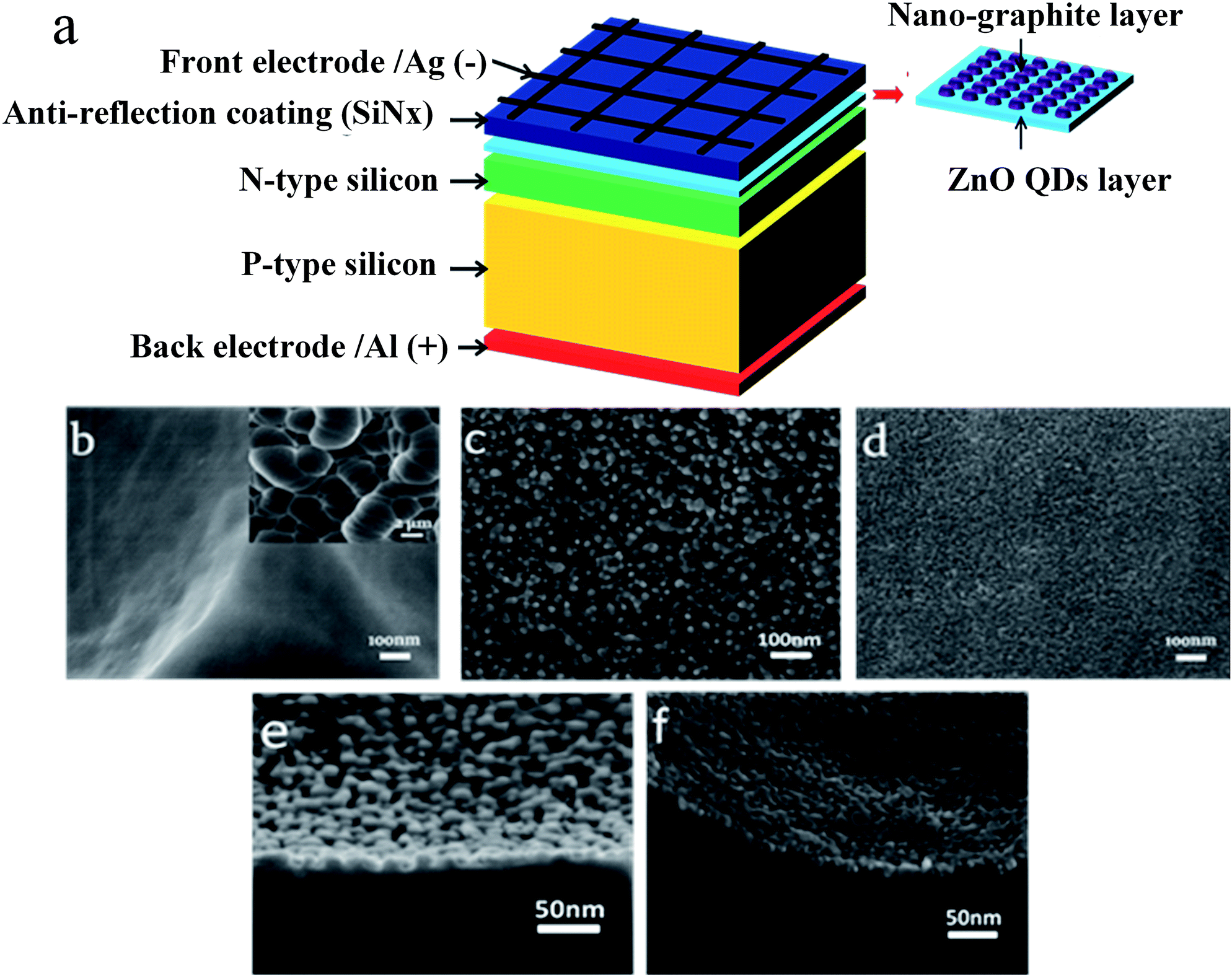 | ||
| Fig. 1 Schematics of the solar cell and the morphology of the c-Si wafer with ZnO QD and nano-graphite transport layers. (a) Schematic of the c-Si solar cell with ZnO QD and nano-graphite transport layers; (b) top-view FESEM images of the c-Si wafer; (c) top-view FESEM image of the c-Si wafer with a ZnO QD layer; (d) top-view FESEM image of the c-Si wafer with ZnO QD and nano-graphite transport layers; (e) cross-sectional view of the FESEM image of the c-Si wafer with a ZnO QD layer; and (f) cross-sectional view of the FESEM image of the c-Si wafer with ZnO QD and nano-graphite transport layers. | ||
So as to further analyse the size distribution of the ZnO QDs, TEM and HRTEM are utilized and more details of the sample preparation for TEM measurements are given in the ESI.† As shown in Fig. 2a, the diameter of the ZnO QDs is about 4 nm (XRD of ZnO in Fig. S2†). Fig. 2b shows the HRTEM image of ZnO QDs. The plane spacing of 0.289 nm for the ZnO (100) lattice plane is clearly observed. The selected area electron diffraction pattern of ZnO QDs (Fig. 2c) shows diffraction rings with a diameter of 7.14 (nm−1), which correspond well with the plane spacing of 0.280 nm in Fig. 2b.
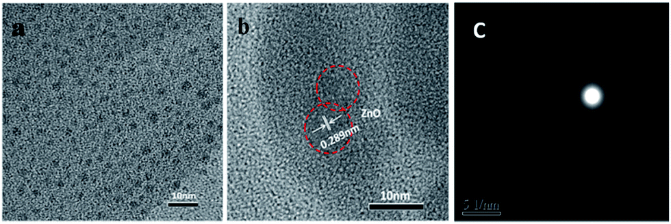 | ||
| Fig. 2 (a) TEM image of ZnO QDs powerfully sonicated from the surface of the c-Si wafer, (b) HRTEM image of ZnO QDs, and (c) selected area (electron) diffraction pattern of ZnO QDs. | ||
Because of the silicon energy band gap of 1.12 eV (300 K), the curves of the c-Si wafer absorption index have an abruptly raised shift at the wavelength of 1100 nm. Zinc oxide is a typical wide band gap semiconductor, whose energy gap is about 3.37 eV. The major absorption area of ZnO is the ultraviolet region. So, it can broaden the spectral response of crystalline silicon solar cells. Meanwhile, the nano-size effect of the ZnO QDs and nano-graphite offer the solar cells a nice light trapping, which enhances the absorption. Since graphite is a black material, it shows great absorption ability. In order to show the effects intuitively, we measured the absorption and reflectance using solar cells with SiNx anti-reflection. Fig. 3a and b show that the c-Si wafer has the lowest reflectance of 3.8%. Compared with the c-Si wafer, the reflectance of ZnO/Si and C–ZnO/Si solar cells is reduced obviously, in the full spectrum.
 | ||
| Fig. 3 The UV-Vis-NIR absorption and reflectance spectra of c-Si, ZnO/Si and C–ZnO/Si wafers in the range from 250 to 1250 nm. | ||
As we know, the electron affinity energy of silicon (XSi) is 4.05 eV and the electron affinity energy of zinc oxide (XZnO) is 4.5 eV. The energy gap of silicon {Eg(si)} is 1.12 eV, and the energy gap of ZnO is 3.37 eV. Therefore, the conduction-band offset (ΔEc) = XSi − XZnO = 4.05 − 4.5 = −0.45 eV and the valence-band offset (ΔEv) = (Eg ZnO − Eg Si) – (XSi − XZnO) = 3.37 − 1.12 − (−0.45) = 2.7 eV. Because the symbols of ΔEv and ΔEc are adverse, they typically belong to an n–n junction straddling gap type.25,26 As shown in Fig. 4, the depletion layer of electrons is the side of n-type ZnO, which forms a negative charge area, and the accumulation layer of electrons forming the positive charge area is the side of n-type Si. When the incident light irradiates the solar cells, photon-generated carriers are produced. The built-in electric field promotes the photon-generated electrons and the photon-generated holes to move towards opposite directions (photon-generated electrons move towards the ZnO layer and photon-generated holes move towards the Si layer), so as to accelerate the separation of electron–hole pairs.26,27 Thus, it can be seen that the minority carrier lifetime is inevitably prolonged.
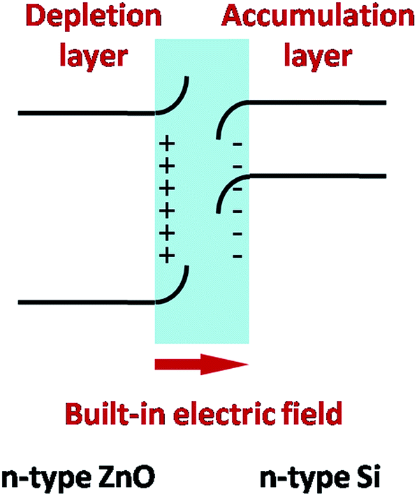 | ||
| Fig. 4 Schematic of the energy band diagram for an n–n typical junction belonging to a straddling gap type. | ||
The interactions between ZnO QDs, nano-graphite and Si were studied using X-ray photoelectron spectra, which were corrected by taking C 1s as a reference photoelectron peak located at 284.60 eV. Fig. 5a shows the XPS spectra of Zn 2p, which is composed of the characteristic peaks of Zn 2p1/2 and Zn 2p3/2. In ZnO/Si solar cells, the binding energies of Zn 2p1/2 and Zn 2p3/2 are 1045.4 eV and 1022.4 eV, respectively. When the solar cells contain the nano-graphite electron transport layer, the binding energies of Zn 2p1/2 and Zn 2p3/2 become 1045.1 eV and 1022.1 eV, respectively. The difference between both samples Zn 2p1/2 and Zn 2p3/2 is 23 eV, which is consistent with the reported ZnO.28Fig. 5b and c show the XPS spectra of Si 2p and Zn 2p3/2. The black lines are the standard data, red lines are the sample data of ZnO/Si solar cells and blue lines denote the sample data of solar cells with a nano-graphite electron transport layer. In the ZnO/Si solar cells, the binding energy of Si 2p reduces from 100.1 eV to 99.3 eV, while the binding energy of Zn 2p3/2 increases from 1021.5 eV to 1022.4 eV. As compared to the standard data, the binding energy of Zn 2p3/2 increases, while that of Si 2p reduces, which indicates that there exists a charge transfer between the ZnO QDs and n-type Si which confirms the formation of n–n junctions. Fig. 5d shows the XPS spectrum of C 1s peaks. The red line denotes the standard data of nano-graphite, which we purchased. It has a value of 284.9 eV. The black line is the curve of C 1s of solar cells, which contains the nano-graphite electron transport layer. The thumbnail shown in the top right corner is the XPS-peak-differentiation-imitating analysis for the black line. According to the two fit curves, there is abundant nano-graphite in the solar cells with its characteristic peaks at 284.8 eV except the reference photoelectron peak (C 1s) located at 284.60 eV. Besides the binding energy of nano-graphite decreases, the value of Zn 2p3/2 increases and the value of Si 2p decreases (Fig. 5b and c) implying that nano-graphite also has strong interactions with ZnO QDs and n-type Si. Thus, ZnO QDs, nano-graphite and c-Si have strong interaction and the charge exchanges demonstrate that there are good junctions in the designed C–ZnO/Si solar cell.
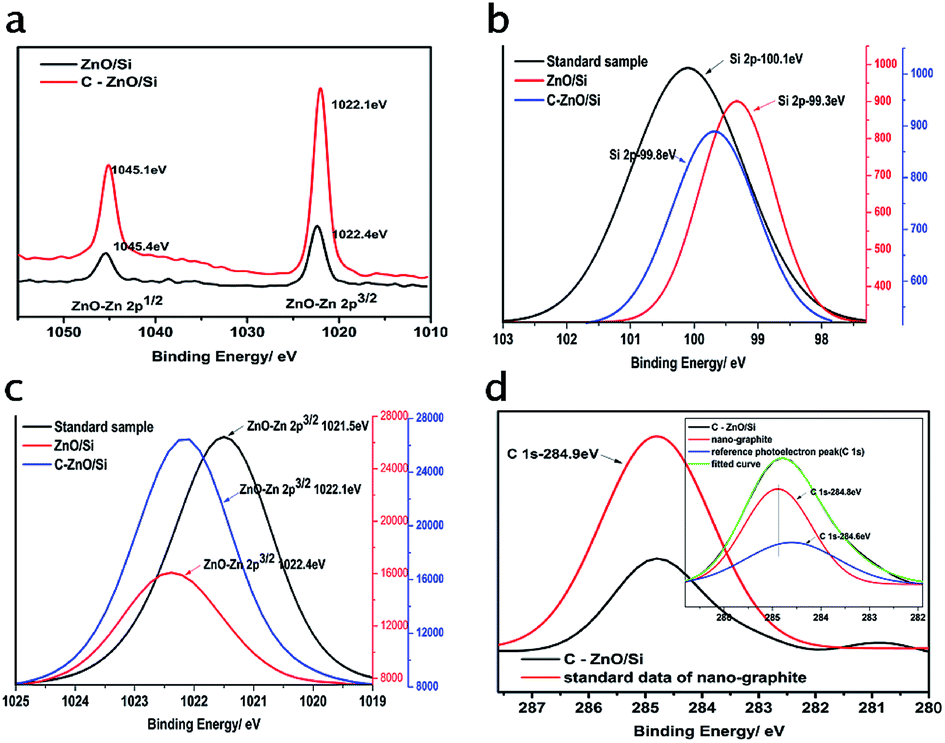 | ||
| Fig. 5 XPS spectra corrected by taking C 1s as a reference photoelectron peak located at 284.60 eV for (a) Zn 2p, (b) Si 2p, (c) Zn 2p3/2, and (d) C 1s peaks. | ||
In order to research the effects on carrier transport and analyse the roles of ZnO/Si n–n junctions and nano-graphite electron transport layers in solar cells, we use a Hall effect measurement system to evaluate the relevant parameters. The Hall mobility in this work is the electron mobility measured by the Hall effect. As shown in Fig. 6, the carrier density and Hall mobility of the c-Si wafer are 6.36 × 10¹⁶ (cm−3) and 30.41 (cm2 V−1 s−1), respectively. In ZnO/Si solar cells, because the oxygen vacancies are easily produced in the preparation of ZnO, the internal carriers of ZnO increase. So, the carrier density of solar cells improves, which is shown in Fig. 6. With the increasing carrier density, ionized impurity scattering and piezoelectric scattering which play great roles in electron mobility are shielded efficiently.29 Besides, the motion of electrons at the interface is quasi-two-dimensional (the direction of motion is parallel to the interface), which makes the scattering restrained. Because of the above two reasons the electron mobility is improved. In the graphite crystal, the carbon atoms in the same layer form covalent bonds via sp2 hybridization. Each carbon atom is covalently linked to three other atoms by three covalences. There is also a p-orbital remaining in each carbon atom. They overlap with each other and form π bonds, which have many electrons moving freely. So, the carrier density of C–ZnO/Si solar cells increases by 48% compared with the c-Si wafer. Apart from the above two reasons, the fact is that graphite is a conductor, and the electron mobility in nano-graphite is faster than in semi-conductors. So, we observed that the electron mobility in C–ZnO/Si solar cells obviously improved. Therefore, we believe that the nano-graphite electron transport layer can accelerate the transport of carriers.24–26
 | ||
| Fig. 6 The carrier density and Hall mobility of various solar cells. | ||
Fig. 7 shows the J–V curves of various solar cells under illumination with light of different wavelengths. They mainly verify the contribution value for power conversion efficiency under different wavelength areas.30 In ZnO/Si solar cells, in the range of 335 nm to 610 nm, the Jsc obviously increases, which is mainly attributed to the higher absorption and multiple exciton effects of QDs. However, only electron transportation actions of the nano-graphite layer in C–ZnO/Si solar cells have contribution to power conversion efficiency under illumination from 610 nm to 1800 nm. Thus, ZnO/Si show comparable performance with c-Si solar cells, and C–ZnO/Si solar cells have the highest power conversion efficiency of in range from 610 nm to 1800 nm.
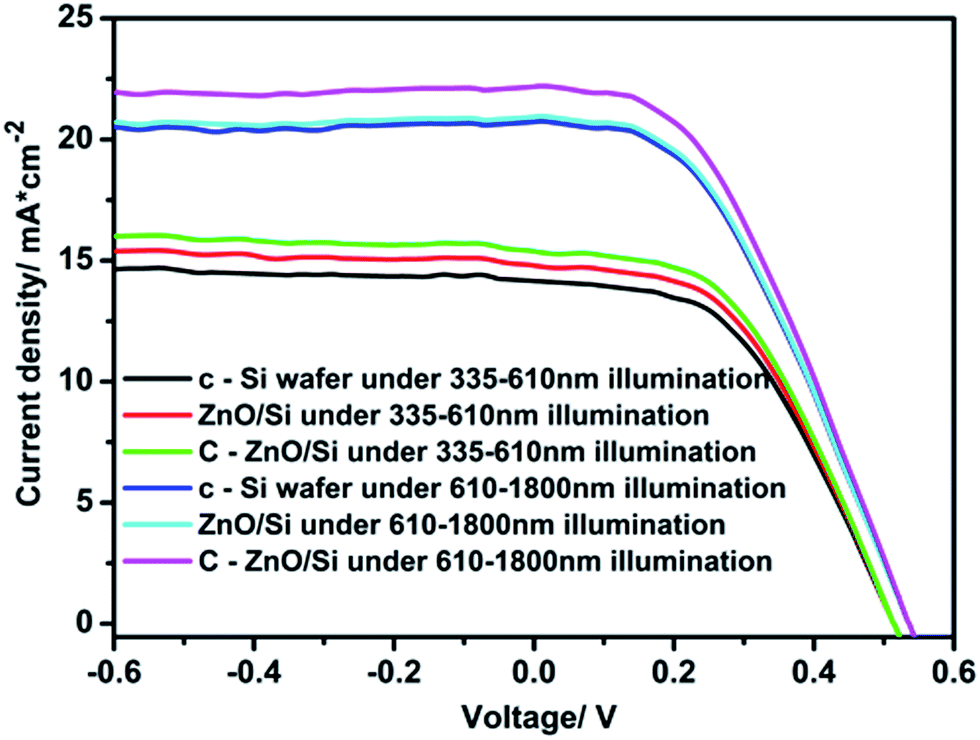 | ||
| Fig. 7 J–V curves of various solar cells under 335–610 nm illumination and 610–1800 nm illumination. | ||
Fig. 8 is the graph of the QE for various solar cells. As shown in this graph, we can observe that the QE increases within the scope of the full spectrum via using ZnO/Si n–n junctions and the nano-graphite electron transport layer. At the same time, the most important feature is that the QE increases in the wavelength range from 300 nm to 600 nm in particular, which is due to the use of the wide band gap ZnO QDs. ZnO QDs can enhance the absorption of the UV-light. Meanwhile, the quantum size effect and multiple exciton phenomenon increase the QE obviously. Around the wavelength of 900 nm, the QE improves, which illustrates that more high-energy photons are converted into electron–hole pairs due to the multiple exciton effects of QDs. Besides, because the diameter of graphite used in this study is less than 30 nm, the nano-graphite also shows nano-effects. For instance, surface effects make the nano-graphite have larger specific surface area; size effects enhance the light scattering on the surface of the c-Si wafer. All of this is good for the utilization of the incident light. Moreover, graphite shows high light absorption because it is a black material.21–24,31 Because of the presence of the high resistance semiconductor ZnO (Fig. S6†), the EQE of the solar cell can only reach nearly 95% (Fig. 8a). However, the internal quantum efficiency (IQE) of the C–ZnO/Si solar cell (Fig. 8b) exceeds the limit of 100% in the range of 300–400 nm, corresponding to the main absorption region of ZnO, which strongly supports the multiple exciton effects of QDs.
 | ||
| Fig. 8 Photovoltaic performances of various solar cells. (a) External quantum efficiency (EQE) of various solar cells. (b) Internal quantum efficiency (IQE) of various solar cells. (c) The minority carrier lifetime. (d) The J–V characteristics of different solar cells. | ||
Fig. 8c is the diagram of the minority carrier lifetime. It's relatively easy to find that ZnO/Si n–n junctions can enhance the performance of the solar cells. The primary reason is the built-in electric field. The Built-in electric field can promote the separation of electron–hole pairs and prolong the minority carrier lifetime. In the ZnO/Si solar cell with a nano-graphite electron transport layer, the performance of the solar cell further improves. Synergistic mechanisms of nano-graphite mainly include nano-effects and intrinsic optical properties demonstrated by Fig. 6. So, the nano-graphite electron transport layer enhances the light trapping and scattering, reduces the carrier recombination rate, and accelerates the transportation of electrons from heterojunctions to front electrodes. Fig. 8d shows the schematic of J–V characteristics of various solar cells, which are measured using an electrochemical workstation with a two-electrode configuration under 100 mW cm−2 illumination. Meanwhile, the C–ZnO/Si solar cell was measured under dark conditions in Fig. S7.† The detailed parameters are listed in Table 1. From Table 1, we can observe that all parameters of solar cells are improved to various extents. In the ZnO/Si solar cell formation, the short-circuit current density (Jsc) increases from 34.68 to 35.82 mA cm−2, compared with the reference one. The increase of short-circuit current density is because of the enhanced absorption of UV-light, quantum size effect, multiple exciton generation phenomenon in ZnO QDs and the built-in electric field in n–n junctions.21,31–33 The short-circuit current density further increases to 37.88 mA cm−2, when the nano-graphite is used as the electron transport layer. The main reasons are the nano-effect and the impacts of the electron transport layer. The nano-graphite electron transport layer separates the electron–hole pairs and collects more electrons to produce a larger photocurrent.21–24,31 The above-mentioned factors not only enhance the trapping of the solar spectrum but also improve the utilization rate. As we know, the open circuit voltage (Voc) is determined by the band gap of the semiconductor. The band gap of silicon is 1.12 eV, which determines the maximum theoretical open circuit voltage of 14 conventional c-Si solar cells to be 0.7 V. The conventional c-Si solar cells have a maximum theoretical open circuit voltage of 0.7 V for the band gap of 1.12 eV of silicon. Thus, we observe that the open circuit voltage increases from 0.54 V to 0.565 V. Another parameter of solar cells is the fill factor (FF). If the value of FF is closer to 100, then the series resistance will approach 0. The power conversion efficiency (PCE) is proportional to FF. All the above analyses are used to demonstrate the improvement of PCE. As is shown in Table 1, we can observe that the PCE of the ZnO/Si solar cell increases by 7.0% (from 12.73% to 13.62%), compared with the reference one. For the C–ZnO/Si solar cell, the PCE increases by 17.8% (from 12.73% to 14.99%).
| J sc (mA cm−2) | V oc (V) | FF (%) | η (%) | Δη (%) | |
|---|---|---|---|---|---|
| c-Si wafer | 34.68 | 0.54 | 67.98 | 12.73 | — |
| ZnO/Si | 35.82 | 0.565 | 67.30 | 13.62 | 7.0 |
| C–ZnO/Si | 37.88 | 0.565 | 70.07 | 14.99 | 17.8 |
Conclusions
ZnO QDs and nano-graphite were deposited on the surface of an n-type c-Si substrate through a simple solution phase deposition method and rapid annealing process. The ZnO QDs can not only broaden the range of spectral response and offer more electrons via multiple exciton effects but also facilitate the separation of photo-generated electron–hole pairs via forming n–n junctions with Si. Meanwhile, the nano-graphite can accelerate the electron collection and transportation from n-type Si to the front electrode. Thus, the designed Si solar cell with nano-graphite and ZnO QD layers shows improved power conversion efficiency of 14.99% compared with ZnO/c-Si (13.62%) and unmodified commercial c-Si (12.73%) solar cells.Experimental section
Materials
Polyvinyl pyrrolidone (PVP, K16–18, MW = 8000), zinc acetate dihydrate [Zn(CH3COO)2·2H2O], and ethanol 95% (C2H5OH 95%) are used. Nano-graphite (the diameter is 0–30 nm) is purchased from Nanjing Xianfeng nanomaterials technology co., LTD. Hydrofluoric acid (HF wt% = 40%) is purchased from Aladdin. Slices of c-Si wafers without Si3N4 purchased from Changzhou Yijing Optoelectronics Technology Co., Ltd. are applied in this work. The thickness of wafers is 200 μm with a bulk p–n junction.Fabrication of the sol–gel ZnO QDs
ZnO QDs are synthesized by using a solution of zinc acetate in ethanol (vol% = 95%). The concentrations of zinc acetate and PVP are 5 mmol L−1 and 6.7 g L−1, respectively. In order to gain a transparent and uniform sol, it is important that solution is stirred for about 30 min by magnetic stirring (300 rpm). Ultrasonic processing for 30 min is necessary in order to cut ZnO nanoparticles, so as to obtain ZnO QDs.Fabrication of the sol–gel ZnO QDs with a nano-graphite transport layer
Based on the fabrication of the sol–gel ZnO QDs, nano-graphite is added to the above sol. The concentration of the nano-graphite is 7 g L−1. After that, the solution is stirred by magnetic stirring (300 rpm). In order to ensure that the size of ZnO is less than 10 nm, ultrasonic processing for 30 min is needed again.Preparation of solar cells
The ZnO QD sensitization layer and nano-graphite transport layer are fabricated using a sol–gel dip coating technique to coat them on the surface of c-Si wafers. Firstly, the c-Si wafers are cleaned with hydrofluoric acid (wt% = 10%) for 150 s, and then the residual hydrofluoric acid and fluorosilicic acid are removed with redistilled water. Secondly, the cleaned substrates are dipped in the above two sols to coat ZnO QDs or ZnO QDs with the nano-graphite transport layer, respectively, with a dipping time of 30 s. Then, the c-Si wafers are rapidly transferred to a drying oven at 100 °C for 3 min at a heating rate of 20 °C min−1. Thirdly, with rapid thermal annealing in a muffle furnace at 900 °C for 5 min at a heating rate of 40 °C min−1, the ZnO/n-Si interface at the c-Si surface is formed. At the same time, the nano-graphite electron transport layer also forms a nice ohmic contact with the interface. Finally, c-Si wafers are conducted, via plasma etching, magnetron-sputtering Si3N4 and screen-printed electrodes.Characterization
A field emission scanning electron microscope (FESEM, Hitachi S-4800) and a high resolution transmission electron microscope (JEOL, JEM-2100) are used to observe the morphology and size distribution of the samples. The Hall mobility, carrier density and resistivity are measured using a model 7700A Hall measurement system. The minority carrier lifetime of the samples is measured using a Si wafer lifetime SEMILAB WT-2000 PVN. The current density–voltage (J–V) characteristics of the solar cells are measured using an electrochemical workstation (Zahner, Zennium) under 100 mW cm−2 illumination which is performed using a Class A AM 1.5 G spectral distributed Abet Technologies Sun 2000 Solar Simulator.Conflicts of interest
There are no conflicts to declare.Acknowledgements
This study is supported by the Program of National Natural Science Foundation of China (21501120), Open funds of the state key laboratory of rare earth resource utilization (RERU2016024), first-class discipline construction plan in Shanghai University, PCSIRT (IRT1269), Shanghai Science & Technology Committee (12521102501), and Shanghai Educational Committee (11ZR1426500, 14ZZ127).Notes and references
- Y. Xia, X. Pu, J. Liu, J. Liang, P. Liu, X. Li and X. Yu, J. Mater. Chem. A, 2014, 2, 6796–6800 CAS.
- D. M. Bagnall and M. Boreland, Energy Policy, 2008, 36, 4390–4396 CrossRef.
- W. Feng, Y. Wang, J. Liu and X. Yu, Chem. Phys. Lett., 2014, 608, 314–318 CrossRef CAS.
- R. T. Ross and A. J. Nozik, J. Appl. Phys., 1982, 53, 3813–3818 CrossRef CAS.
- M. A. Green, Solar Cells: Operating Principles, Technology And System Applications, University of New South Wales, 1982 Search PubMed.
- T. J. Kempa, R. W. Day, S. K. Kim, H. G. Park and C. M. Lieber, Energy Environ. Sci., 2013, 6, 719–733 CAS.
- Y. T. Yin, W. X. Que and C. H. Kam, J. Sol-Gel Sci. Technol., 2010, 53, 605–612 CrossRef CAS.
- F. Wang, D. Kozawa, Y. Miyauchi, K. Hiraoka, S. Mouri, Y. Ohno and K. Matsuda, Nat. Commun., 2015, 6, 6305 CrossRef CAS PubMed.
- L. Y. Chang, R. R. Lunt, P. R. Brown, V. Bulovi and M. G. Bawendi, Nano Lett., 2013, 13, 994 CrossRef CAS PubMed.
- S. Brittman, H. Gao, E. C. Garnett and P. Yang, Nano Lett., 2011, 11, 5189 CrossRef CAS PubMed.
- Z. Jia, Y. Zongfu, G. F. Burkhard, H. Ching-Mei, S. T. Connor, X. Yueqin, W. Qi, M. G. Michael, F. Shanhui and C. Yi, Nano Lett., 2009, 9, 279–282 CrossRef PubMed.
- H. Kobayashi, H. Mori, T. Ishida and Y. Nakato, J. Appl. Phys., 1995, 77, 1301–1307 CrossRef CAS.
- R. Pietruszka, B. S. Witkowski, S. Gieraltowska, P. Caban, L. Wachnicki, E. Zielony, K. Gwozdz, P. Bieganski, E. Placzek-Popko and M. Godlewski, Sol. Energy Mater. Sol. Cells, 2015, 143, 99–104 CrossRef CAS.
- R. Loef, A. J. Houtepen, E. Talgorn, J. Schoonman and A. Goossens, Nano Lett., 2009, 9, 856–859 CrossRef CAS PubMed.
- W. Feng, J. Liu, Y. Li, J. Liang and X. Yu, RSC Adv., 2014, 4, 14862–14867 RSC.
- A. J. Nozik, M. C. Beard, J. M. Luther, M. Law, R. J. Ellingson and J. C. Johnson, Chem. Rev., 2010, 110, 6873 CrossRef CAS PubMed.
- X. Pu, J. Liu, J. Liang, Y. Xia, W. Feng, Y. Wang and X. Yu, RSC Adv., 2014, 4, 23149–23154 RSC.
- S. Ameen, M. S. Akhtar, H. K. Seo, M. K. Nazeeruddin and H. S. Shin, J. Phys. Chem. C, 2015, 119, 150422051458005 Search PubMed.
- Y. Guo, G. L. Liu, H. X. Zhu, H. M. Yan, B. J. Zhu, S. Li, H. M. Yu, Y. J. Sun and G. H. Li, J. Synth. Cryst., 2014, 43, 1168–1173 CAS.
- M. Calik, F. Auras, L. M. Salonen, K. Bader, I. Grill, M. Handloser, D. D. Medina, M. Dogru, F. L, bermann and D. Trauner, J. Am. Chem. Soc., 2014, 136, 17802–17807 CrossRef CAS PubMed.
- Q. Wei, K. Hashimoto and K. Tajima, ACS Appl. Mater. Interfaces, 2011, 3, 139–142 CAS.
- J. Zhang, J. Tolentino, E. R. Smith, J. Zhang, M. C. Beard, A. J. Nozik, M. Law and J. C. Johnson, J. Phys. Chem. C, 2014, 118, 16228–16235 CAS.
- H. Arora, P. E. Malinowski, A. Chasin, D. Cheyns, S. Steudel, S. Schols and P. Heremans, Appl. Phys. Lett., 2015, 106, 40_41–426 CrossRef.
- E. Lim, T. Dai and M. Iwamoto, Appl. Phys. Lett., 2014, 105, 126–121 Search PubMed.
- S. Huang, Q. He, W. Chen, Q. Qiao, J. Zai and X. Qian, Chemistry, 2015, 21, 4085–4091 CrossRef CAS PubMed.
- M. Xu, T. Ye, F. Dai, J. Yang, J. Shen, Q. He, W. Chen, N. Liang, J. Zai and X. Qian, Chemsuschem, 2015, 8, 1218–1225 CrossRef CAS PubMed.
- O. Aina, M. Mattingly, F. Y. Juan and P. K. Bhattacharya, Appl. Phys. Lett., 1987, 50, 43–45 CrossRef CAS.
- J. F. Moulder, J. Chastain and R. C. King Jr, Chem. Phys. Lett., 1995, 220, 7–10 Search PubMed.
- T. Sahu and J. Patnaik, J. Appl. Phys., 2000, 88, 2658–2664 CrossRef CAS.
- X. M. Zhang, D. Golberg, Y. Bando and N. Fukata, Nanoscale, 2012, 4, 737–741 RSC.
- M. Calik, F. Auras, L. M. Salonen, K. Bader, I. Grill, M. Handloser, D. D. Medina, M. Dogru, F. Löbermann and D. Trauner, J. Am. Chem. Soc., 2014, 136, 17802–17807 CrossRef CAS PubMed.
- S. Huang, Q. He, W. Chen, Q. Qiao, J. Zai and X. Qian, Chemistry, 2015, 21, 4085 CrossRef CAS PubMed.
- M. Xu, T. Ye, F. Dai, J. Yang, J. Shen, Q. He, W. Chen, N. Liang, J. Zai and X. Qian, Chemsuschem, 2015, 8, 1218–1225 CrossRef CAS PubMed.
Footnote |
| † Electronic supplementary information (ESI) available. See DOI: 10.1039/c8se00007g |
| This journal is © The Royal Society of Chemistry 2018 |