
Fully functional semi-transparent perovskite solar cell fabricated in ambient air†
Stav
Rahmany
a,
Michael
Layani
ab,
Shlomo
Magdassi
a and
Lioz
Etgar
 *a
*a
aThe Hebrew University of Jerusalem, Institute of Chemistry, Casali Center for Applied Chemistry, Jerusalem 91904, Israel. E-mail: lioz.etgar@mail.huji.ac.il
bNanyang Technological University, School of Material Science and Engineering, 50 Nanyang Avenue, Singapore 639798
First published on 25th September 2017
Abstract
Organic–inorganic halide perovskite has excellent properties to function as light harvesters in solar cells due to the possibility to tune its optical properties and to use it as thin film absorber, at a few hundred-nanometer thicknesses. Herein, we demonstrate the fabrication of perovskite solar cells with controlled transparency, by the mesh assisted deposition process. Sequential fabrication of perovskite was performed in air, wherein a PbI2 grid was formed in the first step, and in the second step, the grid reacted selectively with methylammoniumiodide, resulting in a perovskite grid pattern. The best cells were obtained with a photoanode composed of mesoporous TiO2 with Al2O3 nanoparticles. The resulting semi-transparent perovskite solar cells, including a semi-transparent contact composed of MoO3/Au/MoO3 yielded a power conversion efficiency of 5.5% with an average transparency of 26% and efficiency of 8% for cells fabricated with a gold contact.
Introduction
Organic–inorganic halide perovskites are hybrid materials. This family of these materials enables the tuning of optical and electrical properties by changing either the organic or the inorganic component. In recent years, the organic–inorganic halide perovskite has demonstrated superior performance as a light harvester in solar cells, where its power conversion efficiency (PCE) increased to more than 22%.1 The use of organic–inorganic halide perovskite is not limited to a specific solar cell structure and it can be used in planar, mesoporous and hole conductor free configurations.2–5An interesting and important property of the perovskite is the possibility to make it transparent, thereby enabling fabrication of semi-transparent solar cells. There are several reports on semi-transparent perovskite solar cells, focusing on two main approaches. One is to make the perovskite layer as thin as possible in order to achieve the required transparency. However, the thin perovskite films absorb less light, thus impairing the performance.6 Moreover, thin perovskite films are usually made by evaporation technique, which is an expensive process.7,8 The second approach is related to fabrication of transparent electrical contacts. Guo et al. demonstrated the use of silver nanowires deposited from a solution in an inverted perovskite solar cell configuration.9 Laminated carbon nanotube films were also demonstrated as transparent electrode for perovskite solar cells, which permit dual side illumination of the solar cell.10 In addition, the graphene top-contact electrode was prepared by the chemical vapor deposition (CVD) method.11 Finally, the use of perovskite compositions using various cations show semi-transparent perovskite solar cells with 5.2% efficiency and 28% average visible transmittance (AVT).12 However, these results were obtained by fabricating a sandwich type material, which increases the complexity of fabrication and decreases the stability of the device. More recently, Bolink et al. have reported on a semi-transparent perovskite solar cell also employing a thin gold cathode, with 6.4% PCE and 29% full device AVT.7 However, this device was fabricated using thermal evaporation process of the perovskite material, which to date has some limitations for the industry.
Herein, we discuss a fully functional semi-transparent perovskite solar cell, based on a method in which the self-assembled perovskite precursor solution forms a transparent grid structure.13 The transparency of the perovskite grid could be tuned by controlling various parameters affecting the directed wetting process. The method is based on a fully wet deposition process, which takes only a few minutes and utilizes low cost screen-printing meshes.
Herein, we demonstrate the fabrication of semi-transparent perovskite solar cells composed of perovskite grids, with a photo anode composed of mesoporous TiO2 and Al2O3 nanoparticles, which was compared to the photoanode based solely on mesoporous TiO2 and showed better photovoltaic parameters. Furthermore, in this process the grid is formed in a two-step manner, thus enabling the higher density of perovskite. Using this approach, we were able to fabricate transparent solar cells with a power conversion efficiency of 5.5%, having more than 26% transparency for the full cells. We investigated the parameters affecting the grid formation such as precursor concentration, wetting agent concentration and the annealing while forming the grid. It was found that the best grid formation can be obtained at annealing to 70 °C during the self-assembly process. Furthermore, the best AVT and power conversion efficiency values were obtained while using a mesh having an opening of 85 μm.
Results and discussion
The semi-transparent perovskite solar cells herein are fabricated by a two-step deposition process, which is performed at 70 °C and ambient humidity, using a simple, low cost mesh-assisted assembly deposition method (Fig. 1). The first step is the formation of PbI2 in a grid pattern. The induced wetting of the PbI2 solution along the walls of the screen printing mesh is due to the heating of the mesh during fabrication. The alignment results in formation of a grid with controllable openings, as shown in the Ultra-High Resolution Scanning Electron Microscopy (UHRSEM) images in Fig. 2B and 2E while using screen meshes having opening of 85 μm and ∼200 μm, respectively. | ||
| Fig. 1 Schematic of the semi-transparent perovskite solar cell made by a two step deposition process. In the first step, the PbI2 grid is formed and annealed, and then the entire electrode is dipped into the MAI solution forming the MAPbI3 grid. In the final stage, dielectric–metal–dielectric (DMD) contact is evaporated on top of the hole transport material (HTM) layer. | ||
 | ||
| Fig. 2 HRSEM images for 0.2 M PbI2 grid obtained using: (A) 85 μm mesh size without annealing. (B) 85 μm mesh size with annealing. (C) Chemical mapping for PbI2 (Pb in yellow color and in the inset I is in red color) grid formed during annealing using 85 μm mesh size. (D) 240 μm mesh size without annealing. (E) 240 μm mesh size with annealing. (F) Chemical mapping for PbI2 (Pb in yellow color and in the inset, I is in red color) grid formed during heating using 240 μm mesh size. The temperature during the grid formation was ∼70 °C for samples B, C, E and F. | ||
Patterning of perovskite crystals is not widely reported and is typically performed by a subtraction (top down) process. Herein, we demonstrate a unique induced self-assembly process in which the grid formation is easily achieved in a bottom-up approach. The process is performed using low concentrations of PbI2, and during annealing the PbI2 grid formation is induced. In order to study the effect of annealing on the grid formation, we compared the grid fabricated via annealing during the self-assembly process with the grid fabricated at ambient temperature. Without annealing, the PbI2 does not self-assemble and there is no grid formation, as can be seen in Fig. 2A and D. The annealing of the substrate during grid formation, which was not performed in the previously reported method,13 induces island formation before the assembling of particles along the wires of the mesh.
In a typical self-assembly process under ambient conditions, molecules assemble first within the junctions, followed by the wires of the mesh during the slow evaporation of the solvent. The annealing induces the flow of the liquid towards the edges due to the decrease in viscosity. Furthermore, annealing induces crystallization of PbI2. Without annealing, the rate of crystallization is slow, inducing lateral crystallization that prevents the flow of the liquid and molecules along the mesh wires. It should be noted that at higher concentration of PbI2 of more than 0.6 M, the grid is completely connected as can be seen in Fig. 2S.† This is in contrast to a typical grid assembly process,14 wherein the grid is formed more slowly at ambient temperature resulting in formation of lines and junctions simultaneously. In order to assess whether the grid formed during annealing is composed of PbI2, chemical mapping using energy dispersive spectroscopy (EDS) was applied. The mapping was done for Ti (presented in blue color), Pb (yellow color) and I (red color). As can be seen in Fig. 2C and F, the grid is composed solely of PbI2. Following the formation of the PbI2 grid, the substrate with the PbI2 grid was dipped in methyl ammonium iodine (MAI) solution. MAI reacted with PbI2 forming a grid of MAPbI3. It should be noted that there is almost no MAPbI3 residue between the PbI2 grid lines (Fig. 2B, E and 5S† and EDX measurement shown in Table 3S†), thus enabling the semi-transparent structures. Fig. 3SC† shows a cross section high resolution scanning electron microscopy (HR-SEM) image of the mesoporous TiO2 + Al2O3 NPs film, in which the Al2O3 NPs are intercalated within the mesoporous TiO2 film. When comparing the PbI2 grid formation deposited on the meso TiO2 + Al2O3 NPs to meso TiO2, similar grid geometry is obtained as seen in Fig. 3SA and B,† respectively. However, the transparency of the resulting perovskite grid for TiO2 + Al2O3 was found to be lower compared to that of the grid fabricated on mesoporous TiO2 film, as shown in Fig. 3SD.† In general, there are three parameters that dictate the way the self-assembly occurs: (1) wetting, which creates a flux during evaporation and takes the particles to the periphery in case of a drying droplet. (2) Capillary forces that make the particles assemble along the wires of the mesh. (3) The chemical\physical interaction of the dispersed particles/molecules with the surface. In order to qualitatively assess these parameters, 100 μL droplets of PbI2 were placed on the two type of substrates (without a mesh) and the rims of the droplet that are formed during drying due to the coffee stain effect15,16 were imaged by an optical microscope (Fig. 4S†). It appears that in the case of TiO2 surface, the particles favor the adhesion to the surface (thus a thinner line is formed in the drying droplet) and the flux and capillary forces are less strong. Therefore, more particles stay at the center of the grid forming less concentrated grid lines (Fig. 4SB†). In the case of TiO2 + Al2O3, the flux and capillary forces are much stronger than the adhesion to the substrate, and thus a majority of the particles move towards the periphery and form a thick line of the drying droplet as shown in the optical microscopy image at Fig. 4SA.†
We compared the photovoltaic (PV) performance of the semi-transparent solar cells of the structures: FTO glass/blocking layer/mesoTiO2/MAPbI3 grid/spiro/Au and FTO glass/blocking layer/meso TiO2 + Al2O3 NPs/MAPbI3 grid/spiro/Au. It was found that cells having meso TiO2 + Al2O3 NPs as the photoanode perform better than the cells with only meso TiO2 NPs as the photoanode. The average PCE for the cells based on meso TiO2 only is, 1.8% ± 0.1 with an average visible transparency (AVT) of 34% ± 0.5, which is significantly lower than the average PCE obtained for TiO2 + Al2O3 NPs case as is discussed below. The PV parameters of both type of cells (i.e. meso TiO2 and TiO2 + Al2O3) can be seen in Tables S1, S2 and 4S.†
Numata et al.17 reported similar results in which composite of TiO2 and Al2O3 NPs perform better as the photoanode than meso TiO2 only. This is due to a change in the electron transport path while using insulating Al2O3 NPs and n-type semiconducting TiO2 NPs in the same photoanode. Similar observations were reported by Min Cha et al.18 in which better PV performance was observed for 25% Al2O3 NPs in the meso TiO2 photoanode. Due to the better PV performance in the case of photoanode based on meso TiO2 + Al2O3 NPs, we decided to continue the experiments with cells made of photoanodes based on meso TiO2 + Al2O3 NPs.
One of the key parameters affecting the transparency of the cell, and thus its efficiency, is the PbI2 concentration. The resulting AVT and PV parameters for different PbI2 concentrations and different mesh sizes (85 and 240 μm) are presented in Tables 1 and 2 correspondingly. The different densities of the perovskite grid affect the transparency of the cells mainly at a high concentration of PbI2.
| V oc (V) | J sc (mA cm−2) | Fill factor | Efficiency (%) | PbI2 concentration (M) | AVT (%) |
|---|---|---|---|---|---|
| 0.71 (0.7 ± 0.01) | 10.7 (8.85 ± 1.3) | 61 (61 ± 4.7) | 4.65 (3.8 ± 0.45) | 0.1 | 28 (27.6 ± 3.3) |
| 0.7 (0.7 ± 0.01) | 10.8 (9.6 ± 1.2) | 63 (58.6 ± 3.3) | 4.7 (3.9 ± 0.6) | 0.15 | 25 (25 ± 0.1) |
| 0.85 (0.74 ± 0.05) | 13.1 (11.1 ± 1.6) | 72 (65.3 ± 6.3) | 8 (5.4 ± 1.3) | 0.2 | 14.5 (18.9 ± 4.3) |
| 0.77 (0.8 ± 0.01) | 11.8 (9.7 ± 1) | 62.5 (66.8 ± 2.6) | 5.7 (5.2 ± 0.4) | 0.5 | 11 (10.23 ± 0.1) |
| 0.83 (0.68 ± 0.25) | 8.5 (9.2 ± 1) | 65.5 (59 ± 12.5) | 4.65 (3.8 ± 1.6) | 0.7 | 8 (8.2 ± 1.6) |
| 0.78 (0.78 ± 0.04) | 5.3 (7.4 ± 2.15) | 52 (57.9 ± 8.55) | 2.22 (3.5 ± 1.1) | 1 | 6 (6.55 ± 0.35) |
| V oc (V) | J sc (mA cm−2) | Fill factor | Efficiency (%) | PbI2 concentration (M) | AVT (%) |
|---|---|---|---|---|---|
| 0.77 (0.66 ± 0.16) | 9.7 (7.7 ± 2.2) | 59 (55.6 ± 7.8) | 4.4 (3 ± 1.3) | 0.1 | 29 (26.45 ± 2.6) |
| 0.75 (0.74 ± 0.01) | 10.2 (9.4 ± 1) | 60 (59 ± 4.4) | 4.6 (4.2 ± 0.7) | 0.15 | 24 (23.7 ± 2.3) |
| 0.76 (0.77 ± 0.02) | 12.8 (12.8 ± 1.4) | 69.5 (62.3 ± 4.9) | 6.7 (6.1 ± 0.6) | 0.2 | 20.5 (21.75 ± 1.4) |
| 0.79 (0.67 ± 0.23) | 10.7 (9.6 ± 0.9) | 45 (48.2 ± 8.4) | 3.8 (3.2 ± 1.15) | 0.5 | 16 (14.2 ± 1.6) |
| 0.78 (0.76 ± 0.05) | 6.2 (7 ± 2.9) | 61 (56 ± 10) | 3 (3.2 ± 1.5) | 0.7 | 12 (9.7 ± 4) |
| 0.81 (0.75 ± 0.06) | 5.4 (4.7 ± 3.2) | 64 (49.5 ± 11.3) | 2.8 (1.8 ± 1.1) | 1 | 9 (8.9 ± 1.5) |
The corresponding current voltage (JV) curves for the grids obtained by 85 and 240 μm open mesh size are presented in Fig. 3A and B, respectively. It was found that the PV parameters and the AVT change while varying the PbI2 concentration. As shown in Fig. 3C, at high concentration of PbI2 (>0.2 M) the transparency is higher for the 240 μm mesh compared to the 85 μm mesh, while at low concentrations of PbI2 (<0.2 M) there is almost no difference in the transparency. This supports the difference in the PV performance for the 85 μm mesh size, which is higher than that of the 240 μm mesh size.
 | ||
| Fig. 3 JV curves for the semi-transparent solar cells fabricated using different PbI2 concentrations (M). (A) 85 μm mesh size. (B) 240 μm mesh size. (C) AVT as a function of the PbI2 concentration in the grid formation. (D) XRD spectra of MAPbI3 grid fabricated using two different PbI2 concentrations 0.1 M and 1 M. | ||
Interesting aspect to be considered in the case of semi-transparent solar cells is their real active area. The real active area is determined as the area that is covered by the perovskite, i.e. the grid lines, and it is obvious that it is smaller than the whole active area of the cell. The PCE of the real active area (the calculation is given in the ESI†) is 10.4% and 11.5% for 85 μm and 240 μm, respectively.
Fig. 3D shows the XRD spectra of the MAPbI3 perovskite grid formed from low PbI2 concentration (0.1 M) compared to high PbI2 concentration (1 M). As can be seen, in the case of the MAPbI3 formed from low PbI2 concentration, no residues of PbI2 are found, unlike the MAPbI3 formed from 1 M PbI2 where residues of PbI2 are found. This is the main reason that at low concentration of PbI2, a better PV performance can be achieved for both mesh opening sizes. This is due to the fact that at high concentration of PbI2, the PbI2 grid is not fully converted to MAPbI3. Therefore, the best overall performing cells are fabricated using 0.2 M PbI2 even though at high PbI2 concentration, the transparency decreases, which might suggest a better PV performance.
Additional parameters that may affect the grid formation are the MAI concentration in the dipping solution and the wetting agent (WA) concentration. Usually, increasing the concentration of the wetting agent lowers the surface tension, thus resulting in better wetting which should improve the grid formation. However, at high concentration of the WA, there is an increase in the organic molecule residues, which results in a lower PV performance. The effect of the WA concentration on the PV performance is presented in Table 1S:† high concentration results in low efficiency while the transparency is not affected. Table 2S† shows the change in the MAI concentration where the WA and PbI2 concentrations are kept constant (mesh size 85 μm). As can be observed, 0.063 M of MAI results in the best PV performance.
Fig. 4 presents the change in the PV parameters (open circuit voltage-Voc and power conversion efficiency) as a function of the PbI2 concentration. As previously discussed, the best PV parameters are observed at 0.2 M of PbI2 for both the mesh sizes of 85 and 240 μm, with power conversion efficiency of 8% and 6.7% at 14.5% and 20% transparency, respectively. The forward and reverse scans of the best performing semi-transparent cells can be observed in Fig. 4C and D for 85 and 240 μm, respectively. In both cases, the hysteresis is small. However, for concentrations lower and higher than 0.2 M, the hysteresis is more pronounced (Fig. 1S†). The reason for that is unclear yet and further study is required.
 | ||
| Fig. 4 Open circuit voltage (Voc) and efficiency as a function of PbI2 concentration. (A) 85 μm mesh size and (B) 240 μm mesh size. JV curves forward and reverse scan for (C) 85 μm mesh cell and (D) 240 μm mesh cell. | ||
Next, for obtaining a complete semi-transparent solar cell, a semi-transparent electrical contact was fabricated. Therefore, the typically used gold contact was replaced by a dielectric–metal–dielectric (DMD) back contact composition.19 The semi-transparent contact is composed of a thin Au layer sandwiched between MoO3 thin films with bottom MoO3 (B-MoO3) and top MoO3 film (T-MoO3). Fig. 5B shows a photograph of the complete semi-transparent perovskite solar cell. As can be seen visually, the entire cell has high transparency showing its applicability in the field of construction of integrated photovoltaics (BIPV). In order to find the best composition of the semi-transparent contact, various thicknesses of B-MoO3 and Au films were evaluated, while keeping the T-MoO3 thickness constant (35 nm).
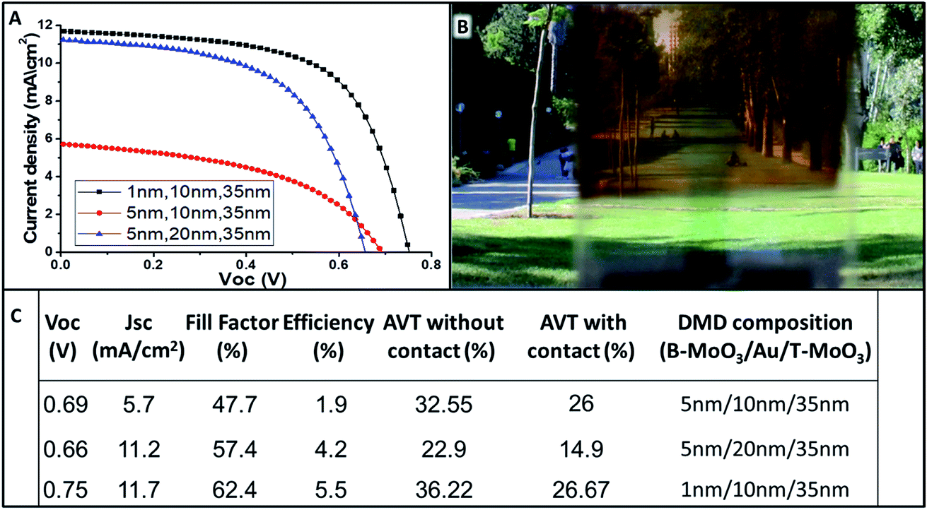 | ||
| Fig. 5 (A) JV curves of the semi-transparent perovskite solar cells with different Dielectric–Metal–Dielectric (DMD) contact composition. (B) Photograph of the complete solar cell and how an object can be viewed through the cell. (C) PV parameters of the semi-transparent perovskite solar cells with the semi-transparent contact. The results are for cells fabricated using 0.2 M PbI2 with 85 μm mesh size. | ||
Fig. 5A and C summarize the PV parameters and JV curves for the various thicknesses studied. The best semi-transparent contact composition was observed for 1 nm/10 nm/35 nm (B-MoO3/Au/T-MoO3). The reduction in transparency due to the B-MoO3 contact is acceptable, having an AVT of 26.6% with a PCE of 5.5% for a complete semi-transparent perovskite solar cell.
Fig. 6 shows a literature comparison of the leading results obtained for semi-transparent perovskite solar cells composed by wet deposition methods. The arrow in the figure indicates the aim while developing semi-transparent solar cells, i.e. high transparency with high efficiency. Minimal average visible transparency for building applications is at least 20%.
 | ||
| Fig. 6 A plot of leading published results of semi-transparent solar cells fabricated by wet deposition method12,13,20,21 (* indicates grid using 240 μm, # indicates semi-transparent full device). | ||
As can be seen in the plot in Fig. 6, the best PV performance obtained for a process based on a simple, low-cost wet deposition process is by the use of the approach presented herein.
Conclusions
Herein, we have demonstrated the fabrication of semi-transparent, highly efficient perovskite solar cells, by combining a directed self-assembly method with a sequential deposition technique to form a controlled perovskite grid under ambient conditions and low temperature. PbI2 grids were formed using two different mesh opening sizes, 85 and 240 μm, which enabled the achievement of controlled transparency. Dipping the resulting PbI2 grid in a solution of methylammoniumiodide converted the PbI2 grid into high quality perovskite grid, resulting in a high PV performance. In addition, Al2O3 NPs, which were embedded within the mesoporous TiO2 layer, also improved the cell performance. Finally, we successfully fabricated a semi-transparent electrical contact on the semi-transparent perovskite solar cell demonstrating 5.5% efficiency with 26% AVT. These findings can open the possibility for efficient low cost solar windows for building integrated PV (BIPV).Experimental
Substrate preparation
A conducting glass coated with FTO (SnO2) (15 Ω cm−1, Pilkington) was etched with Zn powder and HCl (37%) to create an electrode pattern. The FTO glass was cleaned with acetone and water and then sonicated for 15 min with ethanol, acetone and deionized water. Finally, the patterned glass was exposed to oxygen plasma treatment for 5 min. A compact TiO2 layer was deposited by a spin-coater (2000 rpm for 1 min) using a solution that contained titanium diisopropoxidebis (TiDIP, 75% isopropanol, Aldrich) in ethanol. The coated glass was annealed on a 450 °C hot plat for 30 min. A mesoporous TiO2 layer was formed by spin coating (2000 rpm for 30 s) using a solution of titania paste (20 nm, Dyesol) diluted in ethanol 4 times by weight ratio (0.2 g titania paste in 0.64 g ethanol) and annealed at 500 °C for 30 min. Next, an Al2O3 nano-particles solution, diluted 16 times in isopropanol by weight (0.1 g Al2O3 in 1.6 g isopropanol), was dropped on top of the TiO2 mesoporous layer and was spin coated for 30 s at 6000 rpm, followed by annealing at 500 °C for 30 min. Finally, the electrodes were soaked in 2 M aqueous TiCl4 solution at 70 °C and annealed at 500 °C for 30 min.Perovskite grid deposition
For deposition, solutions of PbI2 (Sigma-Aldrich 98%) in N-dimethylformamide (DMF) were used (1 M, 0.7 M, 0.5 M, 0.2 M, 0.15 M, 0.1 M) with added surfactant (BYK333) (1 wt% from a 10 wt% solution in DMF). The electrodes were placed on a hot plate (55 °C). On top of them, a polymer mesh (240 or 85 μm opening size) was placed in order to form the pattern. After 2 min, 7 μL from the PbI2 solution were dropped on the electrode, and 20 min later the mesh was removed and the electrodes were annealed for 30 min at 70 °C. Finally the electrodes were dipped in 0.063 M MAI (CH3NH3I) solution (0.1 g in 10 mL isopropanol) for 30 s and annealed for 30 min at 90 °C.A hole transporting material (HTM) solution was made by dissolving 0.036 g of 2,2′,7,7′-tetrakis-(N,N-di-4-methoxyphenylamino)-9,9′-spirofluorine (spiro-OMeTAD) in 500 μL chlorobenzene. To this solution, a 13.3 μL of bis(trifluoromethane)sulfonimide lithium salt in acetonitrile (520 mg mL−1), 14.5 μL of tris(2-(1H-pyrazol-1-yl)-4-tert-butylpyridine)-cobalt(III) tris(bis(trifluoromethylsulfonyl)imide) in acetonitrile (300 mg mL−1) and 9.6 μL of 4-tert-butilpyridine were added to create the final HTM solution. Furthermore, 40 μL of the spiro solution was dropped with a waiting time of 30 s and was then spin coated at 3000 rpm for 30 s. In addition, 70 nm layer of gold was evaporated under pressure of 5 × 10⁻⁶ Torr at a rate of 1.1 A s−1 to create the back contact.
DMD electrode
The bottom layer of MoO3 and the Au layer on top of it were thermally evaporated at a rate of 0.1 A s−1 up to the desired thickness. The top layer of MoO3 was evaporated at a rate of 0.3 A s−1 up to 35 nm, forming the semi-transparent contact. The thickness was defined by varying the exposure time in the thermal evaporator.PV characterization
The measurements of the photovoltaic parameters were made using a New Port system, an Oriel I–V test station and Oriel Sol3A simulator. Class AAA solar simulator was used for spectral performance, uniformity of irradiance and temporal stability. The device contained a 450 W xenon lamp, and the output power was adjusted to match AM1.5 global sunlight (100 mW cm−2), as the spectral match classification were IEC60904-9 2007, JIC C 8912, and ASTM E927-05. I–V curves were extracted by applying an external bias to the cell and measuring the generated photocurrent with a Keithley model 2400 digital source meter. The voltage stop was 10 mV and the delay time was 5 ms. The measurements were made using a mask with an aperture area of 0.04 cm2.AVT measurements
The UV-vis measurements were recorded using a Jasco V-670 spectrophotometer. A substrate cell was used as a reference for the transparency measurements, while the measured cell contained all the layers except spiro-OMeTAD and gold. The average transmittance was calculated in the ranges of 400–800 nm wavelength.Morphological characterization
In order to observe the grid pattern, optical microscopy picture has been captured (MRC Israel). Additionally, an Ultra-High Resolution Scanning Electron Microscopy (UHR-SEM) was performed using Magellan UHR-SEM of FEI (Field Emission Instruments, The Netherlands) at a condition of 5 kV at various magnifications.XRD measurements
X-ray powder diffraction measurements were performed on the D8 Advance diffractometer (Bruker AXS, Karlsruhe, Germany) with a secondary graphite monochromator, 2° Sollers slits and 0.2 mm receiving slit. XRD patterns within the range from 5° to 75° 2θ were recorded at room temperature using CuKα radiation (λ = 1.5418 Å) with the following measurement conditions: tube voltage of 40 kV, tube current of 40 mA, step-scan mode with a step size of 0.02° 2θ and counting time of 1 s per step.EDS measurement
EDS was performed on samples that contain FTO/compact TiO2/m.p TiO2 + Al2O3/PbI2 grid using ESEM Quanta200 (FEI company).Conflicts of interest
The authors declare no conflicts of interest.Acknowledgements
We would like to thank the support by the Israel ministry of science and technology and the Singapore Research Foundation under the Campus for Research and Technological Enterprise (CREATE): NTU-HUJ Nanomaterials for energy and energy-water nexus program.References
- http://www.nrel.gov/pv/assets/images/efficiency_chart.jpg .
- M. Lee, J. Teuscher, T. Miyasaka, T. N. Murakami and H. J. Snaith, Science, 2012, 338, 643–646 CrossRef CAS PubMed.
- L. Etgar, P. Gao, Z. Xue, Q. Peng, A. K. Chandiran, B. Liu, M. K. Nazeeruddin and M. Graetzel, J. Am. Chem. Soc., 2012, 134, 17396 CrossRef CAS PubMed.
- H. S. Kim, C. R. Lee, J. H. Im, K. B. Lee, T. Moehl, A. Marchioro, S. J. Moon, R. Humphry-Baker, J. H. Yum, J. E. Moser, M. Gratzel and N. G. Park, Sci. Rep., 2012, 2, 591 CrossRef PubMed.
- S. Aharon, S. Gamliel, B. El Cohen and L. Etgar, Phys. Chem. Chem. Phys., 2014, 16, 10512–10518 RSC.
- G. E. Eperon, V. M. Burlakov, A. Goriely and H. J. Snaith, ACS Nano, 2014, 8(1), 591–598 CrossRef CAS PubMed.
- C. Roldán-Carmona, O. Malinkiewicz, R. Betancur, G. Longo, C. Momblona, F. Jaramillo, L. Camachob and H. J. Bolink, Energy Environ. Sci., 2014, 7, 2968–2973 Search PubMed.
- E. D. Gasper, Y. Peng, Q. Houb, L. Spiccia, U. Bach, J. J. Jasieniak and Yi-B. Cheng, Nano Energy, 2015, 13, 249–257 CrossRef.
- F. Guo, H. Azimi, Y. Hou, T. Przybilla, M. Hu, C. Bronnbauer, S. Langner, E. Spiecker, K. Forbericha and C. J. Brabec, Nanoscale, 2015, 7, 1642–1649 RSC.
- Z. Li, S. A. Kulkarni, P. P. Boix, E. Shi, A. Cao, K. Fu, S. K. Batabyal, J. Zhang, Q. Xiong, L. Helena Wong, N. Mathews and S. G. Mhaisalkar, ACS Nano, 2014, 8(7), 6797–6804 CrossRef CAS PubMed.
- P. You, Z. Liu, Q. Tai, S. Liu and F. Yan, Adv. Mater., 2015, 27, 3632–3638 CrossRef CAS PubMed.
- G. E. Eperon, D. Bryant, J. Troughton, S. D. Stranks, M. B. Johnston, T. Watson, D. A. Worsley and H. J. Snaith, J. Phys. Chem. Lett., 2015, 6, 129–138 CrossRef CAS PubMed.
- S. Aharon, M. Layani, B.-E. Cohen, E. Shukrun, S. Magdassi and L. Etgar, Adv. Mater. Interfaces, 2015, 2, 1500118 CrossRef.
- M. Layani and S. Magdassi, J. Mater. Chem., 2011, 21(39), 15378–15382 RSC.
- L. Michael, M. Gruchko, O. Milo, I. Balberg, D. Azulay and S. Magdassi, ACS Nano, 2009, 3(11), 3537–3542 CrossRef PubMed.
- R. D. Deegan, O. Bakajin, T. F. Dupont, G. Huber, S. R. Nagel and T. A. Witten, Nature, 1997, 389(6653), 827–829 CrossRef CAS.
- Y. Numata, Y. Sanehira and T. Miyasaka, ACS Appl. Mater. Interfaces, 2016, 8, 4608–4615 CAS.
- J.-M. Cha, J.-W. Lee, D.-Y. Son, H.-S. Kim, I.-H. Jang and N.-G. Park, Nanoscale, 2016, 8, 6341–6351 RSC.
- E. D. Gasperaa, Y. Peng, Q. Hou, L. Spiccia, U. Bacha, J. J. Jasieniak and Y.-B. Cheng, Nano Energy, 2015, 13, 249–257 CrossRef.
- S. Chen, B. Chen, X. Gao, B. Dong, H. Hu, K. Yan, W. Wena and D. Zou, Sustainable Energy Fuels, 2017, 1, 1034–1040 CAS.
- G. E. Eperon, V. M. Burlakov, A. Goriely and H. J. Snaith, ACS Nano, 2014, 8(1), 591–598 CrossRef CAS PubMed.
Footnote |
| † Electronic supplementary information (ESI) available. See DOI: 10.1039/c7se00383h |
| This journal is © The Royal Society of Chemistry 2017 |