DOI:
10.1039/C7RA09135D
(Paper)
RSC Adv., 2017,
7, 45280-45286
Three-dimensional graphene networks and reduced graphene oxide nanosheets co-modified dye-sensitized solar cells†
Received
18th August 2017
, Accepted 13th September 2017
First published on 22nd September 2017
Abstract
Graphene assisted dye-sensitized solar cells (DSSCs) have drawn increasing attention because of their high performances. However, two bottlenecks (the high defect density and the discontinuous structure) of the widely adopted reduced graphene oxide (RGO) nanosheets bring about that the practical photovoltaic properties are far inferior to the theoretical prediction values. Therefore, three-dimensional graphene networks (3DGNs) of high quality have been employed to modify DSSCs to avoid the above mentioned problems. However, a close contact between the graphene basal plane and TiO2 particles in the resulting photoanode is difficult to achieve due to the absence of surface functional groups of the 3DNG. In this study, the RGO nanosheets and 3DGNs co-modified DSSCs are prepared, and the advantages from these two modifiers can give full play to their synergy. The added RGO nanosheets enhance the electron transport ability at the interfaces between graphene, TiO2 and conductive substrate. After optimizing the reduction degree and mass fraction of the RGO nanosheets, the power conversion efficiency of the resulting DSSC reaches 7.68%, which is much higher than those cases of using the 3DGNs (or RGO nanosheets) as modifier alone.
Introduction
Graphene modified dye sensitized solar cells (DSSCs) have attracted increasing attention because of their high photovoltaic performances.1–6 The large BET area and the high electron mobility of graphene in theory cause it to be a promising modifier to enhance the photovoltaic performance of the resulting photoanode and resulting devices. Gao et al. reported that the power conversion efficiency (η) increases from 2.69% to 4.28% after adding 0.5 wt% reduced graphene oxide (RGO) nanosheets.6 Chen et al. adopted RGO nanosheets (1 wt%) to enhance the electron transport ability of the photoanode, and the η improves to 6.86% (15% higher than that of the pure TiO2 photoanode).7 Chen's group fabricated a sandwich-structured TiO2/graphene nanosheets electrode for the DSSCs, which brings about a 60% improvement in η (reaches 3.93%).8 Moreover, a photoanode with a novel three-layer construction based on the RGO and TiO2 has been proposed by our group, and a η as high as 8.67% was achieved, indicating that a proper structure of the graphene modified photoanode can further improves the resulting performance of the DSSCs.9 With the development of research, the discrete structure of the RGO nanosheets is found that go against to the fast electron transport and high utilization ratio of the photo-induced electrons.10,11 Although the three-dimensional (3D) RGO aerogel modified TiO2 shows a better adsorbability for dyes (resulting from a higher BET area), the high defect density (decrease the lifetime of electrons) and the uncontrolled thickness bring about new problems.12,13 Contrarily, the higher quality and larger BET area of the three-dimensional graphene networks (3DGNs) prepared by the chemical vapor deposition (CVD) method display a promising prospect as a modifier to the TiO2 photoanode.14,15 Recently, our group prepared a bi-layer 3DGNs assisted TiO2 photoanode, and the high photovoltaic performances were achieved by the enhanced conductivity and depressed recombination of the photo-induced electrons and I3− ions at the interface between the conductive glass and photoanode.16
However, different from that of the RGO nanosheets, the absence of surface functional groups of the 3DGNs limits a close contact between the graphene basal plane and TiO2 (and dye molecules), imposing a negative effect for the efficient electron transport at their interface.17 Recently, our group found that the surface defects of the 3DGNs is closely related to its chemisorption ability for dye molecules and its electron acceptance capacity transferred from TiO2, which plays as a bridge to connect the graphene basal plane and other materials.18 Although the defect density of the 3DGNs can be controlled by the growth conditions, the adjustment of flows of precursor gases is tedious.19,20 Considering the residual amount of functional groups on the RGO nanosheets surface, which can exert the identical functions of the defects in the 3DGNs, can be controlled conveniently by adjusting the reduction time, the additional RGO nanosheets should pose a positive influence on the resulting photovoltaic performance.21,22
In this study, the 3DGNs and RGO nanosheets co-modified TiO2 photoanodes are prepared (the structures of DSSCs, transport layer and work layer are shown in the Scheme 1), and the influence from the reduction degree of the RGO nanosheets on the resulting photovoltaic properties is revealed. Moreover, an additional transport layer based on the RGO nanosheets and TiO2 nanosheets is adopted to enhance the electron transport between the photoanode and conductive substrate. After that, the influence from the functional groups of the RGO nanosheets on the performance of the transport layer is also studied, and the core reasons behind these observed phenomena are analyzed and discussed.
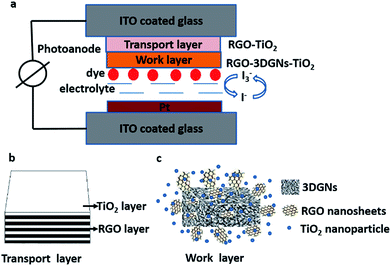 |
| | Scheme 1 Structures of (a) DSSCs, (b) transport layer and (c) work layer of the photoanode. | |
Results and discussion
SEM images of the pure TiO2, RGO–TiO2, 3DGNs–TiO2 and RGO–3DGNs–TiO2 composite photoanode are shown in Fig. 1a–d. The similar appearances of the 3DGNs–TiO2 and RGO–3DGNs–TiO2 indicates that the uniform distribution of TiO2 nanoparticles maintains after adding the RGO nanosheets, which is in line with our previous reports.11,16 In order to give full play to the function of the 3DGNs, its thickness and mass fraction have been optimized, and a bi-layer construction of the 3DGNs and 1 wt% percentage is found as the proper parameters.11,16,18 TEM images of the pristine 3DGNs and the prepared RGO–3DGNs–TiO2 are displayed in Fig. 2. The bi-layer structure of the 3DGNs can be proven by its cross-section image (inset of Fig. 2a), and the TiO2 nanoparticles can be identified by the lattice spacing (0.35 nm is ascribed to (101) plane of TiO2, HRTEM image in Fig. 2b). Raman curves can be used to judge the quality and average size of graphene samples. There are three major signal peaks, which named G, D and 2D band, can be seen in the Raman curves of the adopted RGO nanosheets and 3DGNs (Fig. S1 in the ESI†).23–25 The G band origins from the breath vibration of honeycomb carbon atoms associated with the E2g phonon at the Brillouin zone center. The D peak is caused by the discontinuous structure and defects of graphene samples, while the 2D peak is the second order of the D peak (resulting from the double resonant Raman scattering with two-phonon emissions) but free of defects. The small ID/IG value of the prepared RGO nanosheets demonstrates its low defect density, and no obvious change of this ratio can be seen for the RGO–TiO2 sample, implying that the influence on the graphene quality from following hydrothermal reaction can be ignored. According to the ratio of ID/IG, the average size of the adopted RGO nanosheets is ∼80 nm.9,16,22 It is worth noting that a visible D peak appears in the corresponding pattern of the 3DGNs, which is well-designed to endow an enhanced contact between the graphene basal plane and TiO2 (promoting the transport of the photo-induced electrons from TiO2 to graphene). Based on our previous work, the 3DGNs with a moderate defect density (1.35 × 109 cm−2) is recommended (detailed calculation about the defect density according to the Raman curve is supplied in ESI†).18
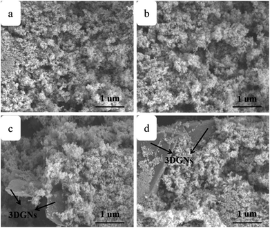 |
| | Fig. 1 SEM images of (a) TiO2, (b) RGO nanosheets–TiO2, (c) 3DGNs–TiO2 and (d) RGO nanosheets–3DGNs–TiO2. | |
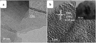 |
| | Fig. 2 TEM images of the (a) 3DGNs, the inset of HRTEM image displays its bi-layer structure (b) the RGO nanosheets–3DGNs–TiO2 composite, TiO2 nanoparticles can be identified by lattice spacing from the high magnification image. The low magnification image is shown in the inset. | |
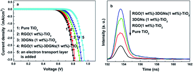
J–V curves of these resulting devices by using various photoanodes are shown in Fig. 3a. Compared with that case of using a pure TiO2 photoanode, photovoltaic performances including the short-circuit current density (JSC), open-circuit voltage (VOC) and fill factor (FF) significantly increase, and the RGO nanosheets and 3DGNs co-modified sample shows the best properties. A higher JSC means that more photo-generated electrons can reach electron collector through the dye molecules, TiO2, graphene basal plane and conductive glass (the detailed electron transport between them is provided in the Fig. S2 of ESI†). Several factors determine the resulting JSC, including the total amount of the photo-induced electrons and the loss amount during the transport process. There are two types of loss can be classified: the loss in the inner of each material (graphene, TiO2 and dye) and the loss at their interface. Firstly, the total amount of photo-induced electrons is decided by the adsorbed amount of dye molecules on the photoanode surface and the incident photon-to-current conversion efficiency (IPCE). Based on the similar BET areas, dye adsorption amounts (Table 1) and IPCE curves (Fig. 3b) of various devices, the difference between total amounts of the photo-induced electrons from various photoanodes is inconspicuous, which is proven by the photo current results (inset of Fig. 3b). Therefore, the determinant for the further improved photovoltaic performance of the RGO–3DGNs–TiO2 modified photoanode compared with that of the 3DGNs–TiO2 assisted samples is the electron transport process rather than the yield of the photo-generated electrons.
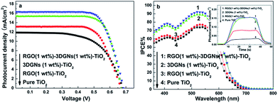 |
| | Fig. 3 (a) J–V curves and (b) IPCE curves of the resulting DSSCs with different photoanodes, the inset shows photocurrent of various photoanodes. | |
Table 1 Photovoltaic properties and dye loading of the resulting DSSCs with varied photoanodes. All measurements were recorded under AM-1.5G one sun and the active areas were ca. 0.15 cm2 for all cells
| Photoanode |
JSC (mA cm−2) |
VOC (mV) |
FF (%) |
η (%) |
Adsorbed dye (×10−7 mol cm−2) |
BET area (m2 g−1) |
| Pure TiO2 |
11.9 |
683 |
61.0 |
4.96 |
0.87 |
49.8 |
| RGO–TiO2 |
13.9 |
669 |
63.1 |
5.86 |
0.94 |
66.5 |
| 3DGNs–TiO2 |
15.4 |
673 |
63.5 |
6.58 |
1.05 |
117.7 |
| RGO–3DGNs–TiO2 |
16.3 |
682 |
63.7 |
7.08 |
1.07 |
129.5 |
As we known, the loss of electrons during their transport progress is induced by the introduced defects and boundaries. Moreover, the collision between the electron–electron and electron–phonon also shorten the lifetime of the photo-generated electrons (which determine the mean free path of electrons in a perfect sample). Considering the identical TiO2 raw material, the discrepancies of the transport ability from the adopted graphene and interface areas lead to the observed distinctions of photovoltaic performances. In fact, the 3DGNs have been proven a better candidate to modify TiO2 for a photoanode because of its natural 3D structure (providing an electron transport network for photo-induced electrons) and high quality (reducing the loss of electrons from the electron-defect collision).16,26,27 Based on this view of point, the additional RGO nanosheets in the 3DGNs–TiO2 photoanode should degrade the resulting performance due to the added resistance (and defect), which contradict with the experiment findings. There are two probably reasons can bring about the positive effect from the RGO nanosheets: an improved electron transport capacity at the interface and an enhanced synergy between the 3DGNs and TiO2. The EIS curves of the various samples are shown in Fig. 4, and two semicircles can be seen in the high-frequency and middle-frequency regions of all the profiles. Similar intensities of the semicircles in the high-frequency areas reflect that the impedance of the charge transfer in the counter electrode is almost uniform because of the identical Pt electrode.28 On the other hand, the significant differences can be observed from the signal in the middle-frequency area, indicating the prominent distinction of the charge transport processes at the photoanode–electrolyte interface from various devices.7 The additional RGO nanosheets (1 wt%) promote the electron transport, resulting from the presence of the surface functional groups which act as a bridge to link the graphene basal plane and TiO2 nanoparticles.21,22 The photo-induced electron utilization ratio is determined by the resistance of the whole photoanode, including resistance components from the TiO2, 3DGNs, RGO nanosheets and their interface areas. After adding a certain amount of the RGO nanosheets, the total resistance should be increased. However, the increased FF means the improved electron utilization ratio of the device by using the RGO nanosheets–3DGNs–TiO2 photoanode (Table 1), implying the negative effect from the RGO modifier can be offset by the reduced interface resistance, resulting from the surface functional groups of the RGO nanosheets.
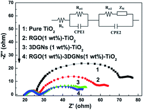 |
| | Fig. 4 EIS curves of the resulting devices with various photoanodes. | |
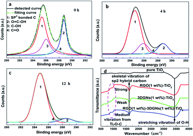
In order to further confirm the conclusion, RGO nanosheets with various reduction degrees are adopted to modify the 3DGNs–TiO2 photoanode. The specific reduction degree can be abstracted by their XPS curves, and the characteristic signals C1s of elemental carbon atoms and carbon atoms from the HO–C![[double bond, length as m-dash]](https://www.rsc.org/images/entities/char_e001.gif) O are located at 284.7 and 288.7 eV, respectively. After an elaborate fitting, the contributions from the CO and C–OH at 287.4 eV and 285.9 eV can be found (Fig. 5a–c).29 With a prolonged reduction time, the corresponding integral intensity of the C1s from functional groups decreases obviously, indicating the improved reduction degree of the RGO nanosheets. According to the evolution of the XPS curves, the ratio of the elemental carbon atoms increases from 42% (without a reduction procedure) to 93% (the reduction time is 12 h). By using these RGO samples to modify photoanodes, remarkable changes from the resulting photovoltaic performances can be obtained (Table 2), demonstrating the determined influence from the surface functional group amount of the adopted RGO nanosheets. In the case of adopting the sample with a low amount of functional group, the resulting JSC is inferior to that case of using the 3DGNs–TiO2, confirming an optimizing progress is the pre-condition to achieve the positive effect from the additional RGO nanosheets. After optimizing, a 4 h reduction time and 1 wt% mass fraction of the RGO nanosheets are recommended (Table 2). It is easy to understand a moderate amount of functional groups is beneficial to the resulting high performances. Excess residual functional groups cannot continuously improve electron transport ability because the total amount of photo-induced electrons keeps a constant when the adsorbed amount of dye molecules is fixed. Moreover, the high defect density of the RGO nanosheets brings about an additional resistance as well as a reduced FF, which is proven by the experimental results (Table 2). On the other hand, insufficient functional groups and a low mass fraction of the RGO nanosheets could not provide enough transport channels for electrons.
O are located at 284.7 and 288.7 eV, respectively. After an elaborate fitting, the contributions from the CO and C–OH at 287.4 eV and 285.9 eV can be found (Fig. 5a–c).29 With a prolonged reduction time, the corresponding integral intensity of the C1s from functional groups decreases obviously, indicating the improved reduction degree of the RGO nanosheets. According to the evolution of the XPS curves, the ratio of the elemental carbon atoms increases from 42% (without a reduction procedure) to 93% (the reduction time is 12 h). By using these RGO samples to modify photoanodes, remarkable changes from the resulting photovoltaic performances can be obtained (Table 2), demonstrating the determined influence from the surface functional group amount of the adopted RGO nanosheets. In the case of adopting the sample with a low amount of functional group, the resulting JSC is inferior to that case of using the 3DGNs–TiO2, confirming an optimizing progress is the pre-condition to achieve the positive effect from the additional RGO nanosheets. After optimizing, a 4 h reduction time and 1 wt% mass fraction of the RGO nanosheets are recommended (Table 2). It is easy to understand a moderate amount of functional groups is beneficial to the resulting high performances. Excess residual functional groups cannot continuously improve electron transport ability because the total amount of photo-induced electrons keeps a constant when the adsorbed amount of dye molecules is fixed. Moreover, the high defect density of the RGO nanosheets brings about an additional resistance as well as a reduced FF, which is proven by the experimental results (Table 2). On the other hand, insufficient functional groups and a low mass fraction of the RGO nanosheets could not provide enough transport channels for electrons.
 |
| | Fig. 5 XPS patterns of the adopted RGO nanosheets with various reduction times (a–c) 0 h, 4 h and 12 h, (d) IR profiles of the various photoanodes. | |
Table 2 Relationship between photovoltaic properties of the resulting DSSCs with varied mass fractions and reduction degrees of RGO nanosheets in the RGO nanosheets–3DGNs–TiO2 photoanodes. All measurements were recorded under AM-1.5G one sun and the active areas were ca. 0.15 cm2 for all cells
| Content and reduction time of the adopted RGO |
JSC (mA cm−2) |
VOC (mV) |
FF (%) |
η (%) |
Adsorbed dye (×10−7 mol cm−2) |
BET area (m2 g−1) |
| 0.5% and 0 h |
14.7 |
680 |
63.8 |
6.38 |
0.92 |
84.8 |
| 0.5% and 4 h |
14.8 |
672 |
63.6 |
6.33 |
0.91 |
73.0 |
| 1% and 0 h |
15.2 |
677 |
63.0 |
6.48 |
0.96 |
118.3 |
| 1% and 4 h |
16.3 |
682 |
63.7 |
7.08 |
1.07 |
129.5 |
| 1% and 12 h |
14.8 |
679 |
63.3 |
6.36 |
1.07 |
127.2 |
| 2% and 4 h |
15.8 |
668 |
63.2 |
6.67 |
1.09 |
173.1 |
| 2% and 12 h |
14.1 |
671 |
63.1 |
5.97 |
1.01 |
170.9 |
| 3% and 0 h |
15.3 |
671 |
62.8 |
6.45 |
1.12 |
184.3 |
| 3% and 4 h |
15.7 |
673 |
62.6 |
6.61 |
1.10 |
179.4 |
The dark currents of various photoanodes are shown in the Fig. 6a, the corresponding value from the RGO–3DGNs–TiO2 photoanode is smaller than that of the 3DGNs–TiO2 photoanode when the voltage exceeds 0.6 V, indicating that the improved contact between the conductive glass and photoanode is because of the presence of functional groups of the RGO nanosheets. Moreover, the tested lifetime of the photo-generated electrons also confirms this point of view (Fig. 6b). About an 8% extension for the electron lifetime can be obtained after adding the RGO nanosheets, resulting from the depressed recombination of the photo-induced electrons and I3− ions at the interface of the conductive substrate and photoanode. Further, IR curves are recorded to reveal the contact between the graphene basal plane and TiO2 nanoparticles in various photoanodes (Fig. 5d). The low frequency absorption signal below 1000 cm−1 is assigned to the Ti–O–Ti vibration,30 while the broad absorption peak ranged from 3000 to 3700 cm−1 is introduced by the O–H stretching vibration of the surface hydroxyl from adsorbed water.31 After adding the graphene modifier, an absorption peak around 1600 cm−1 which is attributed to the skeletal vibration of the graphene sheets can be seen.32 By comparing the IR profiles of the pure graphene sample and the composite photoanodes, a new signal located at 790 cm−1 can be seen, which is suggested as a combination of the Ti–O–Ti and Ti–O–C vibrations,33–35 indicating the formation of a chemical bond between the graphene basal plane and TiO2 particles. According to the previous reports, the chemical bond between the RGO nanosheets and TiO2 can be built through the residual surface hydroxyl groups of the graphene basal plane.33,35 Therefore, the additional RGO nanosheets with a controllable functional group amount will enhance the bonding behaviour, which is consistent with IR profiles of the RGO–3DGNs–TiO2 and 3DGNs–TiO2 photoanodes (the corresponding signal intensity increases after adding the RGO nanosheets). Therefore, both the contacts between the conductive substrate and photoanode and between the graphene basal plane and TiO2 particles are enhanced after adding the RGO nanosheets.
 |
| | Fig. 6 (a) Dark currents of devices with various photoanodes and (b) lifetimes of the photo-induced electrons in various photoanodes. | |
Besides facilitating the electron transport, the possible influence from the additional RGO nanosheets on light scattering in the photoanode is also studied (the light scattering ability imposes a significant influence on the photon absorbing amount of dye molecules). The UV-visible diffuse scattering spectra of various photoanodes are shown in Fig. 7. Without loading the dye molecules, the light-harvesting efficiency of the photoanode enhances prominently after adding the RGO nanosheets, resulting from the similar size of the RGO nanosheets cluster (these nanosheets tend to agglomerate together due to electrostatic interaction) and wavelength of the incident-light (Fig. 7a). After loading the dyes, although the scattering intensities of all the photoanodes decrease due to the high absorption ability of the dye molecules, the corresponding intensity of the RGO–3DGNs–TiO2 photoanode is still stronger than that of the 3DGNs–TiO2 photoanode (Fig. 7b). Therefore, the presence of the RGO nanosheets not only provides a better linker for the electron transport between the graphene basal plane and TiO2 nanoparticles, but also brings about a better photon scattering ability for the resulting photoanode. Both the functions promote the photovoltaic performances of the resulting DSSCs.
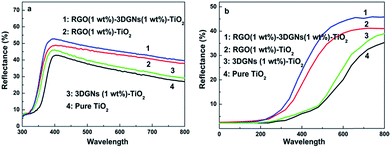 |
| | Fig. 7 UV-visible diffuse reflectance spectra of various photoanodes (a) without dye loading; (b) with dye loading. | |
In our previous work, an additional transport layer between the photoanode (work layer) and conductive glass is recommended, which decreases the dark current by depressing the recombination of the photo-induced electrons and I3− ions.9 The transport layer is composed of the alternative RGO nanosheets and TiO2 nanosheets to achieve a close contact between the work layer and conductive substrate. Naturally, whether a similar influence from the surface functional groups of the adopted RGO nanosheets on the performance of the transport layer deserves to reveal. The composite photoanodes including a work layer and a transport layer are fabricated (more details are provided in the ESI†).9,11 Therein, the RGO nanosheets with various reduction degrees are adopted to prepare the transport layer, and the corresponding performances are listed in the Table 3. The resulting photovoltaic performances manifest that the additional transport layer brings about a superior performance to the devices (Fig. 8). However, no prominent influence from the reduction degree of the adopted RGO nanosheets can be found, indicating the function of the transport layer is independent on the functional groups of the RGO nanosheets, which is different from that case of the work layer. In order to understand this phenomenon, the transport mechanism of the work layer and the transport layer should be discussed. As for the work layer, our group found that the electron transport between the graphene and TiO2 is based on the quantum tunnel effect.35 Therefore, the height and width of the Schottky barrier between the graphene basal plane and TiO2 determine the resulting electron transport ability, which is closely related to the interface condition between them. The surface functional groups of the additional RGO nanosheets improve the interface contact by providing a bridge to link the graphene basal plane and TiO2 particles. Therefore, the presence of the RGO nanosheets with an optimized reduction degree imposes a significantly positive influence on the resulting performance of the DSSCs (Table 2). On the other hand, the electron transfer during the transport layer relies on the continuous RGO structure (diffusion mechanism rather than quantum tunneling), and the influence from interface can be ignored.9,35 In the transport layer, the RGO nanosheets in the alternant bi-layers (RGO nanosheets layer and TiO2 nanosheets layer) can contact to each other because of the nano-scaled TiO2 nanosheets.9 The electron transport during the transport layer has nothing to do with the interface between the RGO nanosheets and TiO2 nanosheets. Therefore, the performance of transport layer is determined by its thickness (the continuity of the RGO nanosheets in the normal direction) rather than the reduction degree of the RGO nanosheets (Table 3).
Table 3 Photovoltaic properties of the resulting DSSCs with varied reduction degrees of RGO nanosheets in the transport layer. All measurements were recorded under AM-1.5G one sun and the active areas were ca. 0.15 cm2 for all cells
| Number of the RGO–TiO2 bi-layers |
Reduction time of the RGO |
JSC (mA cm−2) |
VOC (mV) |
FF (%) |
η (%) |
| 50 |
0 h |
16.1 |
675 |
63.9 |
6.94 |
| 4 h |
16.3 |
671 |
64.0 |
6.99 |
| 12 h |
16.4 |
672 |
63.8 |
7.03 |
| 100 |
0 h |
16.9 |
677 |
64.2 |
7.24 |
| 4 h |
16.5 |
669 |
64.5 |
7.12 |
| 12 h |
16.4 |
663 |
64.5 |
7.01 |
| 200 |
0 h |
17.1 |
671 |
64.1 |
7.35 |
| 4 h |
17.5 |
679 |
64.6 |
7.68 |
| 12 h |
17.4 |
676 |
64.7 |
7.61 |
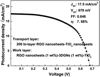 |
| | Fig. 8 J–V curve of a preliminarily optimized device based on the photoanode with a transport layer and a work layer under AM-1.5G one sun intensity. | |
Based on the above analysis, an optimized composite photoanode with a work layer and a transport layer is fabricated by the RGO nanosheets, 3DGNs (1 wt%) and TiO2. Therein, an additional 1 wt% RGO nanosheets (the reduction time is 4 h) is adopted for the work layer, while a 200 bi-layer RGO–TiO2 alternative structure is utilized as the transport layer. After optimizing, the JSC and VOC reach 17.5 mA cm−2 and 679 mV, respectively, manifesting the remarkably enhanced photo-induced electron utilization ratio. The FF increases to 0.646, resulting from the reduced resistance of the interface fields (between the graphene basal plane and TiO2 particles, and between the photoanode and conductive substrate). A η as high as 7.68% can be achieved, which is 31% and 16% higher than those cases of the previous reported RGO–TiO2 and 3DGNs–TiO2 based devices.9,11,36 In fact, the η can be further improved by optimizing the combination of the 3DGNs and RGO nanosheets, which is under study.
Experimental
Materials
Natural graphite was obtained from Alfa Aesar Co. TiO2 nanoparticles were purchased from Degussa. Acetonitrile, polytetrafluoroethylene and sodium dodecyl sulfate (SDS) were obtained commercially from the Beijing chemical reagent plant (Beijing, China). Polyethyleneimine (PEI) aqueous solution, chloroplatinic acid, indoline, iodine and potassium iodide were purchased from Aladdin Co. Deionized water (resistivity 18 MΩ cm) was utilized to prepare all aqueous solutions. The TiO2 nanoparticles were sintered at 400 °C for 2 h to remove the organics and dust for the subsequent experiments.
Preparation
The preparation of the RGO nanosheets, 3DGNs, pure TiO2 photoanode, RGO–TiO2 photoanode, 3DGNs–TiO2 photoanode, Pt electrode, RGO–TiO2 nanosheets transport layer and DSSCs have been reported by our previous reports.9,11,16 Briefly, the RGO–3DGNs–TiO2 photoanode is prepared as following: the 3DGNs (1 wt%) and RGO nanosheets (0.5 wt%, 1 wt%, 2 wt% and 5 wt%) were mixed with TiO2 nanoparticles and moved into an ethanol solution for the supersonic treatment (20 min). Afterward, the resulting paste was deposited on the conductive glass (or transport layer) by the doctor-blade approach.
Characterization
X-ray photoelectron spectroscopy (XPS) was measured on an RBD upgraded PHI-5000C ESCA system (Perkin Elmer). The morphology images were obtained by the scanning electron microscope (SEM) (FEI Sirion 200 scanning electron microscope) and the transmission electron microscopy (TEM) (JEM-2100F). Raman spectra were recorded by a LabRam-1B Raman micro-spectrometer at 514.5 nm (Horiba Jobin Yvon, France). The BET surface areas were measured on a Nova 100 by using N2 as the adsorption gas. Infrared spectroscopy (IR) curves were measured on an IR Prestige-21 system (PerkinElmer). UV-visible diffuse reflectance spectra were carried out on a TU-1901 UV-visible spectrophotometer. Photocurrent measurements and electrochemical impedance spectroscopy (EIS) were performed on a CHI 660D electrochemical analyser (Shanghai CH Instrument Company, China). The J–V curves were recorded by a PGSTAT 30 potentiostat (Netherlands). The incident photon-to-current conversion efficiency (IPCE) profiles were recorded on a Newport 1918-c power meter.
Conclusions
A series of photoanodes based on the RGO nanosheets, 3DGNs and TiO2 nanoparticles have been prepared. The presence of the well-designed RGO nanosheets exerts a positive influence to enhance the resulting performances of the DSSCs because of the connecting function of their surface functional groups to improve the electron transport at the interface fields. The reduction degree and mass fraction of the adopted RGO nanosheets are closely related to the resulting photovoltaic properties. In fact, the 3DGNs provide a fast transport network for the photo-induced electrons, and the RGO nanosheets further improve the electron transport at the interface between the graphene basal plane and TiO2. Moreover, an additional transport layer further enhances the JSC and FF of the resulting DSSCs. After optimizing the structure of the resulting photoanode, a η as high as 7.68% was achieved, indicating a promising prospect of the RGO nanosheets and 3DGNs co-modified DSSCs.
Conflicts of interest
There are no conflicts to declare.
Acknowledgements
This work was supported by the National Natural Science Foundation of China (51506012, 51472035, 51572036); Natural Science Foundation of Jiangsu Province (BK20150266); Changzhou key laboratory of graphene-based materials for environment & safety (CM20153006, CE20160001-2).
Notes and references
- B. C. Nath, D. Das, I. R. Kamrupi, K. J. Mohan, G. A. Ahmed and S. K. Dolui, RSC Adv., 2015, 5, 95385–95393 RSC.
- D. W. Zhang, X. D. Li, H. B. Li, S. Chen, X. J. Yin and S. M. Huang, Carbon, 2011, 49, 5382–5388 CrossRef CAS.
- S. L. Li, H. H. Min, F. Xu, L. Tong, J. Chen, C. Y. Zhu and L. T. Sun, RSC Adv., 2016, 6, 34546–34552 RSC.
- H. J. Ahn, I. H. Kim, J. C. Yoon, S. I. Kim and J. H. Jang, Chem. Commun., 2014, 50, 2412–2415 RSC.
- P. S. Chandrasekhar and V. K. Komarala, RSC Adv., 2015, 5, 84423–84431 RSC.
- S. R. Sun, L. Gao and Y. Q. Liu, Appl. Phys. Lett., 2010, 96, 083113–083115 CrossRef.
- T. H. Tsai, S. C. Chiou and S. M. Chen, Int. J. Electrochem. Sci., 2011, 6, 3333–3343 CAS.
- L. C. Chen, C. H. Hsu, P. S. Chan, X. Y. Zhang and C. J. Huang, Nanoscale Res. Lett., 2014, 9, 380–386 CrossRef PubMed.
- B. Tang and G. X. Hu, J. Power Sources, 2012, 220, 95–102 CrossRef CAS.
- Z. P. Chen, C. W. Ren, L. B. Gao, B. L. Liu, S. F. Pei and H. M. Cheng, Nat. Mater., 2011, 10, 424–428 CrossRef CAS PubMed.
- Y. F. Sun, Y. C. Cao, W. Q. Huang, Y. J. Zhu, L. Heng and B. Tang, Mater. Lett., 2016, 165, 178–180 CrossRef CAS.
- H. D. Jang, E. H. Jo, H. Chang, J. Kim and K. M. Roh, Mater. Lett., 2015, 142, 304–307 CrossRef CAS.
- Y. Y. Zhu, X. Meng, H. J. Cui, S. P. Jia, J. H. Dong, J. F. Zheng, J. H. Zhao, Z. J. Wang, L. Li, L. Zhang and Z. P. Zhu, ACS Appl. Mater. Interfaces, 2014, 6, 13833–13840 CAS.
- M. Y. Yen, M. C. Hsiao, S. H. Liao, P. Liu, H. M. Tsai and C. M. Ma, Carbon, 2011, 49, 3597–3606 CrossRef CAS.
- J. Zhi, H. L. Cui, A. Chen, Y. Xie and F. Q. Huang, J. Power Sources, 2015, 281, 404–410 CrossRef CAS.
- B. Tang, G. X. Hu and Z. X. Shi, J. Power Sources, 2013, 234, 60–68 CrossRef CAS.
- Y. H. Zhang, N. Zhang, Z. R. Tang and Y. J. Xu, Phys. Chem. Chem. Phys., 2012, 14, 9167–9175 RSC.
- B. Tang, S. L. Wang, J. Zhang, Z. W. Wang, Y. F. He and W. Q. Huang, Int. Mater. Rev., 2017 DOI:10.1080/09506608.2017.1344377.
- B. Tang and G. X. Hu, J. Phys. Chem. C, 2013, 117, 25175–25184 CAS.
- B. Tang and G. X. Hu, Chem. Vap. Deposition, 2014, 20, 14–22 CrossRef CAS.
- Y. F. Sun, B. Tang, W. Q. Huang, S. L. Wang and Z. W. Wang, Appl. Therm. Eng., 2016, 103, 892–900 CrossRef CAS.
- B. Tang, G. X. Hu and H. Y. Gao, Int. J. Heat Mass Transfer, 2015, 85, 420–429 CrossRef CAS.
- B. Tang, G. X. Hu and H. Y. Gao, Appl. Spectrosc. Rev., 2010, 45, 369–407 CrossRef CAS.
- M. Kalbac, V. Vales and J. Vejpravova, RSC Adv., 2014, 4, 60929–60935 RSC.
- S. Mateti, M. M. Rahman, L. H. Li, Q. Cai and Y. Chen, RSC Adv., 2016, 6, 35287–35294 RSC.
- Y. F. Sun, X. B. Wang, B. Tang and J. M. Ban, Mater. Lett., 2017, 189, 54–57 CrossRef CAS.
- Y. Ma and Y. Chen, Natl. Sci. Rev., 2015, 2, 40–53 CrossRef.
- P. Dong, C. L. Pint, M. Hainey, F. Mirri, Y. Zhan, J. Zhang, M. Pasquali, R. H. Hauge, R. Verduzco, M. Jiang, H. Lin and J. Lou, ACS Appl. Mater. Interfaces, 2011, 3, 3157–3161 CAS.
- P. K. Sahoo, B. Panigrahy and D. Bahadur, RSC Adv., 2014, 4, 48563–48571 RSC.
- B. Neumann, P. Bogdanoff, H. Tributsch, S. Sakthivel and H. Kisch, J. Phys. Chem. B, 2005, 109, 16579–16586 CrossRef CAS PubMed.
- H. Zhang, X. J. Lv, Y. M. Li, Y. Wang and J. H. Li, ACS Nano, 2010, 4, 380–386 CrossRef CAS PubMed.
- Q. Xiao, J. Zhang, C. Xiao, Z. Si and X. Tan, Sol. Energy, 2008, 82, 706–713 CrossRef CAS.
- Q. Q. Zhai, B. Tang and G. X. Hu, J. Hazard. Mater., 2011, 198, 78–86 CrossRef CAS PubMed.
- J. Pouilleau, D. Devilliers and H. P. Groult, J. Mater. Sci., 1997, 32, 5645–5651 CrossRef CAS.
- G. X. Hu and B. Tan, Mater. Chem. Phys., 2013, 138, 608–614 CrossRef CAS.
- H. Choi, H. Kim, S. Hwang, Y. Han and M. Jeon, J. Mater. Chem., 2011, 21, 7548–7551 RSC.
Footnote |
| † Electronic supplementary information (ESI) available: Calculation of graphene size and defect density, electrical structure of dye molecules, TiO2, graphene and conductive substrate. See DOI: 10.1039/c7ra09135d |
|
| This journal is © The Royal Society of Chemistry 2017 |
Click here to see how this site uses Cookies. View our privacy policy here. 
 Open Access Article
 This Open Access Article is licensed under a
  *,
Guojian Ji,
Zhengwei Wang,
Haiqun Chen*,
Xufei Li,
Haogang Yu,
Sen Li and
Hong Liu
*,
Guojian Ji,
Zhengwei Wang,
Haiqun Chen*,
Xufei Li,
Haogang Yu,
Sen Li and
Hong Liu


