
 Open Access Article
 This Open Access Article is licensed under a
 Creative Commons Attribution 3.0 Unported Licence
Effect of BCP buffer layer on eliminating charge accumulation for high performance of inverted perovskite solar cells†
Chuanliang Chen ,
Shasha Zhang,
Shaohang Wu,
Wenjun Zhang,
Hongmei Zhu,
Zhenzhong Xiong,
Yanjun Zhang and
Wei Chen*
,
Shasha Zhang,
Shaohang Wu,
Wenjun Zhang,
Hongmei Zhu,
Zhenzhong Xiong,
Yanjun Zhang and
Wei Chen*
Wuhan National Laboratory for Optoelectronics, Huazhong University of Science and Technology, 1037 Luoyu Road, Wuhan 430074, China. E-mail: wnlochenwei@mail.hust.edu.cn
First published on 19th July 2017
Abstract
Bathocuproine (BCP) buffer layer has been commonly used in inverted p–i–n perovskite solar cells (PSCs) for high performance, but its working mechanism has not been thoroughly elucidated. Here, a series of devices have been fabricated with controlled thicknesses of BCP layers deposited by thermal evaporation. With the aid of J–V data fitting by a single-diode model, the effect of BCP layer thickness on the device performance has been identified. An optimal power conversion efficiency (PCE) up to 17.9% has been obtained for the device with a critical BCP thickness of 5 nm, thanks to the formation of ohmic contact and reduction of interfacial charge recombination. While if the BCP layer is too thin or too thick, charge accumulation will emerge due to different mechanisms and lead to device performance degradation, which have been clearly confirmed by capacitance–voltage (C–V) characteristic displaying a peak capacitance at a certain bias region under illumination. The insertion of such a critical thin BCP layer between PCBM and Ag also resulted in long-term stability improvement of the devices, of which the T80 lifetime increased from ∼6 hours to ∼50 hours in ambient air. This work gives insight into improving PSCs' performance through buffer layer's optimization, and the measurement of C–V characteristic provides a new clue to detect the defection of photovoltaic device associated with charge accumulation.
Introduction
Perovskite solar cells (PSC) have been intensively investigated since the organometal halide perovskites were used as sensitizers for photoelectrochemical cells in 2009,1 and its power conversion efficiency (PCE) has dramatically risen from 3.8% since then to currently 22.1%.2–6 The state of art PSCs have been reported with diverse device structures, such as regular mesoporous/planar structure with n–i–p layouts2,3,6 and inverted planar structure with p–i–n layouts.4,5 In the early stage of PSC research, the regular structure was more frequently reported. Later on, researchers gradually recognized the intrinsic drawbacks of some frequently used interfacial materials in the regular devices, such as compact TiO2 with charge extraction difficulty and spiro-OMeTAD with moisture sensitive (Li-, Co-salts)7 and perovskite destructive additive (TBP).8 Therefore, currently, increasing attention has been paid to the inverted planar structure, in order to explore different combinations of interfacial materials and their impacts on the photovoltaic behaviors.9–18The first inverted PSC employed the structure of indium titanium oxide (ITO)/poly(3,4-ethylenedioxythiophene):poly(styrene-sulfonate) (PEDOT:PSS)/CH3NH3PbI3/PCBM/bathocuproine (BCP)/Al, emerged in 2013 and obtained only a 3.9% efficiency.9 Afterwards, researchers step-by-step improved the efficiency of inverted PSCs over 10% by optimizing perovskite film's morphology, introducing high work function NiOx interfacial layer to replace PEDOT:PSS and better deposition methods of NiOx layer.7,19 Seok and coworkers got a 14.1% efficiency through optimizing PCBM thickness and inserting LiF as buffer layer.11 A more superior performance was gained by Chen et al. based on the device structure of fluorine-doped tin oxide (FTO)/NiMg(Li)O/CH3NH3PbI3/PCBM/Ti(Nb)Ox/Ag: the PCE was elevated to 18.3% for small area (0.09 cm2) device and 15.0% (certified data) for large area (1 cm2) device.5 Recently, the certified PCE of large area (1 cm2) inverted device has been risen to 18.2% by the same group though perovskite/PCBM heterojunction engineering.8 In those previous literatures, an extremely thin layer of BCP, LiF or Ti(Nb)Ox was commonly used as buffer layer in the devices, which was inserted between PCBM and metal cathode and had great influence to the device performance.20–22 However, the role and working mechanism of buffer layer have not been elucidated thoroughly in PSC system.
In this study, the devices with inverted planar structure of FTO/NiMg(Li)O (20 nm)/perovskite (450 nm)/PCBM (60 nm)/BCP (x nm)/Ag (80 nm) with controlled BCP thicknesses have been fabricated. The BCP layers were deposited by thermal evaporation which was suitable for fabricating large-area device and exactly controlling the film thickness. The optimized device with a 5 nm-thick BCP layer has achieved the champion PCE of 17.9% under simulated AM 1.5G 100 mW cm−2 solar light, while 0 nm-thick and 13 nm-thick BCP layers have resulted in PCEs of 14.1% and 2.6% respectively. This demonstrated how critical the BCP thickness could influence the device performance. To clarify the working mechanism of BCP layer, a single-diode model has been introduced to fit the thickness-dependent J–V curves. In addition, capacitance–voltage (C–V) measurement has been involved to help understanding.
Experimental details
Solar cell fabrications
The fluorine-doped tin oxide (FTO)-coated glass substrates were first ultrasonically cleaned with cleaning fluid, deionized water, alcohol, and acetone respectively for 20 minutes in sequence. The NiMg(Li)O-based hole extraction layer was then deposited onto FTO-glass by spray pyrolysis at 500 °C. The precursor solution was composed of nickel(II) acetylacetonate in a super-dehydrated acetonitrile and ethanol mixture.5 The CH3NH3PbI3 perovskite layer, with a thickness of about 450 nm, was deposited employing a reported method;3 this was followed by the deposition of a thin PCBM layer (60 nm) by spin-coating its chlorobenzol solution (20 mg mL−1) at 1500 rpm for 30 seconds. Subsequently, a BCP layer, used as buffer layer, was thermally evaporated under a high vacuum (<3 × 10⁻⁴ Pa). Finally, the device was completed by thermal evaporation of an 80 nm-thick Ag cathode. The device architecture is shown in Fig. 1(a) and its high-resolution cross-sectional SEM image is given in Fig. 1(b). | ||
| Fig. 1 (a) The device structure of FTO/NiMg(Li)O/CH3NH3PbI3/PCBM/BCP/Ag. (b) A high-resolution cross-sectional scanning electron microscopy (SEM) image of photovoltaic device with 5 nm-BCP buffer layer. | ||
Characterization
Cross-sectional image was taken on a high-resolution scanning electron microscope (Hitachi-4800) at a 10 kV accelerating voltage. A solar simulator (Oriel) fitted with a filtered 450 W xenon lamp was used to provide solar simulated irradiation. The photocurrent density–voltage (J–V) curves were measured using a Keithley 2400 source meter with scan rate of 0.1 V s−1 and the bias potential is in the range of −0.2 to 1.2 V. The light intensity of the simulated sunlight was calibrated to be 100 mW cm−2 by a standard c-Si solar cell and the effective area of the solar cell was defined to be 0.09 cm2 using a non-reflective metal mask. The capacitance–voltage (C–V) characteristics were measured on an electrochemical workstation (Zahner Zennium) under dark or illumination (LED white light, 60 mW cm−2). The frequency was set at 1 kHz and the bias potentials ranged from −0.2 to 1.2 V.Result and discussion
A series of devices with varying BCP layer thicknesses, based on the structure as depicted in Fig. 1(a), have been fabricated. Their forward scan J–V curves from high efficient and reproducible devices (typical devices) under simulated solar light (AM 1.5G, 100 mW cm−2) are shown in Fig. 2(a) and the performance parameters derived from the J–V curves are summarized in Table 1. For accurately exploring the impact of varying BCP thickness on photovoltaic performance, the parameters of every 10 samples with the same BCP thickness, including VOC, JSC, FF, and PCE, are listed in Table S1.† It is to be noted that the PCE increases firstly and then decreases with the increase of BCP thickness and achieves its highest value of 17.87% when the BCP thickness equals to 5 nm, the J–V curve of which is shown in Fig. 2(b). A similar trend is observed for JSC and FF (see Fig. 2(d) and (e)). It is obvious that the thickness of BCP buffer layer can significantly affect the parameters of JSC and FF, and then lead to the variation of PCE. The increase of JSC and FF might be attributed to smaller series resistances and lower recombination rates as the BCP thickness increases from 0 to 5 nm; while the decrease of JSC and FF as the BCP thickness further increases to 13 nm should be due to larger series resistances and higher recombination rates induced by too thick BCP layers. Just as shown in Fig. 2(a), S-shaped J–V curves emerge both at the BCP thickness of 0 nm and 13 nm, which imply two different barriers for the photo-induced electrons to tunnel through.23 It is worth pointing out that VOC keeps nearly identical when the BCP thickness varies from 0 to 5 nm (see Fig. 2(c)), which is mainly attributed to the fact that VOC depends mainly on the relative energy levels between LUMO level of PCBM and Evb of NiMgLiO; while if BCP thickness increases from 5 nm to 13 nm, the VOC would decrease gradually due to serious electron–hole recombination induced by charge accumulation emerging at the interface between BCP and PCBM. After optimizing the interface layers, the champion device with 5 nm thickness of BCP layer is obtained with VOC = 1.06 V, JSC = 21.2 mA cm−2, FF = 0.79, and PCE = 17.87%, the hysteresis phenomenon in this optimal device is negligible, as shown in Fig. 2(b).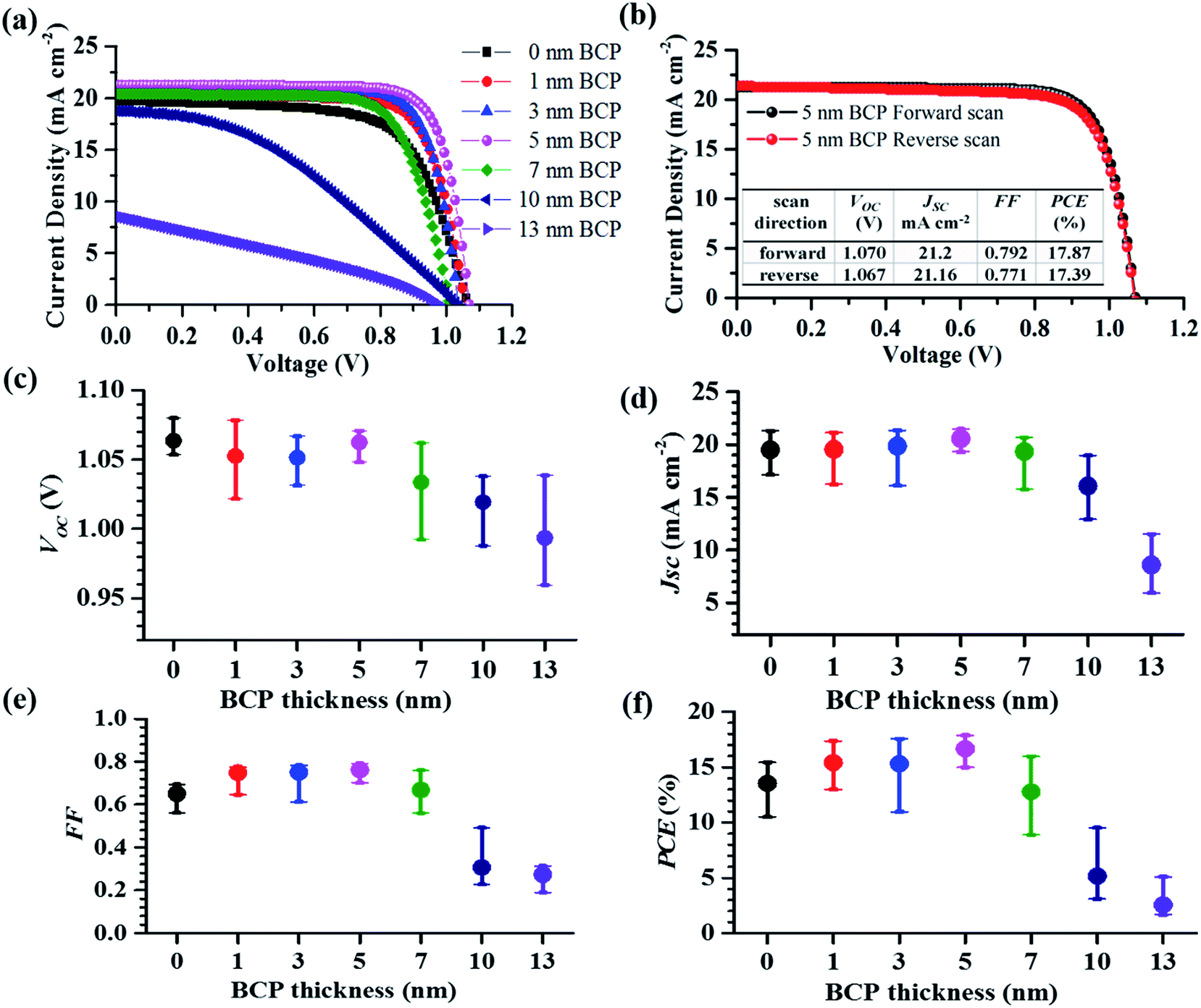 | ||
| Fig. 2 (a) The forward scan J–V curves of PSCs with varying BCP layer thicknesses, measured under simulated solar light (AM 1.5G, 100 mW cm−2). (b) J–V curves of the champion device with a BCP layer thickness of 5 nm. Dependences of (c) open-circuit voltage (VOC), (d) short-circuit photocurrent density (JSC), (e) fill factor (FF), (f) PCE on the corresponding thickness of BCP layer, 10 samples being included. | ||
| BCP thickness (nm) | VOC (V) | JSC (mA cm−2) | FF | PCE (%) |
|---|---|---|---|---|
| 0 | 1.071 | 19.67 | 0.66 | 14.07 |
| 1 | 1.055 | 20.38 | 0.75 | 16.18 |
| 3 | 1.036 | 20.94 | 0.78 | 16.83 |
| 5 | 1.070 | 21.11 | 0.79 | 17.87 |
| 7 | 1.039 | 19.70 | 0.73 | 14.92 |
| 10 | 1.032 | 18.64 | 0.39 | 7.44 |
| 13 | 0.976 | 8.66 | 0.31 | 2.64 |
To evaluate the effect of BCP buffer layer more clearly, a single-diode model24–26 has been employed to fit the series of J–V curves of the devices. The corresponding equivalent circuit is shown in Fig. 3(a). The J–V characteristic can be accordingly described by the following equation:
 | (1) |
 | (2) |
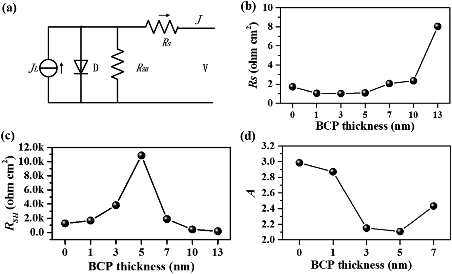 | ||
| Fig. 3 (a) The single-diode equivalent circuit model of the studied PSC, the dependences of the fitted parameters including (b) RS, (c) RSH, (d) A on the BCP layer thickness. | ||
It is clear that −dV/dJ and (JSC − J)−1 obeys a linear relationship. The plot of −dV/dJ vs. (JSC − J)−1 can yield the slope AVT and the intercept RS directly.27 Meanwhile, RSH can be deduced from the slope of J–V curve near zero bias under illumination. The fitted parameters based on the J–V curves in Fig. 2(a) are obtained by the above methods and summarized in Table 2. It is to be noticed that as the thickness of BCP layer increases from 0 to 13 nm, the series resistance RS decreases firstly and then increases significantly, which is shown in Fig. 3(b). An opposite trend is observed for RSH, as illustrated in Fig. 3(c). The fitted results are well consistent with the above speculation on BCP layers' roles on charge transfer and recombination.
| BCP thickness (nm) | RS (ohm cm2) | RSH (ohm cm2) | A |
|---|---|---|---|
| 0 | 1.72 | 1262 | 2.985 |
| 1 | 1.04 | 1665 | 2.87 |
| 3 | 1.02 | 3830 | 2.151 |
| 5 | 1.08 | 10![[thin space (1/6-em)]](https://www.rsc.org/images/entities/char_2009.gif) 862 862 |
2.108 |
| 7 | 2.06 | 1866 | 2.433 |
| 10 | 2.35 | 417 | 23.875 |
| 13 | 8.04 | 161 | 52.672 |
It is suggested that the changes of RS and RSH can be explained as follows. For the device with 0 nm-BCP layer, Schottky contact can be formed between PCBM and Ag cathode28 which would bring charge accumulation and relatively large series resistance, and then lead to degradation of device performance. However, such Schottky barrier height decided by the difference between the LUMO level of PCBM (−3.9 to 4.2 eV, different reports gave different values)5,9,11 and the work function of Ag (−4.3 eV versus vacuum) can only be 0.1–0.4 eV. Such charge transfer barrier is not very high, and just results in a small decrease on JSC (19.67 mA cm−2) compared to its optimal value (21.11 mA cm−2). Recombination will be increased to some extent, therefore, one may found RSH of 0 nm-BCP device (1262 ohm cm2) is smaller than the optimal device (10862 ohm cm2) at BCP thickness of 5 nm.
When a thin BCP layer is inserted between PCBM and Ag cathode, RS become smaller thanks to the formation of better ohmic contact and RSH becomes larger due to decrease of interfacial recombination. These are consistent with the device getting improvement of JSC and FF. Especially, when the BCP thickness equals to 5 nm, the parameters of RS = 1.08 ohm cm2, RSH = 10862 ohm cm2, both reach the optimal value, and the optimal device performance is achieved accordingly. However, when the BCP thickness is over 7 nm, RS becomes larger due to the low conductivity of BCP and RSH becomes smaller because more electron–hole recombination emerges due to the charge accumulation at the interface between PCBM and BCP layer. All of these result in serious degradation of device performance, as seen in Table 1. Another parameter, ideality factor (A), can be used to evaluate the process of carrier transport and carrier recombination in a PN junction solar cell.25 Here, A (see Fig. 3(d)) decreases from 2.87 to 2.11 when the BCP thickness varies form 0 nm to 5 nm, which means electron–hole recombination reduces due to better ohmic contact. Subsequently, with BCP thickness' continuous increasing from 5 nm to 13 nm, A increases from 2.11 to 52.67 attributed to charge accumulation which leads to serious recombination. And high efficiency can be obtained for the device with 5 nm-BCP layer accompanying a minimum A (2.11) which denotes carrier recombination decreases to the minimum. Therefore, the variation of circuit parameters could be attributed to charge accumulation at the “PCBM/Ag” Schottky type contact or “PCBM/thick-BCP” interface. Note that, these involve two different mechanisms of charge accumulation, one is induced by band alignment mismatch, and the other is induced by low conductivity of interfacial layer.21
The impact of BCP layer thickness on interfacial charge transport and recombination could be illustrated as Fig. 4. The two different charge accumulation mechanisms have been highlighted. For the device with 0 nm-BCP layer, small charge accumulation would emerge at the interface between PCBM and Ag cathode due to the existence of Schottky barrier (though not high), resulting in a little inferior device performance, which is shown in Fig. 4(a). When the thickness of BCP layer equals to the optimal value of 5 nm, the BCP layer is thick enough to fully cover the PCBM surface, eliminating the direct contact between PCBM/Ag. And meanwhile, 5 nm is thin enough for photo-induced electrons to tunnel across fluently. Therefore, in this condition, almost no charge accumulation emerges at the PCBM/BCP/Ag interfaces, which implies good ohmic contact has been established in-between these layers. Accordingly, the optimal device performance is achieved at this BCP layer thickness, which can be seen in Fig. 4(b). However, when the BCP thickness further increases to 13 nm, serious charge accumulation would emerge at the interface between PCBM and BCP layer owing to tunneling paths become too long. The device performance degrades dramatically because of electron–hole recombination, which is shown in Fig. 4(c).
 | ||
| Fig. 4 The energy diagram and charge transport mechanism of photovoltaic devices with varied BCP thicknesses, (a) device with 0 nm-BCP layer, (b) device with 5 nm-BCP layer, (c) device with 13 nm-BCP layer. | ||
To further confirm the charge accumulation described in Fig. 4, C–V characteristics of the devices with 0 nm, 5 nm and 13 nm BCP layers have been measured under dark and illumination. The quantity of electric charge (Q) can be calculated with follow equation of Q = CV. The peak in the C–V curve means the quantity of electric charge firstly increases and then decreases corresponding to a process of charge–discharge, indicating charge accumulation in the device. For the device with 5 nm-BCP layer, no peak capacitance could be found under illumination at bias below VOC, as shown in Fig. 5(b), which means there is no evident charge accumulation in the device. For the device with 0 nm-BCP layer, both under dark and illumination, a peak capacitance is clearly observed in the bias range between 0.9–1.1 V, as denoted in Fig. 5(a). Noting that just in the same bias range, the J–V curve of 0 nm-BCP based device became evidently inferior to the J–V curve of the optimal 5 nm-BCP based device. This phenomenon is consistent with the previous literature5 with the same PCBM/Ag Schottky contact. For the device with 13 nm-BCP layer, its C–V characteristic under dark has a gentle capacitance peak at the range of 0.4–0.8 V bias voltage because very few electron–hole pairs has been generated; however, under illumination condition, its capacitance (up to 103 nF) increases to several times higher than the 5 nm-BCP reference in the wide bias range of 0–0.8 V (Fig. 5(c)) and a peak capacitance appears at about 0.6 V bias rather than in the range of 0.9–1.1 V bias. This difference implies though the 13 nm BCP-based device also has charge accumulation, but its mechanism is different from the 0 nm-BCP based device. In the wide bias range of 0–0.8 V under illumination, serious charge accumulation involved in the 13 nm-BCP based device, therefore, its corresponding J–V curve degraded largely in the same bias range. All the C–V results are consistent with the analysis illustrated in Fig. 4. Our results show that the C–V characteristic measurement is an effective method to detect the imperfection of photovoltaic device induced by charge accumulation.
 | ||
| Fig. 5 C–V characteristics of the photovoltaic devices with 0 nm-BCP layer (a), 5 nm-BCP layer (b), 13 nm-BCP layer (c) under dark and illumination (LED white light, 60 mW cm−2). The frequency was set at 1 kHz. | ||
In addition to enhanced efficiency, the incorporation of BCP layer into the device also affords improved stability. Fig. 6(a) shows the normalized PCEs of unencapsulated devices with 0 nm-BCP layer and 5 nm-BCP layer under continuous light soaking (LED white light, 60 mW cm−2) in ambient air. It can be seen that the T80 lifetime of 5 nm-BCP device (T80 lifetime means the time when the PCE decreases to 80% of the initial value) reaches ∼50 hours, nearly 8 times of that of 0 nm-BCP device (∼6 hours). The improved stability may be partially ascribed to the elimination of interface charge accumulation;29 in addition, the inserted BCP layer as a permission barrier for the moisture may play a major role, which can be verified by the following experiments. Herein, three different samples, including FTO/perovskite (D1), FTO/perovskite/PCBM (D2) and FTO/perovskite/PCBM/BCP (D3), were fabricated and compared under their best interfacial condition. As showed in Fig. 6(b), when the three samples were dipped in water, the perovskite layer was corroded rapidly within ∼2 seconds, and subsequently the PCBM covered perovskite was also damaged within ∼6 seconds, while the BCP layer kept the perovskite underlayer nearly undamaged for 10 minutes. Thus, it is known that the BCP layer can supply additional encapsulation effect which is important to the device stability.
 | ||
| Fig. 6 (a) Normalized PCEs of the unencapsulated photovoltaic devices with 0 nm-BCP layer and 5 nm-BCP layer under continuous illumination (LED white light, 60 mW cm−2), kept in ambient air with controlled humidity of ∼30%. (b) Comparison of degradation speeds from three different samples: (D1) FTO/perovskite, (D2) FTO/perovskite/PCBM, (D3) FTO/perovskite/PCBM/BCP, the samples were all soaked in water for 10 minutes at room temperature. | ||
Conclusions
In conclusion, we have studied the effect of BCP buffer layer on high performance PSCs with the aid of single-diode model. This study indicated charge accumulation would emerge at the interface of “PCBM/Ag” or “PCBM/thick-BCP” when the devices were fabricated without BCP layer or too thick-BCP layer and remarkably degrade the device performance. While a critically thin BCP layer (5 nm) was inserted, a high PCE up to 17.9%, accompanying with improved JSC and FF, can be obtained through forming ohmic contact and eliminating charge accumulation between PCBM and Ag cathode. The charge accumulation effect is further confirmed by the C–V characteristics under dark and illumination. Meanwhile, the devices with thin-BCP layer achieved great high stability with a T80 lifetime of 50 hours under unencapsulated condition. Our work demonstrates the mechanism of charge accumulation between PCBM and Ag cathode, gives insight into the optimization of buffer layer, and provides a new clue to detect the defection of device associated with charge accumulation.Conflict of interest
There are no conflicts of interest to declare.Acknowledgements
This work was financially supported by the National Natural Science Foundation (51672094, 51661135023), the Self-determined and Innovative Research Funds of HUST (2016JCTD111). The authors thank Analytical and Testing Center of Huazhong University Science and Technology for the sample measurements.References
- A. Kojima, K. Teshima, Y. Shirai and T. Miyasaka, Organometal Halide Perovskites as Visible Light Sensitizers for Photovoltaic Cells, J. Am. Chem. Soc., 2009, 131, 6050–6051 CrossRef CAS PubMed.
- N. J. Jeon, J. H. Noh, W. S. Yang, Y. C. Kim, S. Ryu, J. Seo and S. Il Seok, Compositional engineering of perovskite materials for high-performance solar cells, Nature, 2015, 517, 476–480 CrossRef CAS PubMed.
- N. J. Jeon, J. H. Noh, Y. C. Kim, W. S. Yang, S. Ryu and S. Il Seok, Solvent engineering for high-performance inorganic–organic hybrid perovskite solar cells, Nat. Mater., 2014, 13, 897–903 CrossRef CAS PubMed.
- W. Nie, H. Tsai, R. Asadpour, J. Blancon, A. J. Neukirch, G. Gupta, J. J. Crochet, M. Chhowalla, S. Tretiak, M. A. Alam, H. Wang and A. D. Mohite, High-efficiency solution-processed perovskite solar cells with millimeter-scale grains, Science, 2015, 347, 522–525 CrossRef CAS PubMed.
- W. Chen, Y. Wu, Y. Yue, J. Liu, W. Zhang, X. Yang, H. Chen, E. Bi, I. Ashraful, M. Grätzel and L. Han, Efficient and stable large-area perovskite solar cells with inorganic charge extraction layers, Science, 2015, 350, 944–948 CrossRef CAS PubMed.
- W. S. Yang, J. H. Noh, N. J. Jeon, Y. C. Kim, S. Ryu, J. Seo and S. Il Seok, High-performance photovoltaic perovskite layers fabricated through intramolecular exchange, Science, 2015, 348, 1234–1237 CrossRef CAS PubMed.
- W. Chen, Y. Wu, J. Liu, C. Qin, X. Yang, A. Islam, Y. Cheng and L. Han, Hybrid interfacial layer leads to solid performance improvement of inverted perovskite solar cells, Energy Environ. Sci., 2015, 8, 629–640 CAS.
- Y. Yue, N. T. Salim, Y. Wu, X. Yang, A. Islam, W. Chen, J. Liu, E. Bi, F. Xie, M. Cai and L. Han, Enhanced Stability of Perovskite Solar Cells Through Corrosion-Free Pyridine Derivatives in Hole-Transporting Materials, Adv. Mater., 2016, 28, 10738–10743 CrossRef CAS PubMed.
- J.-Y. Jeng, Y.-F. Chiang, M.-H. Lee, S.-R. Peng, T.-F. Guo, P. Chen and T.-C. Wen, CH3NH3PbI3 Perovskite/Fullerene Planar-Heterojunction Hybrid Solar Cells, Adv. Mater., 2013, 25, 3727–3732 CrossRef CAS PubMed.
- J.-Y. Jeng, K.-C. Chen, T.-Y. Chiang, P.-Y. Lin, T.-D. Tsai, Y.-C. Chang, T.-F. Guo, P. Chen, T.-C. Wen and Y.-J. Hsu, Nickel Oxide Electrode Interlayer in CH3NH3PbI3 Perovskite/PCBM Planar-Heterojunction Hybrid Solar Cells, Adv. Mater., 2014, 26, 4107–4113 CrossRef CAS PubMed.
- J. Seo, S. Park, Y. C. Kim, N. J. Jeon, J. H. Noh, S. C. Yoon and S. Il Seok, Benefits of very thin PCBM and LiF layers for solution-processed p–i–n perovskite solar cells, Energy Environ. Sci., 2014, 7, 2642–2646 CAS.
- Q. Wang, Y. Shao, Q. Dong, Z. Xiao, Y. Yuan and J. Huang, Large fill-factor bilayer iodine perovskite solar cells fabricated by a low-temperature solution-process, Energy Environ. Sci., 2014, 7, 2359–2365 CAS.
- X. Liu, H. Yu, L. Yan, Q. Dong, Q. Wan, Y. Zhou, B. Song and Y. Li, Triple Cathode Buffer Layers Composed of PCBM, C60, and LiF for High-Performance Planar Perovskite Solar Cells, ACS Appl. Mater. Interfaces, 2015, 7, 6230–6237 CAS.
- C. Bi, Y. Yuan, Y. Fang and J. Huang, Low-Temperature Fabrication of Efficient Wide-Bandgap Organolead Trihalide Perovskite Solar Cells, Adv. Energy Mater., 2015, 5, 1401616 CrossRef.
- J. H. Heo, H. J. Han, D. Kim, T. K. Ahn and S. H. Im, Hysteresis-less inverted CH3NH3PbI3 planar perovskite hybrid solar cells with 18.1% power conversion efficiency, Energy Environ. Sci., 2015, 8, 1602–1608 CAS.
- J. Cui, F. Meng, H. Zhang, K. Cao, H. Yuan, Y. Cheng, F. Huang and M. Wang, CH3NH3PbI3-Based Planar Solar Cells with Magnetron-Sputtered Nickel Oxide, ACS Appl. Mater. Interfaces, 2014, 6, 22862–22870 CAS.
- A. K. Jena, H.-W. Chen, A. Kogo, Y. Sanehira, M. Ikegami and T. Miyasaka, The Interface between FTO and the TiO2 Compact Layer Can Be One of the Origins to Hysteresis in Planar Heterojunction Perovskite Solar Cells, ACS Appl. Mater. Interfaces, 2015, 7, 9817–9823 CAS.
- Z. Wei, H. Chen, K. Yan, X. Zheng and S. Yang, Hysteresis-free Multi-wall Carbon Nanotube-based Perovskite Solar Cells with a High Fill Factor, J. Mater. Chem. A, 2015, 3, 24226–24231 CAS.
- Z. Zhu, Y. Bai, T. Zhang, Z. Liu, X. Long, Z. Wei, Z. Wang, L. Zhang, J. Wang, F. Yan and S. Yang, High-Performance Hole-Extraction Layer of Sol–Gel-Processed NiO Nanocrystals for Inverted Planar Perovskite Solar Cells, Angew. Chem., 2014, 126, 12779–12783 CrossRef.
- N. Wang, J. Yu, Y. Zang, J. Huang and Y. Jiang, Effect of buffer layers on the performance of organic photovoltaic cells based on copper phthalocyanine and C60, Sol. Energy Mater. Sol. Cells, 2010, 94, 263–266 CrossRef CAS.
- J. C. Wang, X. C. Ren, S. Q. Shi, C. W. Leung and P. K. L. Chan, Charge accumulation induced S-shape J–V curves in bilayer heterojunction organic solar cells, Org. Electron., 2011, 12, 880–885 CrossRef CAS.
- J. Yu, N. Wang, Y. Zang and Y. Jiang, Organic photovoltaic cells based on TPBi as a cathode buffer layer, Sol. Energy Mater. Sol. Cells, 2011, 95, 664–668 CrossRef CAS.
- H.-S. Kim, I. Mora-Sero, V. Gonzalez-Pedro, F. Fabregat-Santiago, E. J. Juarez-Perez, N.-G. Park and J. Bisquert, Mechanism of carrier accumulation in perovskite thin-absorber solar cells, Nat. Commun., 2013, 4, 2242 Search PubMed.
- K. Miyano, M. Yanagida, N. Tripathi and Y. Shirai, Simple characterization of electronic processes in perovskite photovoltaic cells, Appl. Phys. Lett., 2015, 106, 093903 CrossRef.
- J. Shi, J. Dong, S. Lv, Y. Xu, L. Zhu, J. Xiao, X. Xu, H. Wu, D. Li, Y. Luo and Q. Meng, Hole-conductor-free perovskite organic lead iodide heterojunction thin-film solar cells: high efficiency and junction property, Appl. Phys. Lett., 2014, 104, 063901 CrossRef.
- K. Miyano, N. Tripathi, M. Yanagida and Y. Shirai, Lead Halide Perovskite Photovoltaic as a Model p–i–n Diode, Acc. Chem. Res., 2016, 49, 303–310 CrossRef CAS PubMed.
- J. R. Sites, Quantification of losses in thin-film polycrystalline solar cells, Sol. Energy Mater. Sol. Cells, 2003, 75, 243–251 CrossRef CAS.
- K. Yan, Z. Wei, J. Li, H. Chen, Y. Yi, X. Zheng, X. Long, Z. Wang, J. Wang, J. Xu and S. Yang, High-Performance Graphene-Based Hole Conductor-Free Perovskite Solar Cells: Schottky Junction Enhanced Hole Extraction and Electron Blocking, Small, 2015, 11, 2269–2274 CrossRef CAS PubMed.
- B. Wu, K. Fu, N. Yantara, G. Xing, S. Sun, T. C. Sum and N. Mathews, Charge Accumulation and Hysteresis in Perovskite-Based Solar Cells: An Electro-Optical Analysis, Adv. Energy Mater., 2015, 1500829 CrossRef.
Footnote |
| † Electronic supplementary information (ESI) available. See DOI: 10.1039/c7ra06365b |
| This journal is © The Royal Society of Chemistry 2017 |