 Open Access Article
Smart electrochromic supercapacitors based on highly stable transparent conductive graphene/CuS network electrodes†
Peijian Yao‡
 a,
Shuyao Xie‡a,
Meidan Ye
 a,
Rui Yua,
Qian Liua,
Dandan Yana,
Weiwei Caia,
Wenxi Guo
 *a and
Xiang Yang Liu*ab
aResearch Institute for Soft Matter and Biomimetics, Fujian Provincial Key Laboratory for Soft Functional Materials Research, College of Materials, Department of Physics, Xiamen University, Xiamen 361005, China. E-mail: wxguo@xmu.edu.cn
bDepartment of Physics, Faculty of Science, National University of Singapore, Singapore, 117542, Singapore. E-mail: phyliuxy@nus.edu.sg
First published on 5th June 2017
Abstract
A well-designed flexible ITO-free electrochromic supercapacitor was obtained using a hybrid graphene/CuS network on PET (G–CuS) as the transparent conductive electrode (TCE). This new type of TCE was produced by photolithography, chemical vapor deposition and a low temperature solvothermal reaction. The TCE achieves a sheet resistance (Rs) as low as ∼20 Ω sq−1 with a high transmittance of over 85%. In particular, the G–CuS TCE displays a remarkable flexible stability under bending stresses and an excellent chemical stability through the polyaniline (PANI) electrodeposition in acid solution. The PANI/G–CuS electrode gave a favorable area capacitance of 17.3 mF cm−2 at 0.025 mA cm−2 along with a large optical modulation of 40.1% (620 nm). More intuitively, a symmetrical supercapacitor of PANI/G–CuS was fabricated with H2SO4–PVA hydrogel as the electrolyte, and its noticeable color variation enables users to evaluate the level of stored energy by the naked eye in a predictable manner. This work may provide a practical route to the fabrication of stable TCEs in smart supercapacitors.
Introduction
Supercapacitors are promising electrochemical energy storage devices.1–3 In recent years, the multifunctional electrochromic energy storage systems have been of increasing interest for the simultaneous realization of energy storage and a smart energy monitor.4–7 Moreover, the portable, stretchable and flexible features extend their application range.8–10 Due to the electrochromic property, the transparent conductive electrode (TCE) is a key component of the electrochromic supercapacitor. A TCE typically consists of one or more conductive materials and a transparent substrate such as glass, polyethylene terephthalate (PET) or polydimethylsiloxane (PDMS). In the large family of conductive materials of TCEs, there are tin doped indium oxide (ITO) and various ITO-alternatives including carbon nanotubes (CNTs),11,12 graphene,13,14 metal networks,15,16 poly(3,4-ethylenedioxythiophene)-poly(styrene sulfonate) (PEDOT:PSS)17,18 and their hybrid materials.19–21Transition metal compounds, like metal sulfides,22,23 metal nitrides24,25 and metal phosphides,26–28 are promising materials with desired properties for applications in supercapacitors, lithium ion batteries, electrocatalysis, etc. Copper sulfide (CuS), one member of the metal sulfide family, is a well-known narrow-band-gap (∼2.0 eV) p-type conducting material, which has been reported by several works through directly sputtering CuS film on glass.29–32 Due to the existence of inherent trade-off between sheet resistance (Rs) and transparency of CuS films, only 60% transmittance was achieved for a 50 nm thickness of CuS film according to the calculation,30 and further enhancing the transmittance results in a thinner CuS layer which leads to very high Rs. Despite different techniques including chemical and physical approaches have been employed to improve the quality of the CuS films, their optoelectronic performance is still poor with an optimized Rs of ∼100 Ω sq−1 at ∼75% transmittance as reported by Yuan et al.33 Therefore, it's probably the main reason why CuS is not yet applied in electrochromic supercapacitors as TCEs.
As we known, making the continuous film into mesh structure with percolating random or periodic lines is an effective strategies to transform opaque or less transparent conductors to be much transparent, in which the frameworks can conduct current and leave large empty spaces that render the film transparent.34,35 In this way, we can greatly increase the transparency of the TCEs without significantly reducing the electronic conductivity. Our group has recently reported a kind of CuS–nanosheet networks electrode with improved optoelectronic performance of 50 Ω sq−1 at 85% transmittance which was used as an efficient counter electrode for flexible quantum-dot solar cell.36 However, due to the size of the spaces, those percolating electrodes cannot be regarded as continuous electrodes for some applications. By applying a graphene37 or PEDOT:PSS38 layer above, it is possible to make it a continuous conductive film. In addition, in the metal network electrodes, to some extent the covered PEDOT:PSS or graphene can protect the metal from oxidation. It is worth noting that besides optoelectronic performance, this design route is also beneficial for the mechanical stability of flexible and stretchable electrodes as a result of remarkable stress accommodation.
Here, we introduced a new kind of flexible TCE using CuS grids hybrid with graphene as conductive materials and PET as the supporting substrate. This graphene/CuS network (G–CuS) TCE was obtained by photolithography, chemical vapor deposition and a low temperature solvothermal reaction. It exhibits an Rs of ∼20 Ω sq−1 at ∼85% transmittance, which is superior to sputtered CuS films. In addition, the G–CuS TCE displays a remarkable mechanical flexibility and excellent chemical stability under bending stresses and polyaniline (PANI) electrodeposition in acid solution, respectively. Moreover, such symmetrical PANI supercapacitor can also act as a smart device for energy storage and its responsive color variation can simultaneously monitor the level of stored energy.
Experimental section
Materials
Ethanol (>99.7%), sulfuric acid (H2SO4, 95–98%) and polyvinyl alcohol (PVA-124) were purchased from Shantou Xilong chemical Co. Ltd. (Guangdong, China), and they were of analytical reagent grade (AR). Sublimed sulfur powders (AR, >99.5%) and aniline (ACS grade, >99.0%) were supplied from Aladdin Co. Ltd. (Shanghai, China). All chemicals were used as received without further purification. Deionized water was used throughout the electrochemical experiments. Ag target (99.99%) was purchased from Zhongnuoxincai (Beijing) Technology Co., Ltd.Fabrication of various flexible transparent conducting electrodes (TCEs)
Ag networks were fabricated on PET substrates using electrospinning and sputtering methods as reported previously:39 free-standing PVA fibers were spun on an aluminium frame to form a network and then a thin layer of Ag film with a thickness of 50–100 nm was deposited on the polymer fiber network by magnetron sputtering. The Ag network was derived after transferring the whole structure onto the PET substrate and removing the PVA networks. Graphene/Cu network films (G–Cu) with Rs of ∼1 Ω sq−1 fabricated by photolithography and chemical vapor deposition (CVD) techniques were provided by Xiamen G-CVD Graphene Technology Co., Ltd. Then, the G–Cu films were converted into graphene/CuS network (G–CuS) TCEs by soaking them in sulfur ethanol solution (0.6 g L−1) at 60 °C for 12–24 h.40Electrodeposition of PANI
The deposition of PANI was performed using a CHI 660E electrochemical workstation in conventional three-electrode system under a galvanostatic current density of 0.1 mA cm−2. One of the various TCEs was used as working electrode, a Pt foil was used as counter electrode, and an Ag/AgCl electrode was used as reference electrode, respectively. An aqueous solution containing 0.2 M aniline monomer and 0.5 M H2SO4 was used as the electrolyte.Assembly of a symmetrical supercapacitor
A symmetrical supercapacitor was fabricated with H2SO4–PVA hydrogel as the electrolyte.17 The H2SO4–PVA hydrogel was mixed from PVA aqueous solution and H2SO4 with the PVA/H2SO4 mass ratio of 1/1. Specifically, 5 g PVA was added into 45 g DI water and heated to 85 °C for 4 h to get a clear solution. After cooling down to room temperature, 5 g H2SO4 aqueous solution (85 wt%) was added to the above solution under stirring for 30 min. The H2SO4–PVA hydrogel electrolyte was scrape-coated on the surface of the two symmetrical G–CuS electrodes (15 mm × 30 mm). Subsequently, these two electrodes were stacked face to face and the hydrogel electrolyte was used as both separator and electrolyte simultaneously. A conductive copper foil was then used to stick the edge of each electrode to form good electrical contact with an electrochemical instrument. Through this way, a symmetrical supercapacitor was attained.Characterization
A four-point probe (RTS-8) was used to measure the films' Rs. The light transmittances of all the TCEs were measured by a UV-vis-NIR spectrophotometer (Perkin-Elmer Lambda 750). The morphology of the prepared materials were examined by a scanning electron microscopy (SEM, Hitachi SU-70) and a Leica microscope (DM 6000BDM 6000B). The components of G–Cu, G–CuS and G–CuS/PANI were investigated by Raman spectrometer (LabRAM HR Evolution). All electrochemical measurements were performed using a CHI660E in a conventional three-electrode system with the G–CuS/PANI, a Pt foil, an Ag/AgCl electrode, and 0.5 M H2SO4 aqueous solution as working electrode, counter electrode, reference electrode, and the electrolyte, respectively. Areal capacitance of supercapacitors is calculated according to the following eqn (1):| C = (I × t)/(V × S) | (1) |
Results and discussion
Morphology and component analysis
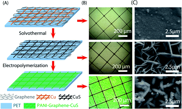
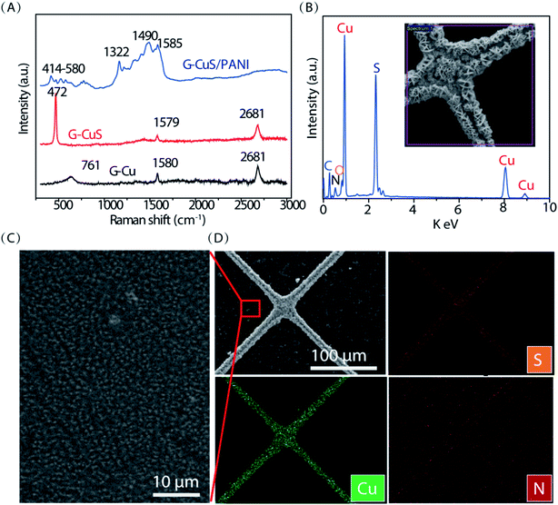
Fig. 1A schematically presents the processes of the synthesis of G–CuS/PANI on polyethylene terephthalate (PET) substrate through solvothermal reaction and electropolymerization. Firstly, Cu networks were converted into CuS networks by immersing G–Cu into an ethanol solution containing 0.6 g L−1 sulfur. By using this simple solvothermal method, we can easily obtain a large-scale flexible G–CuS TCE (Fig. S1 in the ESI†). It follows the microscope photographs in Fig. 1B that no obvious changes were observed in the morphology after the Cu networks were converted into CuS networks. The girds of the networks have a square configuration with the 300 μm length of the side (L) and the 10 μm width of the grid line (w). Corresponding SEM morphology images shown in Fig. 1C present that smooth Cu grid had been transformed into sheet-like CuS grid with the sheet thickness of ∼50 nm. Secondly, PANI was electrodeposited on G–CuS TCE by the electropolymerization method at a current density of 0.1 mA cm−2. It follows the micrograph in Fig. 1B that the whole TCE was uniformly coated by a green film. The corresponding SEM images for the green film on grid line and empty area are displayed in Fig. 1C and 2C, respectively, indicating the whole TCE was uniformly coated by a layer of PANI nanorods arrays with a diameter of ∼50 nm.The components of G–Cu, G–CuS and G–CuS/PANI were investigated by Raman analysis in Fig. 2A. The two typical peaks of graphene located at ∼1580 cm−1 and 2681 cm−1 can be readily indexed to the in-plane bond stretching motion of C sp2 atoms (G band) and the inter-valley double resonance Raman scattering (G′ band), respectively.41 In contrast to the G–Cu networks, the Raman spectrum of the CuS nanostructures showed a distinct band at 472 cm−1, which originates from the lattice S–S stretching of covellite.42 After deposition of PANI, several weak Raman peaks located at 414–580, 1322, 1490, and 1585 cm−1 emerged in the spectrum which are attributed to the out-of-plane C–N–C torsion, C–N+ stretching, C![[double bond, length as m-dash]](https://www.rsc.org/images/entities/char_e001.gif) N stretching of quinoid, and C–C stretching of benzenoid in PANI, respectively. Furthermore, energy dispersive X-ray spectroscopy (EDS) spectrum of G–CuS/PANI is displayed in Fig. 2B. The weak peak located at 0.38 eV is corresponding to the N element which belongs to PANI, which is consistent with the result of EDS mapping in Fig. 2D. Thanks to the wrapped graphene layer, PANI was not only polymerized on the surface of CuS grids, but also uniformly covered the entire G–CuS surface including the empty area as shown in Fig. 2D. On the contrary, PANI was only deposited on the CuS grids when we removed the wrapped graphene film (see Fig. S2 in the ESI†). The covered graphene plays an important role to increase the electronic distribution uniformity in the electrochemical polymerization process, and it is the PANI in the empty area that dominantly causes color changes of the supercapacitor.38
N stretching of quinoid, and C–C stretching of benzenoid in PANI, respectively. Furthermore, energy dispersive X-ray spectroscopy (EDS) spectrum of G–CuS/PANI is displayed in Fig. 2B. The weak peak located at 0.38 eV is corresponding to the N element which belongs to PANI, which is consistent with the result of EDS mapping in Fig. 2D. Thanks to the wrapped graphene layer, PANI was not only polymerized on the surface of CuS grids, but also uniformly covered the entire G–CuS surface including the empty area as shown in Fig. 2D. On the contrary, PANI was only deposited on the CuS grids when we removed the wrapped graphene film (see Fig. S2 in the ESI†). The covered graphene plays an important role to increase the electronic distribution uniformity in the electrochemical polymerization process, and it is the PANI in the empty area that dominantly causes color changes of the supercapacitor.38
Physicochemical properties of TCEs
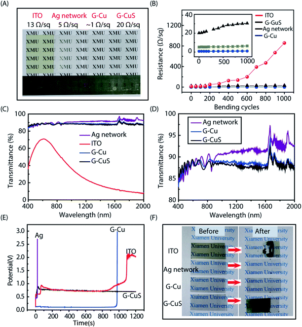
To investigate the physicochemical properties of the G–CuS network, three other TCEs including commercial ITO, G–Cu and Ag networks were introduced as references. Fig. 3A shows the photograph of the four different flexible TCEs, they were commercial ITO (13 Ω sq−1), (∼1 Ω sq−1), Ag network (5 Ω sq−1), and G–CuS (20 Ω sq−1), respectively. To examine the mechanical flexibility of the four TCEs, each sample with a size of 3.5 cm × 5 cm was bent to the radium of 0.5 cm, and then released to the initial position for 1000 times. As can be seen from Fig. 3B, negligible changes in the resistance were observed for G–Cu, Ag networks and G–CuS networks, while ITO suffered from serious damage and its Rs increased sharply. The broad transmittance spectra of the aforementioned four TCEs are plotted in Fig. 3C and D. The transmittances of the Ag network, G–Cu and G–CuS are almost flat in the range of 400–2000 nm while that of ITO demonstrated a sharp decrease in the range of wavelength greater than 700 nm, indicating network TCEs can solve the low infrared transmittance problem for the ITO films. Apart from high infrared transmittance, network TCEs exhibit excellent optoelectronic performance. The average transmittances of visible lights of Ag network (5 Ω sq−1) and G–Cu (∼1 Ω sq−1) are about 88.3% and 88.1%, respectively, which are much better than that of ITO (13 Ω sq−1 at a maximum transmittance of 71%). According to the calculation from eqn (S1) and Fig. S3 in the ESI,† the optical transmittances of the network TCEs mainly depend upon the unpatterned area.35 Therefore, in this work, the light transmittance of the Cu networks should be 93.4% according to the L and w of the grid are 300 μm and 10 μm, respectively. The transmittance of G–Gu TCE (88.1%) exhibited slightly lower than that of Cu networks (93.4%) can be attributed to the wrapped graphene layer reduced the light transmittance. It is worth to note that negligible decrease in transmittance was observed after converting G–Cu networks into G–CuS networks, indicating the transparency of the CuS film can be significantly increased after making the continuous film into mesh structure.Chemical stability is another important feature for TCEs in ECDs. Fig. 3E shows chronopotentiometric curves obtained during the galvanostatic electropolymerization of PANI on the aforementioned four flexible TCEs in an aniline–H2SO4 aqueous solution. For G–CuS, it reached a maximum potential value of about 0.80 V in less than 80 s corresponding to the formation of PANI, then, the potential decreased slightly and remained stable when we further extending the polymerization time.43 As for ITO, the potential remained stable in the first 880 s and then sharply increased due to ITO shows poor chemical stability and strong sensitivity to corrosive salts and acids.44 For Ag network and G–Cu, the deposition potentials at the beginning were only 0.42 V and 0.12 V, which is attributed to their superior conductivity. However, their chemical stability was also poor and only remained stable for 20 s and 960 s, respectively. It should be noted that G–Cu exhibited higher chemical stability than Ag network due to the fact that the graphene can retard the metallic TCEs to some extent oxidation in erosion solution.20,45,46 Fig. 3F shows the corresponding photograph before and after deposition of PANI film, indicating that PANI can be only deposited on G–CuS TCE while almost no PANI was observed on the other three TCEs. The clearer SEM images as shown in Fig. S4 (see ESI†) displays that both the Ag networks and Cu grids corroded and were eventually fractured. As we know, the major barrier to commercialization of most of the metallic TCE is their poor chemical stability. As for the CuS material, we has also previously demonstrated that CuS shows excellent chemical stability when exposed to various conditions of thermal oxidation at 160 °C, humid air with 80% relative humidity at 85 °C, and H2O2 solution, respectively.47 G–CuS TCEs represent a new opportunity for emerging flexible electronics required working in hash conditions.
Characterizations of electrochromic–supercapacitive performance
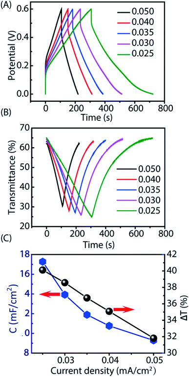
Based on the PANI electrodeposition results, we only chose G–CuS to further evaluate the possibility of its use as a TCE in the electrochromic supercapacitor. As we know, both electrochromic and supercapacitive behaviors of PANI are attributed to the redox reaction in the same acid electrolyte.48 In this context, we can simultaneously develop a multifunctional electrochromic supercapacitor that is capable of energy storage and transmittance adjustment. To evaluate the performance of the G–CuS/PANI film as an electrochromic-supercapacitor electrode, the charge–discharge curves at different current densities (Fig. 4A) and corresponding in situ transmittance at 620 nm (Fig. 4B) were tested. As can be seen from Fig. 4A, both the charging and discharging time increased while decreasing charge–discharge current densities from 0.050 mA cm−2 to 0.025 mA cm−2. As shown in Fig. 4B, the coloring process resulted in decreasing the transmittance while the bleaching process was just the reverse. According to the Fig. 4A and B, the variation of area capacitance (C) and optical modulation (ΔT) as function of current densities can be calculated and corresponding curves were displayed in Fig. 4C. It is obvious that C and ΔT decreased gradually with increasing the current density. It could be attributed the fact that the migration of the electroactive ions is limited to access inner surface of the active material for energy storage owing to the diffusion effect at high current density.38 It follows from Fig. 4C that G–CuS/PANI exhibited area capacitances of 17.3, 13.9, 11.9, 10.8 and 9.3 mF cm−2 at 0.025, 0.030, 0.035, 0.040 and 0.050 mA cm−2, along with optical modulation of 40.1%, 38.6%, 36.7%, 35.1% and 31.8%, respectively. In addition, C and ΔT at a high current density of 0.050 mA cm−2 sustained 54% and 79%, respectively, compared to the values at a low current density of 0.025 mA cm−2. The supercapacitive results of our work is comparable to that with the PEDOT/PET as the transparent conductive electrode, which is from 6 to 15 mF cm−2 when at the current density from 0.3 to 0.01 mA cm−2.17 And after galvanostatic charge–discharge tests for 200 cycles at a current density of 0.045 mA cm−2 as shown in Fig. S5 in the ESI,† G–CuS/PANI displayed a favorable cyclic stability with a decay of only 24% compared to its initial area capacitance. Furthermore, the corresponding IR drops at different current densities were displayed in Fig. S6 in the ESI.† The IR drop is generally attributed to the charge–discharge current density besides the electrolyte potential drop and contact resistance.17 G–CuS/PANI showed low IR drops from 76.73 mV at 0.025 mA cm−2 to 148.87 mV at 0.050 mA cm−2. The aforementioned results demonstrate that the G–CuS/PANI electrode exhibited a supercapacitive performance and an exciting combination of the electrochromic and supercapacitive properties. Furthermore, we assembled a symmetrical supercapacitor with H2SO4–PVA hydrogel as the electrolyte, which presented a excellent electrochromic response to the galvanostatic charge–discharge process as shown in Fig. 5. Its noticeable color variation enables users to intuitively evaluate the level of stored energy by naked eyes in a predictable manner.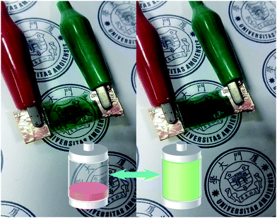 | ||
| Fig. 5 The color change of a supercapacitor responds to the level of stored energy during the charge–discharge process (a related movie has been provided in ESI,† Movie S1). | ||
Conclusions
In summary, a newly designed G–CuS TCE with high transparency, flexibility and conductivity has been fabricated by photolithography, chemical vapor deposition and a low-temperature solvothermal reaction. This novel TCE achieves an Rs of ∼20 Ω sq−1 with a transmittance of over 85%. During the bending test, G–CuS exhibited remarkable mechanical stability with a small Rs increase of ∼10 Ω sq−1 after 1000 bending cycles. Uniform PANI was successfully deposited on the G–CuS film by the galvanostatic electrodeposition in aniline–H2SO4 solution. The PANI/G–CuS electrode exhibited an excellent electrochromic supercapacitive performance, which achieved an area capacitance of 17.3 mF cm−2 along with a large optical modulation of 40.1%. Furthermore, a symmetrical supercapacitor was assembled in which the electrochromic property can intuitively reflect the condition of energy storage for visual assessment. The G–CuS TCE with excellent conductivity, transparency, mechanical stability and chemical stability will have a promising future in the flexible electronics. This work may supply an inspiration to the design of TCEs for electrochromic supercapacitors.Acknowledgements
This work was supported by Beijing Natural Science Foundation (2164076), the National Nature Science Foundation of China (No. 515022553, No. U1405226), Guangdong Natural Science Foundation (2016A030310369); the Fundamental Research Funds for the Central Universities of China (No. 20720150030), the “111” Project (B16029), Fujian Provincial Bureau of Science & Technology (2014H6022) and the 1000 Talents Program from Xiamen University.References
- M. Salanne, B. Rotenberg, K. Naoi, K. Kaneko, P. L. Taberna, C. P. Grey, B. Dunn and P. Simon, Nat. Energy, 2016, 1, 16070 CrossRef CAS.
- W. Li, J. Liu and D. Zhao, Nat. Rev. Mater., 2016, 1, 16023 CrossRef CAS.
- P. Simon and Y. Gogotsi, Nat. Mater., 2008, 7, 845–854 CrossRef CAS PubMed.
- P. Yang, P. Sun and W. Mai, Mater. Today, 2015, 19, 394–402 CrossRef.
- G. Cai, X. Wang, M. Cui, P. Darmawan, J. Wang, A. L.-S. Eh and P. S. Lee, Nano Energy, 2015, 12, 258–267 CrossRef CAS.
- Y. Tian, S. Cong, W. Su, H. Chen, Q. Li, F. Geng and Z. Zhao, Nano Lett., 2014, 14, 2150–2156 CrossRef CAS PubMed.
- D. Wei, M. R. Scherer, C. Bower, P. Andrew, T. Ryhänen and U. Steiner, Nano Lett., 2012, 12, 1857–1862 CrossRef CAS PubMed.
- X. Chen, H. Lin, P. Chen, G. Guan, J. Deng and H. Peng, Adv. Mater., 2014, 26, 4444–4449 CrossRef CAS PubMed.
- X. Chen, H. Lin, J. Deng, Y. Zhang, X. Sun, P. Chen, X. Fang, Z. Zhang, G. Guan and H. Peng, Adv. Mater., 2014, 26, 8126–8132 CrossRef CAS PubMed.
- W. Liu, M. S. Song, B. Kong and Y. Cui, Adv. Mater., 2017, 29, 1603436 CrossRef PubMed.
- M. Nikolou, A. L. Dyer, T. T. Steckler, E. P. Donoghue, Z. Wu, N. C. Heston, A. G. Rinzler, D. B. Tanner and J. R. Reynolds, Chem. Mater., 2009, 21, 5539–5547 CrossRef CAS.
- L. Hu, G. Gruner, D. Li, R. B. Kaner and J. Cech, J. Appl. Phys., 2007, 101, 016102 CrossRef.
- J. H. Lee, D. W. Shin, V. G. Makotchenko, A. S. Nazarov, V. E. Fedorov, Y. H. Kim, J.-Y. Choi, J. M. Kim and J.-B. Yoo, Adv. Mater., 2009, 21, 4383–4387 CrossRef CAS PubMed.
- W. R. Lian, Y. C. Huang, Y. A. Liao, K. L. Wang, L. J. Li, C. Y. Su, D. J. Liaw, K. R. Lee and J. Y. Lai, Macromolecules, 2011, 44, 9550–9555 CrossRef CAS.
- C. Sachse, N. Weiß, N. Gaponik, L. Müller-Meskamp, A. Eychmüller and K. Leo, Adv. Energy Mater., 2014, 4, 1300737 CrossRef.
- C. Lee, C. Kim, M. Jeong, J. Kim, J. Lee, J. W. Oh, J. Lee, S. H. Kim, S. S. Park and J. M. Kim, RSC Adv., 2015, 5, 77288–77295 RSC.
- K. Wang, H. Wu, Y. Meng, Y. Zhang and Z. Wei, Energy Environ. Sci., 2012, 5, 8384–8389 CAS.
- K. Sanglee, S. Chuangchote, P. Chaiwiwatworakul and P. Kumnorkaew, J. Nanomater., 2017, 2017, 8 Search PubMed.
- B. W. An, B. G. Hyun, S.-Y. Kim, M. Kim, M.-S. Lee, K. Lee, J. B. Koo, H. Y. Chu, B.-S. Bae and J.-U. Park, Nano Lett., 2014, 14, 6322–6328 CrossRef CAS PubMed.
- Y. Ahn, Y. Jeong, D. Lee and Y. Lee, ACS Nano, 2015, 9, 3125–3133 CrossRef CAS PubMed.
- Y. H. Kim, L. Müller-Meskamp and K. Leo, Adv. Energy Mater., 2015, 5, 1401822 CrossRef.
- S. K. Balasingam, M. Lee, B. H. Kim, J. S. Lee and Y. Jun, Dalton Trans., 2017, 46, 2122–2128 RSC.
- X. Li, W. Li, M. Li, P. Cui, D. Chen, T. Gengenbach, L. Chu, H. Liu and G. Song, J. Mater. Chem. A, 2015, 3, 2762–2769 CAS.
- B. M. Gray, A. L. Hector, M. Jura, J. R. Owen and J. Whittam, J. Mater. Chem. A, 2017, 5, 4550–4559 CAS.
- W. Li, C. Y. Cao, C. Q. Chen, Y. Zhao, W. G. Song and L. Jiang, Chem. Commun., 2011, 47, 3619–3621 RSC.
- W. Li, X. Gao, D. Xiong, F. Xia, J. Liu, W. G. Song, J. Xu, S. M. Thalluri, M. F. Cerqueira, X. Fu and L. Liu, Chem. Sci., 2017, 8, 2952–2958 RSC.
- Z. Zhang, S. Liu, J. Xiao and S. Wang, J. Mater. Chem. A, 2016, 4, 9691–9699 CAS.
- W. Li, X. Gao, X. Wang, D. Xiong, P.-P. Huang, W.-G. Song, X. Bao and L. Liu, J. Power Sources, 2016, 330, 156–166 CrossRef CAS.
- A. Cuevas, R. Romero, D. Leinen, E. A. Dalchiele, J. R. Ramos-Barrado and F. Martin, Sol. Energy Mater. Sol. Cells, 2015, 134, 199–208 CrossRef CAS.
- S. V. Bagul, S. D. Chavhan and R. Sharma, J. Phys. Chem. Solids, 2007, 68, 1623–1629 CrossRef CAS.
- P. Parreira, G. Lavareda, J. Valente, F. T. Nunes, A. Amaral and C. N. de Carvalho, Phys. Status Solidi A, 2010, 207, 1652–1654 CrossRef CAS.
- P. Parreira, G. Lavareda, A. Amaral, A. M. Botelho do Rego, O. Conde, J. Valente, F. Nunes and C. Nunes de Carvalho, J. Alloys Compd., 2011, 509, 5099–5104 CrossRef CAS.
- K. D. Yuan, J. J. Wu, M. L. Liu, L. L. Zhang, F. F. Xu, L. D. Chen and F. Q. Huang, Appl. Phys. Lett., 2008, 93, 132106 CrossRef.
- N. Fukaya, D. Y. Kim, S. Kishimoto, S. Noda and Y. Ohno, ACS Nano, 2014, 8, 3285–3293 CrossRef CAS PubMed.
- B. Y. Ahn, D. J. Lorang and J. A. Lewis, Nanoscale, 2011, 3, 2700–2702 RSC.
- Z. Xu, T. Li, F. Zhang, X. Hong, S. Xie, M. Ye, W. Guo and X. Liu, Nanoscale, 2017, 9, 3826–3833 RSC.
- Y. Zhu, Z. Sun, Z. Yan, Z. Jin and J. M. Tour, ACS Nano, 2011, 5, 6472–6479 CrossRef CAS PubMed.
- G. Cai, P. Darmawan, M. Cui, J. Wang, J. Chen, S. Magdassi and P. S. Lee, Adv. Energy Mater., 2016, 6, 1501882 CrossRef.
- X. M. Wu, W. Z. Zhang, Q. G. Wang, Y. Wang, H. Y. Yan and W. X. Chen, Synth. Met., 2016, 212, 1–11 CrossRef CAS.
- W. Ke, G. Fang, H. Lei, P. Qin, H. Tao, W. Zeng, J. Wang and X. Zhao, J. Power Sources, 2014, 248, 809–815 CrossRef CAS.
- L. M. Malard, M. A. Pimenta, G. Dresselhaus and M. S. Dresselhaus, Phys. Rep., 2009, 473, 51–87 CrossRef CAS.
- Y. Du, Z. Yin, J. Zhu, X. Huang, X.-J. Wu, Z. Zeng, Q. Yan and H. Zhang, Nat. Commun., 2012, 3, 1177 CrossRef PubMed.
- J. Yang and D. C. Martin, Sens. Actuators, B, 2004, 101, 133–142 CrossRef CAS.
- S. W. Gaarenstroom, M. P. Balogh, M. C. Militello, R. A. Waldo, C. A. Wong, N. A. Kelly, T. L. Gibson and M. D. Kundrat, Surf. Interface Anal., 2005, 37, 385–392 CrossRef CAS.
- W. Wu, N. G. Tassi, D. J. Walls, L. Zhang and B. Willner, Appl. Phys. Lett., 2014, 105, 223104 CrossRef.
- R. Mehta, S. Chugh and Z. Chen, Nano Lett., 2015, 15, 2024–2030 CrossRef CAS PubMed.
- X. Zhang, W. Guo, G. Gao, M. Que, C. Pan and Z. L. Wang, J. Mater. Chem. C, 2016, 4, 4733–4739 RSC.
- X. Xiang, W. Zhang, Z. Yang, Y. Zhang, H. Zhang, H. Zhang, H. Guo, X. Zhang and Q. Li, RSC Adv., 2016, 6, 24946–24951 RSC.
Footnotes |
| † Electronic supplementary information (ESI) available. See DOI: 10.1039/c7ra04476c |
| ‡ Authors contributed equally to this work. |
| This journal is © The Royal Society of Chemistry 2017 |

