
 Open Access Article
 This Open Access Article is licensed under a
 Creative Commons Attribution 3.0 Unported Licence
Ordered multiferroic CoFe2O4–Pb(Zr0.52Ti0.48)O3 coaxial nanotube arrays with enhanced magnetoelectric coupling
Dan Tang a,
Zhiqiang Zenga,
Qingwei Zhoud,
Shaoqiang Sua,
Die Hua,
Peilian Lia,
Xiaozi Lina,
Xingsen Gaoa,
Xubing Lua,
Xin Wangbc,
Mingliang Jinbc,
Guofu Zhoubc,
Zhang Zhang*ac and
Junming Liuad
a,
Zhiqiang Zenga,
Qingwei Zhoud,
Shaoqiang Sua,
Die Hua,
Peilian Lia,
Xiaozi Lina,
Xingsen Gaoa,
Xubing Lua,
Xin Wangbc,
Mingliang Jinbc,
Guofu Zhoubc,
Zhang Zhang*ac and
Junming Liuad
aInstitute for Advanced Materials, South China Academy of Advanced Optoelectronics, South China Normal University, Guangzhou 510006, People's Republic of China. E-mail: zzhang@scnu.edu.cn
bInstitute of Electronic Paper Display, South China Academy of Advanced Optoelectronics, South China Normal University, Guangzhou 510006, People's Republic of China
cInternational Academy of Optoelectronics at Zhaoqing, South China Normal University, Zhaoqing, Guangdong Province, China
dLaboratory of Solid State Microstructures, Innovation Center of Advanced Microstructures, Nanjing University, Nanjing 210093, People's Republic of China
First published on 2nd June 2017
Abstract
In this paper, vertically free-standing multiferroic CoFe2O4–Pb(Zr0.52Ti0.48)O3 (CFO–PZT) coaxial nanotube arrays with both good ordering and high density were prepared by a template-assisted sol–gel method. X-ray diffraction (XRD) and Raman spectra confirmed that the as-prepared CFO–PZT nanotubes (NTs) included both spinel CFO and perovskite PZT phases. The multiferroic properties were demonstrated by magnetic hysteresis and piezo-response force microscopy (PFM). We also observed an effective dielectric constant of about 0.8% between increasing and decreasing magnetic field, indicating that the ordered CFO–PZT coaxial nanotube arrays may enable potential high-density magnetoelectric (ME) devices.
Introduction
Multiferroic magnetoelectric (ME) materials can display both electric and magnetic order simultaneously, which opens up a new avenue for novel complexity devices, such as ME sensors, actuators and logical devices, as well as low power consumption and high density ME memorizers.1–5 However, the single-phase ME materials are relatively rare and the corresponding ME responses are either extremely weak or occur only at low temperatures.6 In order to enhance the ME coupling for practical applications, most multiferroic materials are in composite forms with a combination of ferroelectric perovskites and ferromagnetic spinels.7–9Up to the present time, various multiferroic composites have been deeply investigated. For instance, the (2-2) laminate composites, (1-3) columnar films, (0-3) particulate composites, as well as core–shell nanotube/nanofiber composites.10–16 The (2-2) laminate composites can be obtained via a layer-by-layer deposition, which can provide a near-perfect mechanical coupling. Yet, for the clamping from the substrates, the ME response of these multilayers was limited to quite a low level.17 The (1-3) columnar films can be obtained during the spontaneous phase separation (involving one composite target), which greatly enhanced the ME coupling, enabling an electric-field induced magnetization switching.15,18 Nevertheless, owing to the low resistivity of conductive interfaces or the constitutional magnetic phases, the (1-3) columnar films were exposed to a large leakage current.19 Other structures like (0-3) particulate composites had been reported to have a clamping effect improvement (better than the (2-2) type) and a leakage current reduction (better than the (1-3) structure).20,21 However, it is still difficult to control the distribution of magnetic phase component due to its self-assembly nature, and the fabrication process is also quite complicated.22 In addition, one-dimensional (1D) core–shell nanotube/nanofiber may offer several advantages. First, coaxial 1D nanocomposites can provide larger interfacial contact than the thin film multilayers which display both heteroepitaxy and significant strain effects. Moreover, the coaxial 1D nanocomposites exhibit a low leakage current and a higher order ME coupling.22 Recent theoretical analysis also indicated that the multiferroic 1D nanocomposites had exhibited ME responses orders of magnitude higher than that of the similar compositions, due to their substantially relaxed substrate constraint.23 Moreover, it is with the possibility to diminish the mutual influence between the neighboring nanocomposites.
So far, in order to explore the ME coupling, numerous efforts have been made in the synthesis of 1D multiferroic coaxial nanotube/nanofiber. Xie et al. realized the multiferroic CFO–PZT core–shell nanofibers through a coaxial electrospinning sol–gel process, of which the lateral ME coefficient was two orders of magnitude higher than that of the thin films.16 Sun et al. used the similar method to fabricate Ni/P(VDF-TrFE) coaxial cables, which improved the dielectric property and enhanced the ferroelectric polarization.24 By the template-assisted sol–gel method, the magnetoelectric coaxial CFO–PZT and CFO–BTO NTs could be prepared, which were both lack of the presentation of the magnetoelectric coupling effect.25,26 Obviously, the templates around the nanostructures would induce the clamping effect and degrade the magnetic as well as electronic properties.27–29 However, without the mechanical support from template, the existences of capillary force and surface tension always result in the degradation of arrays alignment on the substrate.30,31 As a trade-off solution, the high density nanostructures should be preferentially designed with a low aspect ratio of height to diameter.32 In general, CFO has been widely adopted to construct composite multiferroics, for its good magnetic property, low conductivity, and large magneto-restriction. PZT, as the other composition, exhibits excellent ferroelectric and piezoelectric properties. The combination of the two components in an ordered free-standing coaxial nanotube arrays could be potentially applied in future micro/nano-ME devices.
In this work, we present the high density and ordered free-standing CFO–PZT coaxial nanotube arrays by a template-assisted sol–gel method. The morphologies, crystalline structures, as well as the multiferroic properties had been studied. We found that, the degree of clamping effect from the template was mostly removed in the free-standing nanostructure. The stress state of the free-standing coaxial CFO–PZT NTs was further studied by means of Raman spectroscopy. Through magnetocapacitance measurements, we have also discussed the existence of ME coupling effect in the nanostructures, which opened up opportunities for the potential high-density ME devices.
Experimental section
Templates fabrication
Templates of anodic aluminum oxides (AAO) were fabricated by a standard two-step anodization method.33,34 First, high-purity aluminum foils (99.999%, Good Fellow Cambridge Limited) were degreased, and then annealed at 450 °C for 3 h under argon (Ar) atmosphere. Then, the Al foils were electrochemically polished in a solution of ethanol and HClO4 (3![[thin space (1/6-em)]](https://www.rsc.org/images/entities/char_2009.gif) :1 by volume) at 20 V for 5 min. The first anodic oxidation process was performed in a 0.3 M oxalic acid with a constant anodic voltage of 40 V. After 24 h, the first alumina layer was removed off by an aqueous solution of 6% H3PO4 and 1.8% H2CrO4 at 45 °C for 11 h. The second anodic oxidation process was performed under the same conditions as the first one, with a 300 s oxidation period to form the AAO membrane with a thickness of about 200 nm. Then, a 5 wt% phosphoric acid was used to widen the pore diameter to about 80 nm. A polymer-assisted method was used to realize the AAO membrane bonding onto Pt/Si substrate.27 First, a thin layer of polystyrene (PS) (1 wt% PS/CHCl3 solution) was spin coated onto the top of AAO membrane, followed by a 90 °C solidification heating. After that, a CuCl2 solution (6.8 g CuCl2 + 100 ml 37% HCl + 200 ml distilled water) was used to remove the Al foil on the back side of the AAO. The detached AAO membrane was transferred onto a 5 wt% phosphoric acid at 35 °C for 30 min, rinsed with distilled water, and then dried under ambient conditions to remove the barrier layer.35 The PS/AAO membrane floating on the surface of deionized water was transferred to a desired substrate. Finally, the PS can be completely removed by a pyrolysis process.
:1 by volume) at 20 V for 5 min. The first anodic oxidation process was performed in a 0.3 M oxalic acid with a constant anodic voltage of 40 V. After 24 h, the first alumina layer was removed off by an aqueous solution of 6% H3PO4 and 1.8% H2CrO4 at 45 °C for 11 h. The second anodic oxidation process was performed under the same conditions as the first one, with a 300 s oxidation period to form the AAO membrane with a thickness of about 200 nm. Then, a 5 wt% phosphoric acid was used to widen the pore diameter to about 80 nm. A polymer-assisted method was used to realize the AAO membrane bonding onto Pt/Si substrate.27 First, a thin layer of polystyrene (PS) (1 wt% PS/CHCl3 solution) was spin coated onto the top of AAO membrane, followed by a 90 °C solidification heating. After that, a CuCl2 solution (6.8 g CuCl2 + 100 ml 37% HCl + 200 ml distilled water) was used to remove the Al foil on the back side of the AAO. The detached AAO membrane was transferred onto a 5 wt% phosphoric acid at 35 °C for 30 min, rinsed with distilled water, and then dried under ambient conditions to remove the barrier layer.35 The PS/AAO membrane floating on the surface of deionized water was transferred to a desired substrate. Finally, the PS can be completely removed by a pyrolysis process.
Fabrication of coaxial CFO–PZT NTs
A 0.3 M PZT sol–gel precursor with the molar ratio of 1:0.52:0.48 was prepared by dissolving zirconium propoxide (Zr(CH2CH2CH3O)4) and isopropyl titanate (Ti(C4H9O)4) into 2-methoxyethanol (C3H8O2), with acetic acid and propanol added as the solvents, stirring until completely dissolved. Then, a 10% excess lead acetate trihydrate (Pb(CH3CO2)2·3H2O) was added for the purpose of compensating the lead loss and preventing forming the second phase of pyrochlore-type in annealing process.36 The CFO sol–gel solution was prepared by mixing cobalt acetate, ferric nitrate, and polyvinylpyrrolidone together at 60 °C, according to the molar ratio of 1:2:2, until a clear solution was obtained. Then, the 2-methoxyethanol was added to obtain 0.5 M of CFO sol–gel solution. The pH value of the resultant dark-red CFO sol–gel solution was 4.2.37 The precursor solutions were stirred for 24 h at room temperature and then aged for 1 week.
The synthesis of coaxial CFO–PZT NTs consists of two steps. First, the AAO template was dipped into PZT sol for nearly 10 h at room temperature. After the infiltration process, excessive PZT accumulated on the surface was swept with high-pressure N2. The samples were then annealed at 700 °C for 20 min in air by a rapid thermal process (RTP) to experience a crystallization process. Afterwards, under a pressure of 5.6 × 10⁻⁴ mbar at room temperature, the specimen was etched in an Ar gas IBE system (MIBE-150C). The etching energy was set to a cathode current of 11.5 A, anode voltage of 55 V, plate voltage of 300 V, ion accelerating voltage of 250 V, neutralization current of 13 A and bias current of 1.2 A.27 The first 10 min IBE was used to remove off the residual PZT film that covered on the top surface of AAO after the annealing process. The continuous IBE reduced both the thicknesses of AAO and PZT inside the pores. The total etching time was about 20 min with a vertical incident ion beam to the specimen. Second, to realize the coaxial nanostructure, the PZT NTs together with AAO template was dipped into the CFO sol for about 8 h. The consecutive annealing and IBE processes were the same as those for PZT. The remaining AAO was completely removed off by dipping the specimen into sodium hydroxide solution. For comparison, PZT NTs and CFO NTs were also fabricated by the AAO template-assisted method, respectively.
Characterizations
The nanostructure morphologies were carried out ex situ by a field-emission scanning electron microscope (FESEM ZEISS Ultra 55). The crystalline structural characterizations were investigated by XRD with an X-ray wavelength of 0.15406 nm. The Raman spectra were measured at room temperature by a microscopy Raman spectrometer (Renishaw 42K864) with an excitation wavelength of 633 nm, the laser power is set to 10% of its maximum. The ferroelectric nanostructures were measured by a piezo-response force microscopy (PFM) (Cypher, Asylum Research). The magnetization loop measurement was conducted by a vibrating sample magnetometer (VSM) imbedded inside a physical property measurement system (PPMS-9, Quantum Design). For the magnetocapacitance measurement, an Agilent 4990A LCR meter was used to measure the dielectric signal, while a Quantum Design PPMS provided the variable magnetic field.Results and discussion
The fabrication of ordered coaxial CFO–PZT nanotube arrays by a template-assisted sol–gel method was schematically illustrated in Fig. 1. First, a conductive Pt/Si substrate with bonded AAO membrane was dipped into the PZT sol. After the annealing, the presence of PZT film absorbed on the top surface of AAO would prevent the infiltration of CFO precursor and the selectively chemical etching of AAO. Therefore, by the IBE, the redundant PZT on the top surface of AAO was removed off. Subsequently, the PZT filled AAO was dipped into the CFO sol. After the annealing, the coaxial CFO–PZT NTs were formed inside the AAO pores. By the second IBE, besides the redundant CFO being removed off, both the heights of AAO and the embedded CFO–PZT NTs were reduced as well. Finally, by a selectively chemical etching of AAO, the ordered vertically free-standing coaxial CFO–PZT nanotube arrays were remained on the substrate.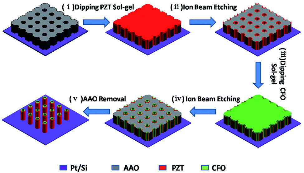 | ||
| Fig. 1 Schematic diagram showing the fabrication procedures of ordered vertically free-standing CFO–PZT coaxial nanotube arrays on Pt/Si substrate. | ||
The top-view SEM images of different fabrication procedures were present in Fig. 2. Before the AAO being transferred to a Pt/Si substrate, the barrier layer at the bottom side was selectively etched off by a chemical solution. Meanwhile, such a treatment introduced the pore widening from 40 to 80 nm as well (as shown in Fig. 2a). Due to the capillary effect, the PZT sol could be filled into the pores of AAO.38 After the infiltration process, the PZT inside AAO was annealed in air by a RTP. During the IBE, the neutral-charged Ar ion beam can transmit its kinetic energy to the atoms of the specimen to sputter out. And the high-energized Ar ion beam also play as a dustman to clean the sputtering re-deposition on surfaces to speed up the etching process.27,39 After a proper duration of IBE, the top PZT layer was completely removed off, and the ring-like PZT layer could be distinguished (as shown in Fig. 2b), being tightly embedded in AAO pores with an average wall thickness about 20 nm. Afterwards, the sample was dipped into the CFO sol. Due to the chemical affinity between polar molecules, the inner CFO layer could be formed inside the PZT NTs. After the IBE process, the embedded CFO–PZT coaxial double-layer nanostructures were exposed (as shown in Fig. 2c), with an average wall thickness about 30 nm. Compared the two top-view images, the thickness of the inner CFO layer is about 10 nm. After the AAO template being selectively removed off, as shown in Fig. 2d, the vertically free-standing CFO–PZT coaxial NTs were recognized from the top-view SEM image. Obviously, the two components could be distinguished with a contrast difference in Fig. 2d. Therefore, by the template assisted sol–gel method, CFO–PZT coaxial nanotube arrays with a high density and good ordering were realized.
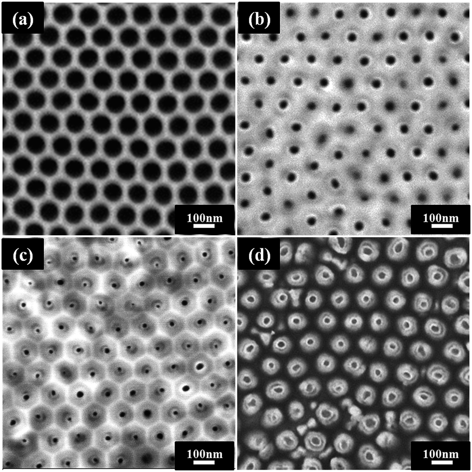 | ||
| Fig. 2 Top-view SEM images of the fabrication procedures of CFO–PZT coaxial nanotube arrays. (a) The pore-through AAO template with a mean diameter of about 80 nm and an inter-pore distance of 100 nm. (b) PZT and (c) CFO–PZT nanostructures inside the AAO templates after the IBE. (d) Vertically free-standing CFO–PZT coaxial nanotube arrays on Pt/Si substrate after selectively etching of AAO. | ||
As shown in Fig. 3a, the structural characterizations of PZT, CFO and CFO–PZT free-standing nanotube arrays with the same diameter were carried out by X-ray diffraction (XRD). The polycrystalline perovskite PZT and spinel CFO were confirmed by the XRD pattern, without additional or intermediate phase peaks.27,40 And the strongest two diffraction peaks corresponded to the PZT(110) and CFO(311) plane, respectively. As to the CFO–PZT coaxial NTs, the peaks were recognized all belonging to the perovskite PZT and the spinel CFO.
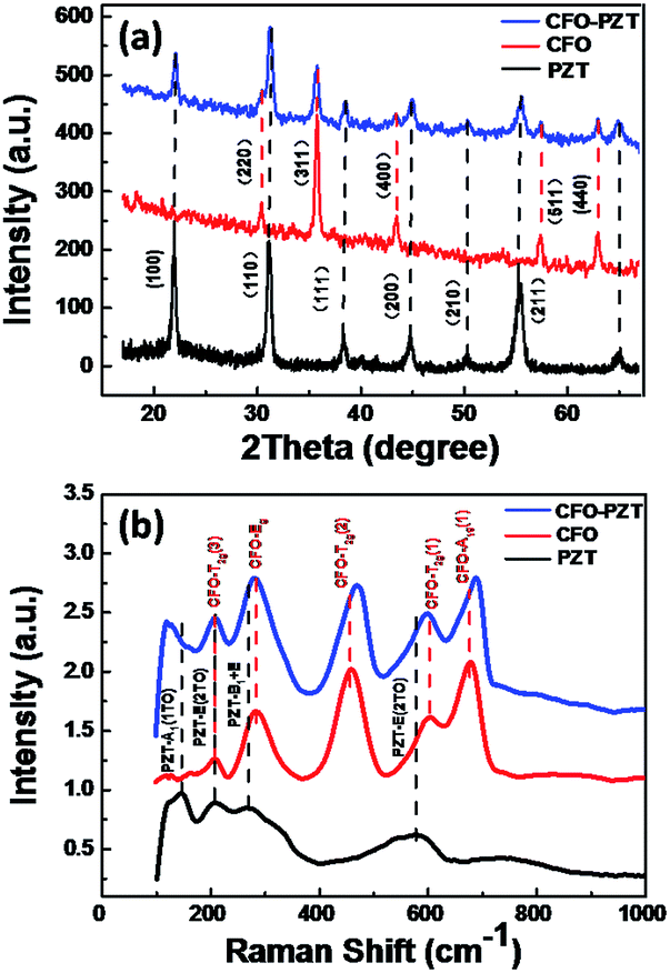 | ||
| Fig. 3 (a) XRD peak pattern of PZT, CFO and CFO–PZT free-standing nanotube arrays vertically aligned on Pt/Si (111) substrate, and (b) the corresponding Raman spectra measured at room temperature. | ||
To further characterize the composition and the stress state, the corresponding Raman spectra measured at room temperature were shown in Fig. 3b. The Raman peaks of pure PZT and CFO NTs were clearly observed, without additional or intermediate phase peaks.27,41,42 Since the PZT tetragonal space group belongs to the P4mm, the typical 3A1 + B1 + 4E mode in Raman peaks can be clearly identified. The four main peaks at 147, 208, 270, and 578 cm−1, correspond to the A1(1TO), E(1TO), E(silent) + B1, and A1(3TO) modes, respectively.27 For a cubic CFO spinel, Fd3m space group analysis yields 5 Raman modes of A1g + 3T2g + Eg.41 The Raman peaks of CFO at 208, 284, 459, 602, and 678 cm−1 correspond to the T2g(3), Eg, T2g(2), T2g(1), and A1g modes, respectively.42 Although the modes below 100 cm−1 were not recorded due to the equipment limitation, other active modes such as the soft-modes A1(1TO) and E(2TO) for the PZT layer and A1g mode for the CFO layer could be clearly distinguished.
By comparing the Raman spectra, we observed a high wave-number shift of about 9 cm−1 and 10 cm−1 for the A1g and T2g(2) vibration modes of CFO in the spectrum of CFO–PZT coaxial NTs, respectively. The shift of Raman peaks mainly arises from different residual stress statuses. As reported, a low wave-number shift of the vibration modes of CFO could be ascribed to the increase of out-of-plane tensile strain.43,44 Therefore, we assumed that the high wave-number shift had indicated the release of the out-of-plane tensile strain in the CFO layer of free-standing CFO–PZT coaxial NTs. Generally, the thermal effect and lattice mismatch are considered to be the two key factors for the residual stress.45 In the template-assisted sol–gel synthesis on a Pt/Si substrate, the thermal effect should determine the macroscopic residual stress in the NTs.
To characterize the ferroelectric properties of the ordered CFO–PZT coaxial nanotube arrays, PFM measurements were performed and demonstrated in Fig. 4. The surface topology (as shown in Fig. 4a) exhibited a closed-packed hexagonal ordering of arrays. The diameter of CFO–PZT NTs was about 80 nm, and the wall thickness of the PZT and CFO in CFO–PZT NTs was identified to be about 20 nm and 10 nm, respectively, being consistent with the SEM observation. The dark and bright areas in the phase micrograph of Fig. 4b corresponded to the up-polarization and down-polarization state, respectively, indicating the well-defined piezo-response of PZT in the ordered CFO–PZT nanotube arrays. The obvious contrasts in an amplitude piezo-response of Fig. 4c represent the magnitudes of the piezoelectric signals.
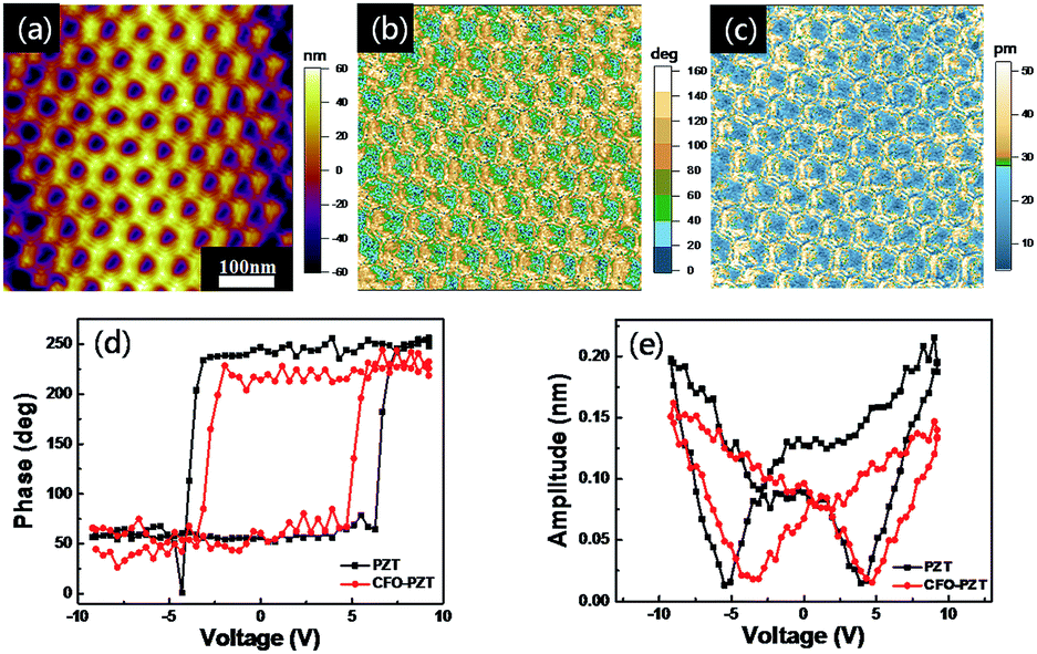 | ||
| Fig. 4 Piezoelectric response of the ordered CFO–PZT coaxial NTs on a Pt/Si substrate. (a) The surface topology, the corresponding (b) phase image and (c) amplitude image. The switching characteristics of piezo-response required by PFM (d) phase-voltage hysteresis loop and (e) amplitude–voltage butterfly loop coaxial nanotube arrays on Pt/Si substrate. | ||
Furthermore, to examine the local ferroelectric properties, the piezoelectric hysteresis loops on a single PZT nanotube and CFO–PZT coaxial nanotube were measured. The square-shaped phase-voltage piezo-response hysteresis loop and the butterfly-shaped amplitude–voltage loop were present in Fig. 4d and e. With the bias voltage increasing from −10 to +10 V, the phase change in PZT and CFO–PZT coaxial NTs was about 177° and 170° (Fig. 4d), respectively. Generally, such a phase change indicated that the low aspect ratio of nanostructures had resulted in an easier polarization switching.46 Meanwhile, a well-developed butterfly-shaped amplitude loop had been observed in Fig. 4e. The coercive fields of the PZT and CFO–PZT coaxial NTs were about −4.36 × 10² kV cm−1, +3.44 × 10² kV cm−1 and −2.87 × 10² kV cm−1, +3.98 × 10² kV cm−1, respectively. The asymmetric polarization reversal could be due to the built-in fields from the work-function difference between the top and bottom electrodes. The PFM conductive needle point as the top electrode was platinum iridium, while the bottom electrode was platinum silicon. Normally, the work function of platinum and the iridium is around 5.65 eV and 5.27 eV, respectively. Theoretically, it should produce an overall built-in voltage of 0.38 eV, which breaks the equivalence of two polarization states and provides a strong tendency to align the domains to a preferred orientation.8,47,48 Additionally, the surface charges stored at the interface between PZT and Pt electrode may contribute to the observed asymmetric polarization states.49 In the PZT NTs, the PFM amplitude coercive voltage is around 4 V. However, in the CFO–PZT coaxial NTs, the corresponding coercive voltage increased to 5 V. The internal stress on the interface between the CFO and PZT layers, making it harder for the switching of ferroelectric domains, could result in an increased coercive voltage and the smaller PFM amplitude.50–52
To confirm the multiferroicity, both ferromagnetism and ferroelectricity of the CFO–PZT coaxial NTs need to be verified. By a vibrating sample magnetometer (VSM), room temperature ferromagnetism of the vertically aligned free-standing CFO and CFO–PZT NTs with the same size and density were investigated, with the applied magnetic field parallel or perpendicular to the pillar axis. As shown in Fig. 5a, the CFO NTs have a saturated hysteresis loop with an in-plane magnetic coercive field Hc of 495 Oe, while the CFO–PZT NTs have an in-plane Hc of 615 Oe. Fig. 5b shows out-of-plane Hc of 621 Oe and 837 Oe for CFO and CFO–PZT NTs, respectively. Obviously, for both CFO and CFO–PZT NTs, the Hc along the in-plane direction is smaller than the one along out-of-plane direction. Such a phenomenon indicates that the magnetic easy axis is perpendicular to the substrate, which is consistent with the theoretical research.53 Since PZT is a typical ferroelectric material and has no magnetism, the magnetization of CFO–PZT coaxial NTs should arise from the inner CFO layer. The interface diffusion between CFO and PZT phases could make it harder for magnetic domains switching, resulting in a higher coercive field.16 Therefore, it is reasonable that the CFO–PZT coaxial NTs have a higher Hc than the CFO NTs in both directions. Meanwhile, the coercive field of CFO–PZT coaxial NTs is lower than 1 KOe, which had been measured from the PZT–CFO bilayered films.45
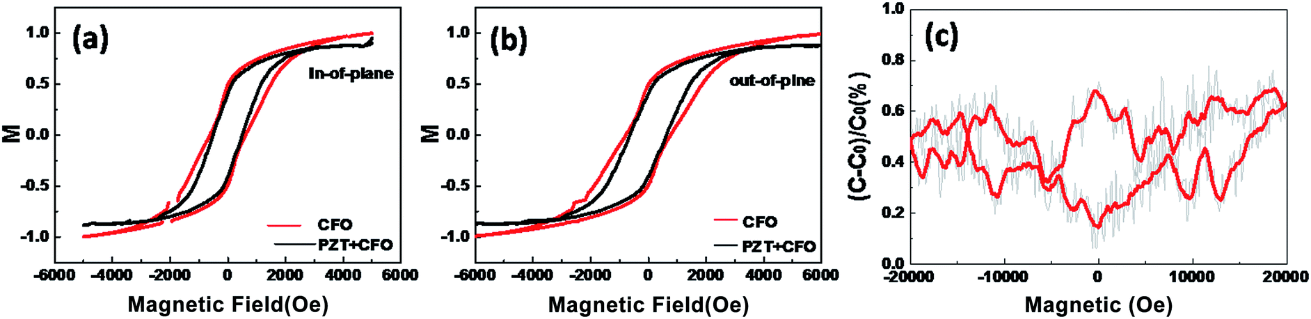 | ||
| Fig. 5 (a) In-plane magnetic hysteresis loops and (b) out-of-plane magnetic hysteresis loops of CFO and CFO–PZT NTs. (c) The magneto capacitance loop of CFO–PZT coaxial NTs measured at room temperature. | ||
The investigation for the ME coupling were performed at room temperature by a capacitance structure with Pt as a top electrode. Although a clearly linear ME coupling was not observed directly, we did find an evidence for magnetoelectric interaction through the magnetocapacitive measurements. Fig. 5c shows a room temperature magnetocapacitance plot, at a frequency of 30 kHz under a 0.1 V excitation capacitance, with both the magnetic and electric fields being parallel to the axis of CFO–PZT NTs. Hysteresis in the electrical properties of CFO inside PZT was shown by an applied magnetic field, with a change in the effective dielectric constant of about 0.8% between increasing and decreasing magnetic field. Although it is a relatively small change in dielectric constant, due to averaged signal of the capacitive measurements over a relatively large electrode, the intrinsic coupling may be larger than the measured one.22 The combination of magnetoelastic and piezoelectric effects through strain mediation and interface conductive may induce magneto-capacitance. The test frequency of magnetocapacitive measurement is beyond the space charge activation frequency, therefore the measured ME coupling may result from strain field transfer between the two phases.8 The observed hysteretic behavior of the magnetocapacitive coupling in such a system may have potential ME device applications.
Conclusions
In summary, ordered vertically free-standing multiferroic CFO–PZT coaxial nanotube arrays were realized by a template-assisted sol–gel method. The double-layer tubular nanostructure was confirmed by SEM. XRD and Raman spectrum had been performed to demonstrate the coexistence of spinel CFO and perovskite PZT phases in the CFO–PZT coaxial NTs. The observation of shifts in Raman phonon modes indicated the release of tensile strain without the template. Both the ferroelectricity and ferromagnetism of CFO–PZT coaxial NTs have been investigated. Furthermore, a higher order ME coupling in CFO–PZT coaxial NTs was revealed via the magnetocapacitance measurements, indicating the possible tenability of the dielectric permittivity with external magnetic field. Such ordered high-density multiferroic nanostructures could be potentially applied for new ME devices at nanoscale.Acknowledgements
We acknowledge the financial support by the National Science Foundation of China (Grant No. 51202072), the National Key Research and Development Program of China (2016YFB0401501), the State Key Program for Basic Researches of China (Grant No. 2015CB921202), Program for Changjiang Scholars and Innovative Research Team in University (Grant No. IRT13064), Guangdong Innovative Research Team Program (Grant No. 2011D039), Pearl River S&T Nova Program of Guangzhou (2105), Science and Technology Planning Project of Guangdong Province (Grant No. 2014B090914004 and No. 2015B090927006) and the 111 Project. The authors would also like to acknowledge Mr Guohui Lin for preparation of SEM samples.Notes and references
- J.-M. Hu, Z. Li, L.-Q. Chen and C.-W. Nan, Adv. Mater., 2012, 24, 2869 CrossRef CAS PubMed.
- J.-M. Hu, Z. Li, L.-Q. Chen and C.-W. Nan, Nat. Commun., 2011, 2, 553 CrossRef PubMed.
- U. Bauer, M. Przybylski, J. Kirschner and G. S. D. Beach, Nano Lett., 2012, 12, 1437 CrossRef CAS PubMed.
- D. S. Rana, I. Kawayama, K. Mavani, K. Takahashi, H. Murakami and M. Tonouchi, Adv. Mater., 2009, 21, 2881 CrossRef CAS.
- Y. Wang, J. Li and D. Viehland, Mater. Today, 2014, 17, 269 CrossRef CAS.
- N. A. Hill, J. Phys. Chem. B, 2000, 104, 6694 CrossRef CAS.
- H. Zheng, J. Wang, S. Lofland, Z. Ma, L. Mohaddes-Ardabili, T. Zhao, L. Salamanca-Riba, S. Shinde, S. Ogale and F. Bai, Science, 2004, 303, 661 CrossRef CAS PubMed.
- X. S. Gao, B. J. Rodriguez, L. F. Liu, B. Birajdar, D. Pantel, M. Ziese, M. Alexe and D. Hesse, ACS Nano, 2010, 4, 1099 CrossRef CAS PubMed.
- Q. Zhan, R. Yu, S. P. Crane, H. Zheng, C. Kisielowski and R. Ramesh, Appl. Phys. Lett., 2006, 89, 172902 CrossRef.
- H.-C. He, J. Wang, B.-P. Zhou and C.-W. Nan, Adv. Funct. Mater., 2007, 17, 1333 CrossRef CAS.
- M. Murakami, K. S. Chang, M. A. Aronova, C. L. Lin, M. H. Yu, J. H. Simpers, M. Wuttig, I. Takeuchi, C. Gao, B. Hu, S. E. Lofland, L. A. Knauss and L. A. Bendersky, Appl. Phys. Lett., 2005, 87, 112901 CrossRef.
- H. Zheng, J. Wang, S. E. Lofland, Z. Ma, L. Mohaddes-Ardabili, T. Zhao, L. Salamanca-Riba, S. R. Shinde, S. B. Ogale, F. Bai, D. Viehland, Y. Jia, D. G. Schlom, M. Wuttig, A. Roytburd and R. Ramesh, Science, 2004, 303, 661 CrossRef CAS PubMed.
- J. H. Park, H. M. Jang, H. S. Kim, C. G. Park and S. G. Lee, Appl. Phys. Lett., 2008, 92, 062908 CrossRef.
- S. M. Stratulat, X. Lu, A. Morelli, D. Hesse, W. Erfurth and M. Alexe, Nano Lett., 2013, 13, 3884 CrossRef CAS PubMed.
- N. M. Aimon, D. H. Kim, X. Sun and C. A. Ross, ACS Appl. Mater. Interfaces, 2015, 7, 2263 CAS.
- S. Xie, F. Ma, Y. Liu and J. Li, Nanoscale, 2011, 3, 3152 RSC.
- K. Lefki and G. J. M. Dormans, J. Appl. Phys., 1994, 76, 1764 CrossRef.
- F. Zavaliche, H. Zheng, L. Mohaddes-Ardabili, S. Y. Yang, Q. Zhan, P. Shafer, E. Reilly, R. Chopdekar, Y. Jia, P. Wright, D. G. Schlom, Y. Suzuki and R. Ramesh, Nano Lett., 2005, 5, 1793 CrossRef CAS PubMed.
- Y.-H. Hsieh, J.-M. Liou, B.-C. Huang, C.-W. Liang, Q. He, Q. Zhan, Y.-P. Chiu, Y.-C. Chen and Y.-H. Chu, Adv. Mater., 2012, 24, 4564 CrossRef CAS PubMed.
- Y. Li, Z. Wang, J. Yao, T. Yang, Z. Wang, J. M. Hu, C. Chen, R. Sun, Z. Tian, J. Li, L. Q. Chen and D. Viehland, Nat. Commun., 2015, 6, 6680 CrossRef CAS PubMed.
- L. Li, L. Lu, D. Zhang, R. Su, G. Yang, J. Zhai and Y. Yang, ACS Appl. Mater. Interfaces, 2015, 8, 442 Search PubMed.
- T. Narayanan, B. Mandal, A. Tyagi, A. Kumarasiri, X. Zhan, M. G. Hahm, M. Anantharaman, G. Lawes and P. Ajayan, Nano Lett., 2012, 12, 3025 CrossRef CAS PubMed.
- C. L. Zhang, W. Q. Chen, S. H. Xie, J. S. Yang and J. Y. Li, Appl. Phys. Lett., 2009, 94, 102907 CrossRef.
- C.-L. Sun, K. H. Lam, C. Chao, S. T. Lau, H. L. W. Chan, S. Guo and X. Zhao, Appl. Phys. Lett., 2007, 90, 253107 CrossRef.
- Z. Hua, P. Yang, H. Huang, J. Wan, Z.-Z. Yu, S. Yang, M. Lu, B. Gu and Y. Du, Mater. Chem. Phys., 2008, 107, 541 CrossRef CAS.
- K. Raidongia, A. Nag, A. Sundaresan and C. Rao, Appl. Phys. Lett., 2010, 97, 062904 CrossRef.
- X. Zhang, D. Tang, K. Huang, F. Zhang, X. Gao, X. Lu, G. Zhou, Z. Zhang and J. Liu, Nanoscale Res. Lett., 2016, 11, 1 CrossRef PubMed.
- F. Griggio, S. Jesse, A. Kumar, O. Ovchinnikov, H. Kim, T. N. Jackson, D. Damjanovic, S. V. Kalinin and S. Trolier-McKinstry, Phys. Rev. Lett., 2012, 108, 157604 CrossRef CAS PubMed.
- G. Lawes, A. P. Ramirez, C. M. Varma and M. A. Subramanian, Phys. Rev. Lett., 2003, 91, 257208 CrossRef CAS PubMed.
- T. Tanaka, M. Morigami and N. Atoda, J. Electrochem. Soc., 1993, 140, L115 CrossRef CAS.
- K. Zhu, T. B. Vinzant, N. R. Neale and A. J. Frank, Nano Lett., 2007, 7, 3739 CrossRef CAS PubMed.
- H. Namatsu, K. Kurihara, M. Nagase, K. Iwadate and K. Murase, Appl. Phys. Lett., 1995, 66, 2655 CrossRef CAS.
- Z. Zeng, Q. Zhou, Z. Yang, Q. Miao, G. Zhou and Z. Zhang, J. Nanosci. Nanotechnol., 2016, 16, 12231 CrossRef CAS.
- Z. Zeng, D. Tang, L. Liu, Y. Wang, Q. Zhou, S. Su, D. Hu, B. Han, M. Jin, X. Ao, R. Zhan, X. Gao, X. Liu, G. Zhou, S. Senz, Z. Zhang and J. Liu, Nanotechnology, 2016, 27, 12231 Search PubMed.
- C. Y. Han, G. A. Willing, Z. Xiao and H. H Wang, Langmuir, 2007, 23, 1564 CrossRef CAS PubMed.
- S. Tiwari and D. J. Frank, Appl. Phys. Lett., 1992, 60, 630 CrossRef CAS.
- W. Chen and W. Zhu, J. Am. Ceram. Soc., 2011, 94, 1096 CrossRef CAS.
- S. Singh and S. Krupanidhi, J. Nanosci. Nanotechnol., 2008, 8, 335 CAS.
- A. A. Tseng, J. Micromech. Microeng., 2004, 14, R15 CrossRef CAS.
- J. Wang, L. Wang, G. Liu, Z. Shen, Y. Lin and C. Nan, J. Am. Ceram. Soc., 2009, 92, 2654 CrossRef CAS.
- Z. Wang, R. T. Downs, V. Pischedda, R. Shetty, S. Saxena, C. Zha, Y. Zhao, D. Schiferl and A. Waskowska, Phys. Rev. B: Condens. Matter Mater. Phys., 2003, 68, 094101 CrossRef.
- J. Wang, Z. Li, J. Wang, H. He and C. Nan, J. Appl. Phys., 2015, 117, 044101 CrossRef.
- O. Chaix-Pluchery, C. Cochard, P. Jadhav, J. Kreisel, N. Dix, F. Sanchez and J. Fontcuberta, Appl. Phys. Lett., 2011, 99, 072901 CrossRef.
- Y. Liao, Y. Li, Z. Hu and J. Chu, Appl. Phys. Lett., 2012, 100, 071905 CrossRef.
- Z. Li, Y. Gao, B. Yang, Y. Lin, R. Yu and C. W. Nan, J. Am. Ceram. Soc., 2011, 94, 1060 CrossRef CAS.
- X. Zhang, X. Zhao, C. Lai, J. Wang, X. Tang and J. Dai, Appl. Phys. Lett., 2004, 85, 4190 CrossRef CAS.
- L. Zhao, Z. Lu, F. Zhang, G. Tian, X. Song, Z. Li, K. Huang, Z. Zhang, M. Qin and X. Lu, Sci. Rep., 2015, 5, 9680 CrossRef CAS PubMed.
- Q. Miao, M. Zeng, Z. Zhang, X. Lu, J. Dai, X. Gao and J.-M. Liu, Appl. Phys. Lett., 2014, 104, 182903 CrossRef.
- S. Hong, J. Woo, H. Shin, J. U. Jeon, Y. E. Pak, E. L. Colla, N. Setter, E. Kim and K. No, J. Appl. Phys., 2001, 89, 1377 CrossRef CAS.
- A. Gruverman, B. J. Rodriguez, A. Kingon, R. Nemanich, A. Tagantsev, J. Cross and M. Tsukada, Appl. Phys. Lett., 2003, 83, 728 CrossRef CAS.
- A. Y. Emelyanov, N. Pertsev and A. Kholkin, Phys. Rev. B: Condens. Matter Mater. Phys., 2002, 66, 214108 CrossRef.
- S. V. Kalinin and D. A. Bonnell, J. Mater. Res., 2002, 17, 936 CrossRef CAS.
- J. Zhang, H. Fu, W. Lu, J. Dai and H. Chan, Nanoscale, 2013, 5, 6747 RSC.
| This journal is © The Royal Society of Chemistry 2017 |