
 Open Access Article
 This Open Access Article is licensed under a
 Creative Commons Attribution 3.0 Unported Licence
Synthesis, optical properties and residual strain effect of GaN nanowires generated via metal-assisted photochemical electroless etching
Adel Najar *a,
Muhammad Shafaa and
Dalaver Anjumb
*a,
Muhammad Shafaa and
Dalaver Anjumb
aDepartment of Physics, College of Science, United Arab Emirates University, Al Ain 15505, United Arab Emirates. E-mail: adel.najar@uaeu.ac.ae
bImaging and Characterization Lab, King Abdullah University of Science and Technology (KAUST), 23599-6900, Thuwal, Kingdom of Saudi Arabia
First published on 18th April 2017
Abstract
Herein, we report on the studies of GaN nanowires (GaN NWs) prepared via a metal-assisted photochemical electroless etching method with Pt as the catalyst. It has been found that etching time greatly influences the growth of GaN NWs. The density and the length of nanowires increased with longer etching time, and excellent substrate coverage was observed. The average nanowire width and length are around 35 nm and 10 μm, respectively. Transmission electron microscopy (TEM) shows a single-crystalline wurtzite structure and is confirmed by X-ray measurements. The synthesis mechanism of GaN NWs using the metal-assisted photochemical electroless etching method was presented. Photoluminescence (PL) measurements of GaN NWs show red-shift PL peaks compared to the as-grown sample associated with the relaxation of compressive stress. Furthermore, a shift of the E2 peak to the lower frequency in the Raman spectra for the samples etched for a longer time confirms such a stress relaxation. Based on Raman measurements, the compressive stress σxx and the residual strain εxx were evaluated to be 0.23 GPa and 2.6 × 10⁻⁴, respectively. GaN NW synthesis using a low cost method might be used for the fabrication of power optoelectronic devices and gas sensors.
Introduction
Semiconductor nanowires (NWs) are attractive building blocks for realizing highly efficient nano-scale devices. These nanostructures have a large surface-to-volume ratio and can also exhibit a reduced dimensionality,1 which have much potential for optoelectronic device fabrication. This quasi-one-dimensional morphology offers the possibility to investigate surface-mediated phenomena and quantum confinement effects, which strongly affect the physical properties of NW semiconductor materials. In addition, compared to quantum dots, NWs are easier to contact and handle, and they can be used as active devices, as well as interconnects or waveguides.2,3 Furthermore, their small cross-sections can accommodate much larger lattice mismatch and thermal expansion differences compared to planar layers because strain is released at the free NW sidewalls.4 Hence, NWs offer a larger design freedom for the heteroepitaxy of highly lattice-mismatched materials, which is crucial for the monolithic integration of high performance III–V semiconductors with Si technology. The design and fabrication of several different types of devices have already been demonstrated for applications in electronics, computing, photonics, sensing, and biology.3,5 Single-crystalline 1D semiconductor nanostructures have received an enormous amount of attention as building blocks for future optoelectronic devices.6 Gallium nitride is a robust wideband-gap semiconductor with a high melting point, high carrier mobility, and a high electrical breakdown field. It is a prime candidate for use in future high-performance, high power optoelectronic devices.7–9 Single-crystalline GaN NWs and nanotubes are promising for realizing photonic and biological nanodevices such as blue-light emitting diodes (LEDs), short-wavelength ultraviolet nanolasers,10,11 and nanofluidic biochemical sensors.Virtually, to date, all reported synthetic schemes for GaN-based nanowires have employed either laser ablation,12 chemical vapor transport,9,11,13,14 or hybrid vapor epitaxy.15 Most of these processes use Ga metal as the high-temperature vapor source. Metals such as Ni, Fe, and Au have been used as initiators for vapor–liquid–solid (VLS) nanowire growth,12 although self-catalytic VLS or a direct vapor-solid process can also generate nanowires in this system.16 A recently developed photoetching system for n-type GaN, in KOH solution containing the strong oxidizing agent potassium peroxydisulphate (K2S2O8), was studied by Weyher et al.17,18 The development of the metal-assisted electroless etching to synthesise silicon nanowires was well established during the last few years.19,20 However, a few reports explored the synthesis of GaN NWs using metal-assisted electroless etching, but the etching mechanism was not well established.21 Furthermore, the optical and mechanical properties of the GaN NWs, generated via the metal-assisted photochemical electroless method, are not well developed.
In this study, we report on the fabrication of GaN NWs, using a metal-assisted photochemical electroless method. The morphological structures of GaN NWs prepared under different etching times were investigated. The etching mechanism of GaN NWs was developed. The optical properties, the compressive stress σxx, and the residual strain εxx were investigated using PL and Raman measurements.
Results and discussion
The morphology of GaN NWs was studied as a function of the etching time of 90, 180, 240, and 300 min. Fig. 1 shows the SEM images for different etching times. The sample etched for 90 min in Fig. 1(a) is composed of porous GaN with a few NWs. The length of the nanowires is less than 2 μm. As long as the etching time increases to 180 min in Fig. 1(b), the surface is wholly covered with GaN NWs. A high density of GaN NWs has been observed on the samples etched for 240 min and 300 min, as shown in Fig. 1(c) and (d). High resolution SEM images (inset) show that the average diameter of nanowires is about 35 nm and about 1–13 μm in length. Furthermore, the cross section image in Fig. 1(e) corresponding to 180 min etching time shows that the shorter nanowires are vertical and supported by the underlying nanoporous GaN structures. | ||
| Fig. 1 SEM images for GaN NW samples and HRSEM in the inset for different etching times of (a) 90 min, (b) 180 min, (c) 240 min, and (d) 300 min. The scale bar is 1 μm and 500 nm in the inset. (e) Cross-section image for 180 min etching time. Scale bar 500 nm. | ||
Fig. 2 shows the high-resolution TEM images, and the corresponding calculated fast Fourier transform (FFT) patterns (inset image) of individual GaN nanowires matches with the [0001] diffraction pattern. This pattern is single crystalline with symmetric diffraction spots showing the wurtzite structure of GaN NWs. Moreover, the interval of the closest inter-planar distance was measured to be 0.25 nm, which corresponds to that of the crystal plane (1 0 0) of GaN.22,23 The morphology of the GaN NWs synthesized using metal-assisted photochemical electroless etching was different than that of the NWs prepared with the aid of Au–Pd as a vapor–solid–liquid (VLS) catalyst. Typical VLS-grown GaN nanowires exhibited triangular cross-sections, and each of these nanowires was straight, smooth and tipped with a catalyst particle, a hallmark of the VLS process.16 However, GaN NWs synthesized using a metal-assisted photochemical electroless etching method are simple, fast and less expensive compared to other complicated methods: MOCVD system or VLS growth.16
 | ||
| Fig. 2 TEM image of an individual NW, scale bar 100 nm. Inset: FFT image with scale bar of 5 nm−1 and HRTEM with scale bar of 5 nm. | ||
To confirm the TEM observations, X-ray diffraction measurement was recorded for the samples etched for 300 min, and the results are shown in Fig. 3. The peaks on the spectrum can be indexed to the wurtzite GaN (JCPDS card no. 898624) with lattice constants of a = 0.3186 nm and c = 0.5178 nm, and the diffraction peaks are located at 2θ = 32.3°, 34.5°, 36.7° and 57.8° corresponding to (100), (002), (101) and (110) planes.
 | ||
| Fig. 3 X-ray diffraction pattern of wurtzite GaN NWs. | ||
A schematic of the synthesis of GaN NWs via metal-assisted photochemical electroless etching is presented in Fig. 4. The proposed GaN NW etching mechanism has three steps. First, photo-generated electron–hole pairs (e–h) are generated at the GaN–electrolyte interface when exposed to ultraviolet light in the presence of (H2O2![[thin space (1/6-em)]](https://www.rsc.org/images/entities/char_2009.gif) :HF:CH3OH) as the etching medium, as shown in Fig. 4(a). Due to the band bending at the interface of the GaN substrate–electrolyte, the photo-generated holes support the anode reaction at the surface of GaN for the oxidation reaction, while electrons diffuse into bulk GaN. In Fig. 4(b), the holes oxidize the surface layer to form Ga2O3 with the evolution of N2 gas, as depicted in eqn (a), and play the role of an anode.24
:HF:CH3OH) as the etching medium, as shown in Fig. 4(a). Due to the band bending at the interface of the GaN substrate–electrolyte, the photo-generated holes support the anode reaction at the surface of GaN for the oxidation reaction, while electrons diffuse into bulk GaN. In Fig. 4(b), the holes oxidize the surface layer to form Ga2O3 with the evolution of N2 gas, as depicted in eqn (a), and play the role of an anode.24
| 2GaN + 6h+ + 3H2O → Ga2O3 + 6H+ + N2 | (a) |
 | ||
| Fig. 4 Etching mechanism of GaN NWs. (a) Reaction of the GaN surface with H2O2:HF:CH3OH solution under UV light and generation of electron–hole pairs, (b) synthesis of porous GaN for short etching times, and (c) synthesis of GaN NWs for longer etching times. | ||
At platinum, the reduction reaction of H2O2 through eqn (b) takes place as the cathode to generate water.24
| H2O2 + 2H+ → 2H2O + 2h+ | (b) |
Then, the second step is the reaction of HF with Ga2O3. This reaction will be on the GaN crystal grain surface, on the surface dislocations and on the grain boundaries of GaN crystallites.25 The dissolution of the Ga2O3 oxide takes place to form GaF3, as depicted in eqn (c).
| Ga2O3 + 6HF → 2GaF3 + 3H2O | (c) |
Under oxygen poor conditions, the dissolution of Ga2O3 oxide in HF solution will enhance the dangling bonds and will be responsible for the positive charges in the oxide.26 The repulsion of the H+ charge ions in the solution from the positive oxide surface will reduce the dissolution rate of Ga2O3 on the crystal grain surface through eqn (d).
| Ga2O3 + 6H+ → 2Ga3+ + 3H2O | (d) |
However, dislocated sites and defects are negatively charged,26,27 and the dissolution of Ga2O3 can be easily initiated at surface defect sites showing a much faster rate due to HF.28 For short etching times, pores are produced on the surface of the GaN film, as shown in the SEM images in Fig. 4(b). GaN NWs are formed along with porous structures. The last step is for longer etching times, when pores will be etched along the vertical (0001) crystallographic direction in the GaN layer at the dislocation sites, leaving behind NW structures. Then, the GaN NWs will become longer and will collapse after a few microns.
The etching process depends on the presence of a surface charge region (w) at the n-GaN–electrolyte interface, which arises due to the GaN surface Fermi level equilibrium with the electrochemical potential of the electrolyte, as shown in Fig. 5.29 This surface charge region is characterized by the presence of surface electrical fields, which cause an upward bending in the energy bands near the surface. The metal-assisted photochemical electroless etching of n-GaN initiates when the incident UV photons excite electron–hole pairs. If the carriers are excited up to the hole diffusion length, away from the surface charge region,29 holes may diffuse to the surface charge region where they drift towards the interface under the effect of the surface electric fields, or they simply recombine. The photo-generated holes reach the GaN/electrolyte interface and are localized at the surface bonds, allowing the surface gallium atoms to get oxidized, forming gallium oxide (Ga2O3), as depicted in eqn (a).30
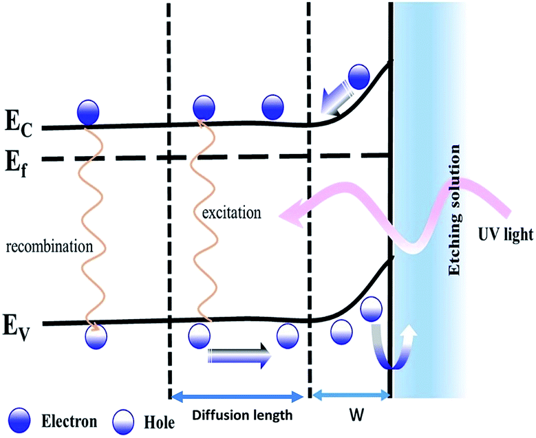 | ||
| Fig. 5 Energy band diagram: between GaN film, electrolyte H2O2:HF:CH3OH. | ||
The PL measurements shown in Fig. 6 were conducted on the samples etched at different times of 90, 180, 240, and 300 min. The emission peaks are predominated by the bound exciton D0x located at 3.425 eV (362 nm) for the as-grown sample, 3.419 eV (362.6 nm) for the sample etched for 90 min, 3.414 eV (363.2 nm) for the sample etched for 180 min, 3.412 eV (363.4 nm) for the sample etched for 240 min, and 3.41 eV (363.7 nm) for the sample etched for 300 min. The PL spectra of the etched samples show a second peak by a donor–acceptor pair (DAP) at around 3.35 eV (370 nm). Therefore, a red-shift is discerned compared with the bulk GaN. This red-shift was attributed to the relaxation of compressive stress in the GaN NWs. Furthermore, the full width at half-maximum (FWHM) of the GaN NWs is broader compared to that of the as-grown sample, and this increase of FWHM could be attributed to the wide size distribution of the nanowires.31,32
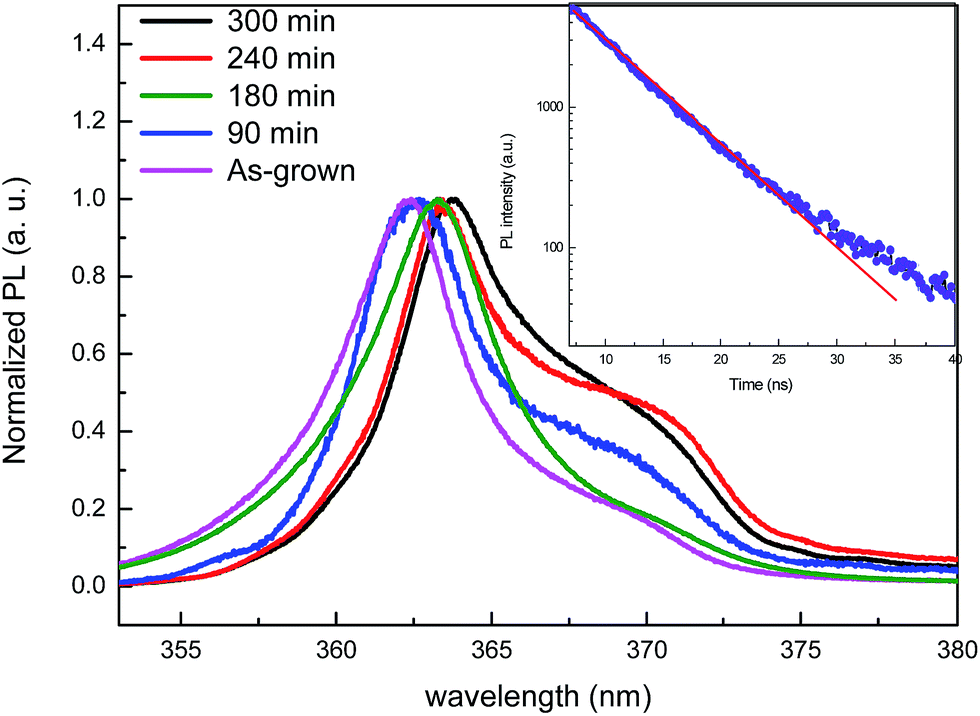 | ||
| Fig. 6 PL spectra of as-grown GaN and GaN NW samples for different etching times: 90, 180, 240 and 300 min. Inset: PL decay of GaN NWs in ethanol from the sample etched for 300 min. | ||
Time-resolved PL measurements on dispersed nanowires in ethanol prepared from the sample etched at 300 min are studied at room temperature, as shown in the inset in Fig. 6. The PL decay was fitted using a single-exponential decay. The lifetime emission was equal to 10 ns. The measured lifetime is longer than the lifetime measured on GaN NWs grown by catalyst-free molecular-beam epitaxy, which is equal to 2 ns at 275 K.33
Temperature dependent photoluminescence spectra of GaN NWs etched at 300 min are shown in Fig. 7. The near-band-edge (NBE) emission is at 3.474 eV at 78 K. As the temperature increases, the peak position shifts to lower energy, and at 300 K, the peak is around 3.41 eV, as shown in Fig. 7(a). Furthermore, the FWHM is increased with temperature. The crystalline property of these GaN NWs prepared by metal-assisted photochemical electroless etching is quite good compared to that of the external catalyst assisted GaN NWs grown using CVD.34 Using the Varshni formula, the energy versus temperature plot can be fitted by the below equation:35
| Eg(T) = Eg(0) − (αT2/(β + T)) |
 | ||
| Fig. 7 (a) Temperature dependent PL spectra of GaN NWs and (b) Varshni fitting for the peak at 3.41 eV with various temperatures. | ||
Raman spectra for the as-grown sample and etched samples are shown in Fig. 8. The Raman spectra reveal that the E1(TO) peak (560.5 cm−1) is visible for the etched samples. The E2 peak positions are located at 570.0 cm−1 for the as-grown sample, 569.4 cm−1 for the etching times of 90 min and 180 min, and 569.0 cm−1 for samples etched for 240 and 300 min. A shift of ΔE2(TO) = 1.0 cm−1 towards the lower wavenumber was measured for the samples at 240 and 300 min etching duration. The shift of E2 to the lower frequency could be explained by the stress relaxation that takes place for the longer etching time. However, a new shoulder appears for the etched samples at 750.5 cm−1. This shoulder peak is attributed to a Froehlich mode due to the anisotropy etching. This observation has also been reported in columnar GaN prepared by illumination assisted anodic etching.38
 | ||
| Fig. 8 Raman spectra of as-grown GaN, GaN NW samples for different etching times of 90 min, 180 min, 240 min, and 300 min. | ||
The residual strain in GaN NWs can be evaluated based on these Raman measurements. The compressive stress (σxx) can be estimated by the expression ΔE2(TO) = Kσxx cm−1 GPa−1, where ΔE2(TO) is the shift in the wavenumber from GaN NWs and the as-grown GaN, which is equal to 1.0 cm−1 for the samples etched for 240 and 300 min, and K is a proportionality factor equal to 4.2 cm−1 GPa−1 for GaN.39,40 The calculated σxx in the GaN NWs equal 0.23 GPa. However, the compressive stress values in the literature for the as-grown and porous GaN prepared by the same method were evaluated to be 0.36 GPa and 0.27 GPa, respectively.8 The compressive stress in the GaN NWs is lower than that in the as-grown sample due to the stress release. Furthermore, the residual strain, εxx, in the GaN NWs can be obtained using the expression σxx = Mf. εxx, where Mf is the biaxial modulus of the GaN substrate equal to 449.6 GPa.41 The residual strain, εxx, in the nanowires is determined to be 2.6 × 10⁻⁴. Hugues et al. shows that the in-plane strain in the GaN NWs prepared by Metal Organic Vapor Phase Epitaxy (MOVPE) is around 1.0 × 10⁻³ and demonstrates that the strain decreases during the first 100–200 nm and is fully relaxed when the nanowire height reaches 300 nm.42 Hence, residual strain measurements have been confirmed, which are one order of magnitude smaller due to the length (few microns) of our nanowires.
Experimental
The unintentionally doped n-type GaN film, used in this study, was grown on a c-axis (0001) sapphire substrate with a resistivity lower than 0.05 Ω cm and was purchased from Xiamen Powerway Advanced Material Co., LT. The thickness of the GaN film was about 30 μm, and the carrier concentration of the film was 3.4 × 1017 cm−3. The GaN samples were cleaned by sonication in acetone, then followed by 2-propanol for 5 min in each solution. This was followed by immersing the sample in HNO3 at 65 °C for 15 min. The samples were then rinsed in DI water and methanol. Two narrow strips of 10 nm thick Pt, separated by a few millimeters, were deposited on the GaN samples using a sputtering system. The samples were etched in the H2O2:HF:CH3OH (2:1:2) solution under UV illumination for different etching times (90, 180, 240, and 300 min). After chemical etching, the samples were removed from the solution and rinsed with DI water. FEI's Magellan 400 FEG scanning electron microscopy (SEM) operating at 5 keV beam energy and high-resolution transmission electron microscopy (HRTEM) were used to analyse the crystal structure, using the FEI's TitanG2 80-300 TEM. The X-ray measurements were performed on Bruker system (D8 Avance). The PL measurements were performed at room and low temperatures using the Jobin Yvon LabRAM HR 800 UV system. The PL decay was measured using a FLS920 fluorescence spectrometer from Edinburgh Instruments with an arc lamp as the excitation source (excitation wavelength at 325 nm). A He Cd laser emitting at 325 nm and a diode-pumped solid-state (DPSS) laser emitting at 532 nm were used as excitation sources for PL and Raman measurements, respectively. The incident laser power for both measurements was set to 20 mW.
Conclusions
In summary, fabrication of GaN NWs with nanoscale dimensions prepared by a metal-assisted photochemical electroless etching technique was investigated with different etching times. With longer etching times, GaN NWs were observed on the surface. The etching mechanism related to the synthesis of GaN NWs and the energy band diagram were presented. The PL measurements reveal that the peak positions of the GaN NW samples were red-shifted due to strain relaxation. The compressive stress and residual strain were determined to be 0.23 GPa and 2.6 × 10⁻⁴, respectively using Raman measurement.Acknowledgements
The authors acknowledge the financial support from the UAE University under Stat-up project No. 31S214.References
- L. Cademartiri and G. A. Ozin, Adv. Mater., 2008, 21, 1013 CrossRef.
- C. M. Lieber, MRS Bull., 2003, 28, 486 CrossRef CAS.
- P. J. Pauzauskie and P. Yang, Mater. Today, 2006, 9, 36 CrossRef CAS.
- F. Glas, Phys. Rev. B: Condens. Matter Mater. Phys., 2006, 74, 121302 CrossRef.
- C. M. Lieber and Z. L. Wang, MRS Bull., 2007, 32, 99 CrossRef CAS.
- Y. Xia, P. Yang, Y. Sun, Y. Wu, B. Mayers, B. Gates, Y. Yin, F. Kim and H. Yan, Adv. Mater., 2003, 15, 353 CrossRef CAS.
- J. C. Johnson, H. Choi, K. P. Knutsen, R. D. Schaller, P. Yang and R. J. Saykally, Nat. Mater., 2002, 1, 106 CrossRef CAS PubMed.
- A. Najar, M. Gerland and M. Jouiad, J. Appl. Phys., 2012, 111, 093513 CrossRef.
- J. Goldberger, R. He, Y. Zhang, S. Lee, H. Yan, H. J. Choi and P. Yang, Nature, 2003, 422, 599 CrossRef CAS PubMed.
- Y. Huang, X. Duan, Y. Cui and C. M. Lieber, Nano Lett., 2002, 2, 101 CrossRef CAS.
- H. Choi, J. Johnson, R. He, S. Lee, F. Kim, P. Pauzauskie, J. Goldberger, R. Saykally and P. J. Yang, J. Phys. Chem. B, 2003, 107, 8721 CrossRef CAS.
- X. Duan and C. M. Lieber, J. Am. Chem. Soc., 2000, 122, 188 CrossRef CAS.
- C. C. Chen, C. C. Yeh, C. H. Chen, M. Y. Yu, H. L. Liu, J. J. Wu, K. H. Chen, L. C. Chen, J. Y. Peng and Y. F. Chen, J. Am. Chem. Soc., 2001, 123, 2791 CrossRef CAS PubMed.
- H. W. Seo, S. Y. Bae, J. Park, H. N. Yang, K. S. Park and S. J. Kim, Chem. Phys., 2002, 116, 9492 CAS.
- Z. Zhong, F. Qian, D. Wang and C. M. Lieber, Nano Lett., 2003, 3, 343 CrossRef CAS.
- D. Tham, C. Y. Nam and J. E. Fischer, Adv. Funct. Mater., 2006, 16, 1197 CrossRef CAS.
- J. L. Weyher, F. D. Tichelaar, D. H. Van Dorp, J. J. Kelly and A. Khachapuridze, J. Cryst. Growth, 2010, 312, 2607 CrossRef CAS.
- J. L. Weyher, J. Smalc-Koziorowsk, M. Bańkowsk, I. Dzięcielewski, Ł. Marona and P. Perlin, J. Cryst. Growth, 2015, 426, 153 CrossRef CAS.
- J. Charrier, A. Najar and P. Pirasteh, Appl. Surf. Sci., 2013, 283, 828–832 CrossRef CAS.
- Y. Qu, H. Zhou and X. Duan, Nanoscale, 2011, 3, 4060–4068 RSC.
- X. Genga, B. K. Duan, D. A. Grismer, L. Zhao and P. W. Bohn, Electrochem. Commun., 2012, 19, 39–42 CrossRef.
- Y. Yang, Y. Ling, G. Wang, X. Lu, Y. Tong and Y. Li, Nanoscale, 2013, 5, 1820 RSC.
- H. Cheng, J. Li, D. Wu, Y. Li, Z. Wang, X. Wang and X. Zheng, J. Nanomater., 2015, 343541 Search PubMed.
- V. Dorogan, I. Tiginyanu, T. Vieru, R. Sturza, H. Hartnagel and C. H. Mutamba, Mold. J. Phys. Sci., 2002, N2, 156 Search PubMed.
- D. Chen, H. Xiao and J. Han, J. Appl. Phys., 2012, 112, 064303 CrossRef.
- B. Senapati, S. K. Samanta, S. Maikap, L. K. Bera and C. K. Maiti, Appl. Phys. Lett., 2000, 77, 1840 CrossRef CAS.
- K. Leung, A. F. Wright and E. B. Stechel, Appl. Phys. Lett., 1999, 74, 2495 CrossRef CAS.
- J. B. Varley, J. B. Weber, A. Janotti and C. G. Van de Walle, Appl. Phys. Lett., 2010, 97, 42106 CrossRef.
- K. Rajeshwar, in Encyclopedia of Electrochemistry, ed. A. J. Bard, M. Stratmann and S. Licht, Wiley-VCH, Germany, 2002, ch. 1, vol. 6 Search PubMed.
- C. Youtsey, G. Bulman and I. Adesida, J. Electron. Mater., 1998, 27, 282 CrossRef CAS.
- A. Mahmood, N. M. Ahmed, Y. Yusof, Y. F. Kwong, C. L. Siang, H. R. Abd and Z. Hassan, Int. J. Electrochem. Sci., 2013, 8, 5801 CAS.
- F. K. Yam, Z. Hassan, L. S. Chuah and Y. P. Ali, Appl. Surf. Sci., 2007, 253, 7429 CrossRef CAS.
- J. B. Schlager, K. A. Bertness, P. T. Blanchard, L. H. Robins, A. Roshko and N. A. Sanford, J. Appl. Phys., 2008, 103, 124309 CrossRef.
- Y. Jinkyoung, J. H. Young, S. J. An and G. C. Yi, Appl. Phys. Lett., 2006, 89, 043124 CrossRef.
- Y. P. Varshni, Physica, 1967, 34, 149 CrossRef CAS.
- V. Bougrov, M. E. Levinshtein, S. L. Rumyantsev and A. Zubrilov, Properties of Advanced Semiconductor Materials: GaN, AIN, InN, BN, SiC, SiGe, John Wiley & Sons, Inc., New York, 2001, pp. 1–30 Search PubMed.
- I. M. Tiginyanu, V. V. Ursaki, V. V. Zalamai, S. Langa, S. Hubbard, D. Pavlidis and H. Föll, Appl. Phys. Lett., 2003, 83, 8 CrossRef.
- I. M. Tiginyanu, A. Sarua, G. Irmer, J. Monecke, S. Hubbard, D. Pavlidis and V. Valiaev, Phys. Rev. B: Condens. Matter Mater. Phys., 2001, 64, 233317 CrossRef.
- C. Kisielowski, J. Kruger, S. Ruvimov, T. Suski, J. W. Ager, E. Jones, Z. Liliental, M. Rubin and E. R. Weber, Phys. Rev. B: Condens. Matter Mater. Phys., 1996, 54, 17745 CrossRef CAS.
- D. G. Zhao, S. J. Xu, M. H. Xie, S. Y. Tong and H. Yang, Appl. Phys. Lett., 2003, 83, 677 CrossRef CAS.
- S. Chichibu, T. Azuhata, T. Sota and S. Nakamura, Appl. Phys. Lett., 1996, 69, 4188 CrossRef CAS.
- M. Hugues, P. A. Shields, F. Sacconi, M. Mexis, M. Auf der Maur, M. Cooke, M. Dineen, A. Di Carlo, D. W. E. Allsopp and J. Zúñiga-Pérez, J. Appl. Phys., 2013, 114, 084307 CrossRef.
| This journal is © The Royal Society of Chemistry 2017 |