
 Open Access Article
 This Open Access Article is licensed under a
 Creative Commons Attribution 3.0 Unported Licence
Electronic to protonic conduction switching in Cu2O nanostructured porous films: the effect of humidity exposure†
Baban P. Dhonge *a,
Suprakas Sinha Ray*ab and
Bonex Mwakikungaa
*a,
Suprakas Sinha Ray*ab and
Bonex Mwakikungaa
aDST-CSIR National Centre for Nanostructured Materials, Council for Scientific and Industrial Research, Pretoria 0001, South Africa. E-mail: bpdonge@gmail.com; rsuprakas@csir.co.za
bApplied Chemistry Department, University of Johannesburg, Doornfontein 2028, Johannesburg, South Africa
First published on 19th April 2017
Abstract
In this paper, we present the first experimental evidence for electronic to protonic conduction switching in p-type semiconducting nanostructured cuprous oxide (Cu2O) porous films when exposed to humidity. We also present a linear response at low relative humidity (RH < 48%). The Cu2O nanostructured porous films were synthesized by spray pyrolysis of a Cu/Cu2O colloidal solution obtained by laser liquid medium ablation of a Cu target in water. The as-prepared and annealed Cu2O films were extensively characterized by scanning electron microscopy, atomic force microscopy, X-ray diffraction analysis, and Raman spectroscopy. The chemiresistor response to RH values from 7.5 to 84% was examined at a temperature of 22 °C and a pressure of 760 mmHg. At RH values below 48%, recombination of the majority charge carrier holes and electrons occurred owing to the dissociation of water molecules near the surface; the RH level was used to quantify the increase in resistance response (RRes). Both devices revealed linear responses to RH (7.5–48%), with a maximum rate of 4.38 ± 0.16%/RH. As the RH increased beyond 48%, proton hopping between the physisorbed water molecules had a larger effect than the electronic conduction, and the response showed the opposite effect. The response exhibited a linear log-normal relationship with higher RH values (56–84%), with a maximum rate of −0.0694 ± 0.002![[thin space (1/6-em)]](https://www.rsc.org/images/entities/char_2009.gif) log(%)/RH. The mechanism for switching the resistive response trend of the Cu2O films is discussed.
log(%)/RH. The mechanism for switching the resistive response trend of the Cu2O films is discussed.
1. Introduction
In the last few decades, the study of morphology-related properties of materials has gained attention owing to the significant influence these properties can have on the performance of a material. Porous materials have been comprehensively researched for use in humidity sensors because of their high surface area and tunable pore sizes.1–4 P-type semiconducting cuprous oxide (Cu2O) with a direct band gap of approximately 2.17 eV has been intensively investigated because of its potential application in various fields, including photovoltaic devices, light-emitting diodes, catalysis, spintronics, photo-electrochemical water splitting, and gas sensing.5–10 The major advantages of Cu2O semiconductors are their nontoxicity and low cost. Electrochemical,11 solvothermal,12 hydrothermal, and calcination techniques13,14 have all been reported to synthesize porous-structured Cu2O. However, spray pyrolysis of colloidal solutions is also known to result in porous thin films and hollow particles.15,16Humidity is a measure of the water content in gaseous atmospheres, and it is measured in terms of absolute and relative humidity (RH). The absolute humidity is defined as the ratio of the water vapor mass in air to the air volume. This metric is classified according to the measurement technique and extent of water vapor as either parts per million (PPM) by weight or volume or the dew/frost point (D/F PT) humidity. PPM and D/F PT sensors measure lower humidity ranges (1 to 10000 ppm) and the full range (ppm to a percentage) of humidity, respectively. RH is defined as the ratio of the amount of water vapor in the air to the maximum (saturated) possible water vapor level at the same temperature and pressure.1–3 RH sensors report the humidity as a percentage (1–100%). Absolute humidity sensors are highly recommended for monitoring trace amounts of moisture, but they are expensive and have poor material stability. In contrast, RH sensors are cost effective, easy to use, and have good material stability. RH sensors measure the changes in physical properties such as the dielectric constant and resistance of the sensing materials, e.g., ceramic oxides, polymers, and semiconducting oxides, as a function of RH. In ceramic oxides, changes in the capacitance and electronic, ionic, and electrolytic conduction depend on superficial water vapor adsorption processes such as chemisorption, physisorption, and capillary condensation. Electron tunneling between OH− or H2O molecules in chemisorbed or initially physisorbed water vapor is responsible for the detection of low humidity levels. At higher humidity levels, physisorbed water vapor, the higher mobility in the multiple layer, and the self-dissociation of water molecules favor the Grotthuss mechanism.17 This causes conduction to occur owing to proton donation between water molecules, known as proton hopping (protonic conduction). Electron tunneling decreases in the presence of protonic conduction in ceramic oxides. In porous ceramic materials, water vapor condenses in the capillary-like pores and forms a liquid-like layer, which leads to electronic conduction.17,18 Polymer-based humidity sensors utilize the same mechanism as ceramic oxides.2,3 In semiconducting oxides, electron tunneling is limited because of the presence of mobile charge carrier electrons (n-type) or holes (p-type).2 The electrons released by the dissociation of water in chemisorption and physisorption processes contribute to conduction at low RH levels, which is known as electronic conduction. For higher humidity levels, both electronic and protonic conduction coexist, which makes the semiconducting oxide a more a useful material for humidity sensors.2,19,20 The coexistence of protonic conduction with electronic conduction for various n-type semiconductors and their composite materials has been reported in the literature.2,4,21–24 However, humidity-sensing studies of p-type semiconducting materials and composites are scarce. Most of the studies available reported on composite semiconducting oxides.25–29
For example, Hsueh et al.25 reported the fabrication of a humidity sensor by growing CuO nanowires (NWs) on the surface of a glass substrate. The results showed that the sensitivity of the sensor increased with increasing RH level, which was due to the p-type nature of the CuO NWs. Li et al.26 reported the humidity-sensing properties of CeO2–NiO nanocomposite materials. Singla et al.27 studied the humidity-sensing behavior of a polyaniline/Mn3O4 composite doped with organic and inorganic acids. The authors concluded that the linear increase in the resistance of the acid-doped composites with increasing RH level was an indication of humidity-sensing behavior. A similar conclusion was reported by Pokhrel and Nagaraja in the case of Cr2O3–MoO3 composites exposed to humid conditions.28 Recently, Wang et al.29 reported the humidity-sensing properties of sea urchin-like CuO modified by reduced graphene oxide (rGO). When they compared the performance in terms of response time and RH value at relatively high humidity conditions, they found that the sensor based on the CuO/rGO composite performed better than the sensors fabricated using pure CuO and rGO. The sensing mechanism was briefly introduced and explained by the Schottky junction theory. However, under low-humidity conditions, the sensor based on the CuO/rGO composite exhibited a smaller response.
This study reports the first experimental evidence for the electronic to protonic switching behavior of a Cu2O nanostructured porous film in the presence of humidity. In recent reports, Bârsan et al.30,31 investigated the conduction mechanism in polycrystalline SnO2 thick sensing films under exposure to CO in the presence of humidity. On the basis of their experimental results, they concluded that for SnO2-based gas sensors, “in normal operating conditions it is possible to switch between a conduction-mechanism controlled by the surface depletion layer to one controlled by the surface accumulation layer”.30 Recently, we reported a p- to n-type transition in the case of onion-like carbon with increasing RH level.32 Our explanation was based on the mechanism proposed for single-walled and multi-walled carbon nanotube-based sensors when they were exposed to humidity.33
For the present work, p-type porous Cu2O porous films were synthesized by spray pyrolysis of a Cu/Cu2O colloidal solution obtained by laser liquid medium ablation of a Cu target in water. The film was subjected to humidity response measurements, which revealed that the resistance increased at low RH levels and decreased at higher RH levels owing to the protonic conduction domination of the electron conduction in the reverse direction. We found that previously proposed mechanisms for semiconductor transitions cannot explain reverse switching from p-type to n-type Cu2O porous nanostructures under exposure to humidity.29–33 Hence, a mechanism for the switching behavior of Cu2O in the presence of humidity is proposed.
2. Experimental methods
A schematic diagram for the laser liquid medium ablation process is shown in Fig. 1(a). In this process, a Nd-YAG pulse laser with a 9 ns pulse width, a 30 Hz frequency, and a 1064 nm wavelength was used to ablate a Cu target under the water. A 12 mm diameter laser beam was reflected using a BK7 (Red Optronics) mirror and focused on a 1 mm diameter spot on the target. The height of the water layer was maintained at 10 mm above the ablating surface. The beaker with the Cu target was continuously rotated using a stepper motor at a speed of 0.5 rpm to ensure uniform ablation and avoid crater formation. A laser fluence of 3.4 J cm−2 was used for the 15 min of the ablation. The inset image in Fig. 1(a) shows the ablated track on the Cu target after two runs of 15 min. The colloidal solution obtained from the 15 min of ablation was characterized using an ultraviolet-visible (UV-vis) spectrophotometer (Perkin Elmer Lambda 750S) and a high-resolution transmission electron microscope (HRTEM, JEOL-JEM 2100, Japan).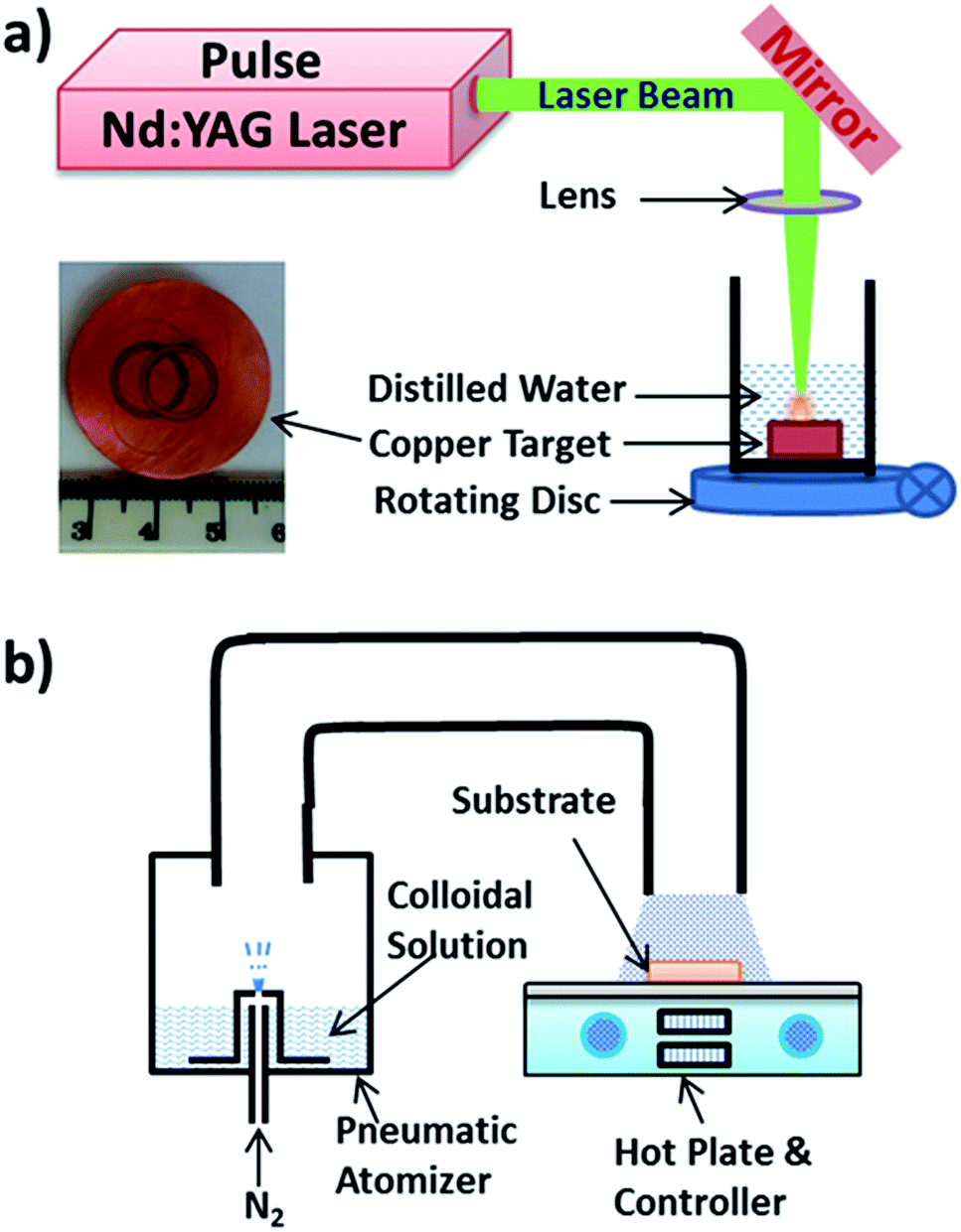 | ||
| Fig. 1 Schematic representation of (a) laser liquid medium ablation and (b) spray pyrolysis technique. | ||
The freshly prepared colloidal solution was used to develop the porous Cu2O film by spray pyrolysis. A schematic representation of the spray pyrolysis process is shown in Fig. 1(b). In this deposition technique, the colloidal solution was pneumatically atomized in the cup using nitrogen at a flow rate of 1500 sccm and an atomization rate of 20 mL min−1. The atomized colloidal aerosols were spread over the substrate, glass, and an alumina sensor strip at 80 °C. An alumina strip (20 × 5 × 1 mm3) pre-printed with a platinum electrode on one side and a resistive heater on the other side was used for the gas-sensing measurements. The surface roughness of the alumina strip was measured to be 17 ± 3 μm. The films were annealed at 200 °C for 3 h. The morphology of the deposits was characterized using field emission scanning electron microscopy (FE-SEM, Zeiss-Auriga Cobra, Germany), the crystal structure was characterized by X-ray diffraction (XRD, PANalytical X'Pert PRO 3040/60, The Netherlands) with Cu Kα radiation (λ = 0.154 nm), and the optical properties were studied by Raman spectroscopy (Horiba Jobin-Yvon HR800, France).
The humidity responses of the as-deposited and annealed films were measured using a gas-sensing system KSGAS6S (KENOSISTEC, Italy). The humidity-sensing measurements were carried out with a 0.5 V direct current (DC) across the electrode. RH levels of 8 to 84% in the sensing chamber (500 mL) were achieved by bubbling water using synthetic air during the response and monitored using a built-in humidity sensor. During the recovery, dry synthetic air was used to fill the chamber. A constant total flow rate of 500 sccm was maintained during the response and recovery. The sensor response to humidity, RRes, was evaluated using the formula RRes = RRH/RA, where RRH and RA are the resistance in the presence and absence of humidity, respectively. The RRH value was measured just before removing the humidity. The response time is defined as the time required for the sensor resistance to reach 90% of the equilibrium value in the presence of humidity and the recovery time is defined as the time required for the sensor to return to 10% above the equilibrium resistance in the absence of humidity. The sensing chamber temperature was monitored during each measurement. The temperature was found to have fluctuated between 20 and 22 °C owing to the application or removal of humidity.
3. Results and discussion
3.1. Cu/Cu2O colloidal solution
Cu and Cu2O have prominent and spectrally distinct features in the visible spectra, which makes it possible to monitor the oxidation reaction through UV-vis spectroscopy. The light green synthesized Cu/Cu2O colloidal solution exhibited an aging effect and was stable for up to 10 days. Afterward, precipitation and a change in color to light brown were observed. The UV-vis spectra of the synthesized and aged colloidal solution, recorded in the 400–800 nm range [Fig. 2(a)], revealed two absorption peaks at 650 and 735 nm. The broad peak centered at 650 nm is recognized as the surface plasmon resonance (SPR) absorption of Cu nanoparticles in the visible spectrum. The SPR observed in the Cu nanoparticles is due to the resonance oscillation of conduction electrons resulting from excitation by electromagnetic radiation.34,35 The shoulder at approximately 735 nm, which is distinct from the plasmon wavelength, is the optical absorption spectra of Cu2O nanoparticles and is characterized by an excitonic peak at a wavelength that corresponds to the band gap.36 The decrease in the intensity of the SPR peak of 21% that occurred after 10 days and disappeared after 20 days indicated further oxidation of Cu and agglomeration of the nanoparticles. A blue shift and broadening of the SPR peak were observed as the sample aged. This phenomenon was attributed to the decrease in the Cu nanocrystal size and changes in the local environment around the Cu nanocrystal. The oxide shell formed at the top of the Cu nanocrystal replaced the interface between the Cu metal and water molecules. In contrast, a red shift and an increase in the intensity of the band-edge excitonic absorption peak at 735 nm corresponding to Cu2O were observed. These changes are attributed to the oxide layer growth trailing that of the Cu nanoparticle. TEM images of a colloidal particle [shown in Fig. 2(b) and (c)] reveal tiny particles approximately 5–15 nm in size and large spherical particles approximately 20–40 nm in size.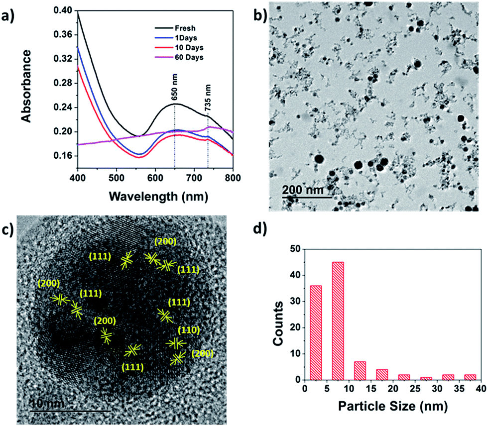 | ||
| Fig. 2 (a) UV-vis spectra of fresh and aged colloidal solution, (b) TEM images of colloidal particles, (c) high-resolution TEM image of a large colloidal particle, and (d) particle-size histogram of colloidal particles. | ||
The particle-size distribution is presented in Fig. 2(d). The large spherical particles grew owing to the agglomeration of tiny particles orientated in various directions, as shown in Fig. 2(c). The spacing between the fringes in the tiny particles correspond to the (111), (110), and (200) planes of Cu2O. The interplanar distance corresponding to Cu was not observed. This may have been due to the oxidation of the Cu nanoparticles in the atmosphere during the TEM sample preparation. The sample was dried at room temperature for 2 h to remove the water, and Cu metal is prone to surface oxidation upon exposure to ambient conditions at room temperature, with Cu2O being the dominant product and copper(II) oxide (CuO) the minor product.37
3.2. Cu2O film
 | ||
| Fig. 3 Surface morphologies of the as-deposited film at 80 °C and the film annealed at 200 °C using [(a) and (c)] SEM and [(b) and (d)] AFM, respectively. The inset images in (a) and (c) show the corresponding cross-sectional images of the films. | ||
The film synthesized at 80 °C reveals a porous structure of well-connected particles. The annealed sample shows increased porosity and particles that are connected via small bridges. The inset images in Fig. 3(a) and (c) show the corresponding cross-sectional images of the films. The film thickness was found to vary between 0.6 to 2.19 μm owing to the porosity and the substrate surface roughness. The surface morphologies of the films acquired using AFM over a 3 × 3 μm2 area are shown in Fig. 3(c) and (d). The spherical particles agglomerated to form porous structures consisting of valleys and hills. The average particle size was measured by considering the cross-sectional diameters of the particles. The particle size and surface roughness decreased from 43 ± 9 nm and 116 nm, respectively, for the as-deposited film to 33 ± 4 nm and 90 nm, respectively, after annealing at 200 °C. The purification of the Cu2O film after annealing thus led to decreases in the particle size and surface smoothness.
 | ||
| Fig. 4 XRD patterns of as-deposited and annealed Cu2O films. | ||
The as-deposited sample at 80 °C reveals the presence of a (111) plane peak of Cu2O (at 2θ = 36.65°) and a (111) plane peak of Cu (at 2θ = 43.37°), with a left shoulder owing to the (200) plane peak of Cu2O. Segregation of these peaks and development of an extra peak at 2θ = 29.72°, corresponding to the (110) plane of Cu2O, were seen after annealing the samples at 200 °C. The particle sizes of various planes were calculated using the Scherrer formula38 and are listed in the Table 1. After annealing the film, the Cu particle shows the growth along the (111) plane and reduces along the (200) plane. On the other hand, Cu2O particle shows the growth along all the major planes of (110), (111), and (200). The particle size observed using AFM was higher than the value calculated from the XRD measurement. Thus, the large particles revealed that the films consisted of Cu, Cu2O, and an amorphous phase.
| Component (plane) | Average particle size (nm) | |
|---|---|---|
| As-deposited at 80 °C | Annealed at 200 °C | |
| Cu (111) | 6.3 | 35.0 |
| Cu (200) | 10.0 | 7.6 |
| Cu2O (110) | — | 13.2 |
| Cu2O (111) | 4.6 | 7.4 |
| Cu2O (200) | — | 5.1 |
The structural properties of both the as-deposited and annealed films were also studied by Raman spectroscopy. CuO had a monoclinic crystal structure, with C2h6 space group symmetry. It had 12 zone-centered optical phonon modes, 4Au + 5Bu + Ag + 2Bg. Among these, three (Au + two Bu) were acoustic modes, six (3Au + 3Bu) were infrared active modes, and three (Ag + 2Bg) were Raman active modes. The Raman active modes—Ag, Bg1, and Bg2—exhibited a quantum confinement effect.39,40 In contrast, Cu2O had a cubic/cupric crystal structure, possessed a C2h6 space group, and had 15 zone-centered optical phonon mode symmetry. One was a Raman active mode, Γ25+, two were infrared active modes, Γ15−(1) and Γ15−(2), three were neither Raman nor infrared active modes (silence mode), Γ25−, Γ12−, and Γ2−, two were second-order overtones, 2Γ12−(2) and 2Γ12−(2), one was a second-order overtone combination (Γ15−(1) + Γ15−(2)), and one was a fourth-order overtone, 4Γ12−.41–43 Fig. 5 shows the Raman spectra of the as-deposited and annealed Cu2O films.
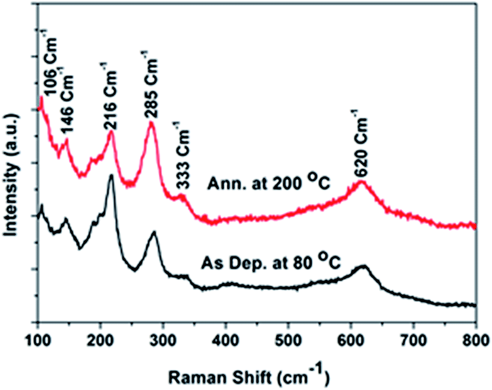 | ||
| Fig. 5 Raman spectra of as-deposited and annealed Cu2O films. | ||
The as-deposited film and the film annealed at 200 °C reveal the presence of Raman peaks corresponding to both oxides, Cu2O and CuO. The silence mode of Γ12− at 106 cm−1 of Cu2O and the acoustic modes of Ag, Bg1, and Bg2 at 285, 333, and 620 cm−1, respectively, of the Raman active mode of CuO, were observed in all the films. The infrared active mode of Γ15−(1) at 148 cm−1 and the second-order overtone of 2Γ12−(2) at 216 cm−1 of Cu2O were observed in the as-deposited and 200 °C annealed films. The presence of the CuO Raman peak further demonstrates the surface oxidation of Cu+ to Cu2+. This could not be detected in the XRD measurement because of the low concentration as compared to the XRD detection level of 5%. The Raman shifts observed from the Raman forbidden modes at 106, 146, and 216 cm−1 reveal a violation of the intrinsic selection rule. This inversion symmetry selection rule violation can be explained by the imperfections or defects in the Cu2O crystal structure that occurred in the presence of metallic Cu and CuO. The presence of Cu was observed in the XRD measurements. Powell et al.43 reported that these Raman forbidden peaks can be enhanced by Cd+ ion irradiation because of the resulting crystal imperfections. Additionally, the resonance excitation wavelength of the Ar laser (514.5 nm) was very near that of the electronic energy level of Cu2O, thus extinguishing the inverse symmetry and leading to a breakdown of the selection rule.43,44 The infrared-allowed and silent modes behaved like active Raman modes, which was predicted by Martin45 because of the one-phonon Raman resonance effect.
 | ||
| Fig. 6 The change in resistance of (a) as-deposited and (b) annealed Cu2O films upon exposure to humidity. | ||
The reduction in the intrinsic resistance to baseline resistance is attributed to the ionization of oxygen, creating an accumulation layer of holes near the surface. Both Cu2O devices were found to be highly conductive for the higher RH levels (≥73%), at which point the resistance decreased on the order of 102 Ω. The decrease in resistance in the presence of humidity is characteristic of n-type metal oxides, in which electrons are the majority charge carriers.2,4 During the recovery, the resistance recovered to a value higher than the baseline resistance within the first few seconds (region C) and then decreased to a value near the baseline resistance (region D).
The response percentage at various RH values was evaluated and the results are presented in Fig. 7. Both Cu2O sensors exhibit a linear increase of response percentage at RH values below 48% [Fig. 7(a)] and a linear log-normal relationship at RH values above 48% [Fig. 7(b)]. At low RH, the rate of increase in response percentages are 4.38 ± 0.16 and 0.56 ± 0.05%/RH for the as-deposited and annealed Cu2O sensors, respectively.
 | ||
| Fig. 7 (a) Change in response percentage for RH values in the 7.5 to 48% range and (b) change in the log-response percentage for RH values in the 56 to 81% range. | ||
The selectivity of the as-deposited Cu2O sensor was approximately eight (4.38/0.56) times higher than that of the annealed Cu2O sensor at low RH and equal to that of the annealed Cu2O sensor at higher RH. The average response and recovery time evaluated for low RH were 151 ± 6 and 145 ± 18 s, respectively. The linear response for the low RH range, 7.5 to 48%, and the comparative response and recovery times will have a significant influence on current humidity sensor research and industrial applications, which are normally limited to RH values greater than 20%27,47–49 where the composite response from electron and the proton conduction is predominant. At RH ≥ 56%, the increase in the log-response percentages are −0.0695 ± 0.006 and −0.0694 ± 0.002log%/RH for the as-deposited and annealed Cu2O sensors, respectively. The response of the as-synthesized film was found to be higher than that of the annealed sample owing to the reduction in the number of surface defects (oxygen vacancies) after annealing. The reduction in the number of surface defects decreased the conductivity of the annealed film. The surface roughness of the annealed film was found to have decreased from 110 to 90 nm in the AFM image; this decreased surface roughness was also responsible for the decreased response. The humidity-sensing measurement was repeated on a second set of samples subjected to the same parameters and annealing conditions; the results are included as ESI data.† Fig. S1(a) and (b) in the ESI† show the changes in the resistance of the second as-deposited film and the second annealed Cu2O film, respectively, upon exposure to humidity and dry air for 5 min each. The baseline resistance (resistance in dry air) of both samples was found to be lower than that of the first set of samples owing to the roughness of the alumina substrate and the porous morphology of the films. The decrease in the base resistance reveals a higher response owing to the increased number of surface defects/oxygen vacancies. However, the RH level for the switching behavior was found to be the same for both sets of samples. In order to reduce the cumulative effect attributed to the short recovery time, the humidity-sensing measurements were carried out with 5 min response and 30 min recovery times. Fig. S2(a) and (b) in the ESI† show the change in resistance of the second set of as-deposited and annealed Cu2O films, respectively, upon exposure to humidity and dry air for 5 and 30 min. The longer recovery time only slightly affected the RH level at the time of switching. The response curve revealed only one spike for 56% RH at the time of removal of humidity and no spike during the exposure to humidity as observed for the higher RH level and in the case of lower recovery time (5 min). Thus, the cumulative effect revealed slight changes in the RH level, corresponding to the switching behavior between 48 and 56% RH.
An abrupt changeover in the response occurred at RH values between 50 and 60%. This abrupt change in linear response with increasing RH has been reported for various materials.21,26,27,50 The RH range within which the response changes varies from material to material, and surface properties such as surface roughness and porosity promote proton hopping. For example, Singla et al.27 reported changes in linear response at 40–60% RH for a polyaniline/Mn3O4 composite doped with organic/inorganic acid. Similarly, Biswas et al.21 reported changes at 55–77% RH for ZnO nanotip arrays, Li et al.26 reported changes at 33–54% RH for a Ce2O–NiO composite, and Chung et al.50 reported changes at 45% RH for anodic aluminum oxide. After the abrupt change, the response continued to increase in the same direction, up to the present results at 50–60% RH. Thus, in the present work, this change is attributed to the protonic conduction contribution to the electronic response. At higher RH values, water adsorption promotes protonic conductivity owing to the polarization effect in the DC resistance measurements. Based on this fact, we propose a mechanism that takes into account the dominant nature of protonic conductivity at higher RH values. The conduction due to electrons cannot be neglected at higher RH values after formation of an electron depletion layer. However, it is not possible to distinguish between the parallel electron and proton conduction that occurs in the applied field direction. The contribution of electronic and protonic conduction shown in Fig. 6 at RH > 48% was allocated to four main regions: (A) electronic and (B) protonic response and (C) protonic and (D) electronic recovery. The response and recovery nature of the curves in regions A, B, C, and D can be explained with the following hypothetical mechanisms.
In general, the oxygen molecule adsorbed on the surface and ionized to form a hole-accumulation layer in p-type oxide semiconductors. In p-type oxide semiconductors, the holes are conducted through the parallel paths of the resistive particle cores (high resistivity) and near-surface regions (low resistivity). With exposure to the target gases, chemoresistive variation occurs at the near-surface regions in p-type oxide semiconductors.51 However, the change in the majority charge carrier from p-type to n-type semiconduction is thought to be very rare in the presence of humidity for both devices.2 The resistance of both devices was on the order of 107 Ω, which is equivalent to that of insulating/ceramic materials at room temperature. The high resistance of both devices suggests a low concentration of holes near the surface of the materials. The electrons associated with Cu impurities also contribute to the resistance because they recombine with the holes. The further increase from the baseline resistance in the presence of humidity is attributed to the recombination of the majority charge carrier holes and electrons released in the water dissociation process. This recombination reduces the number of majority charge carriers near the surface. Thus, both parallel conduction paths for the holes (i.e., particle cores and near-surface regions) become highly resistive, and both devices behave like ceramic humidity-sensing devices for higher RH levels.
The interaction and dissociation of water molecules at the Cu2O surface with increasing RH are illustrated in Fig. 8. The p-type semiconductor oxide surface adsorbs oxygen from its surroundings and subsequently ionizes oxygen by trapping electrons from the valance band, which leads to the formation of a layer of holes near the surface, as shown in Fig. 8(a). The ionization of oxygen at the surface occurs according to the following reactions:52
| O2 (gas) ↔ O2 (adsorbed) | (1) |
| O2 (adsorbed) + e− ↔ O2− | (2) |
| O2− + e− ↔ 2O− | (3) |
| O− + e− ↔ O2− | (4) |
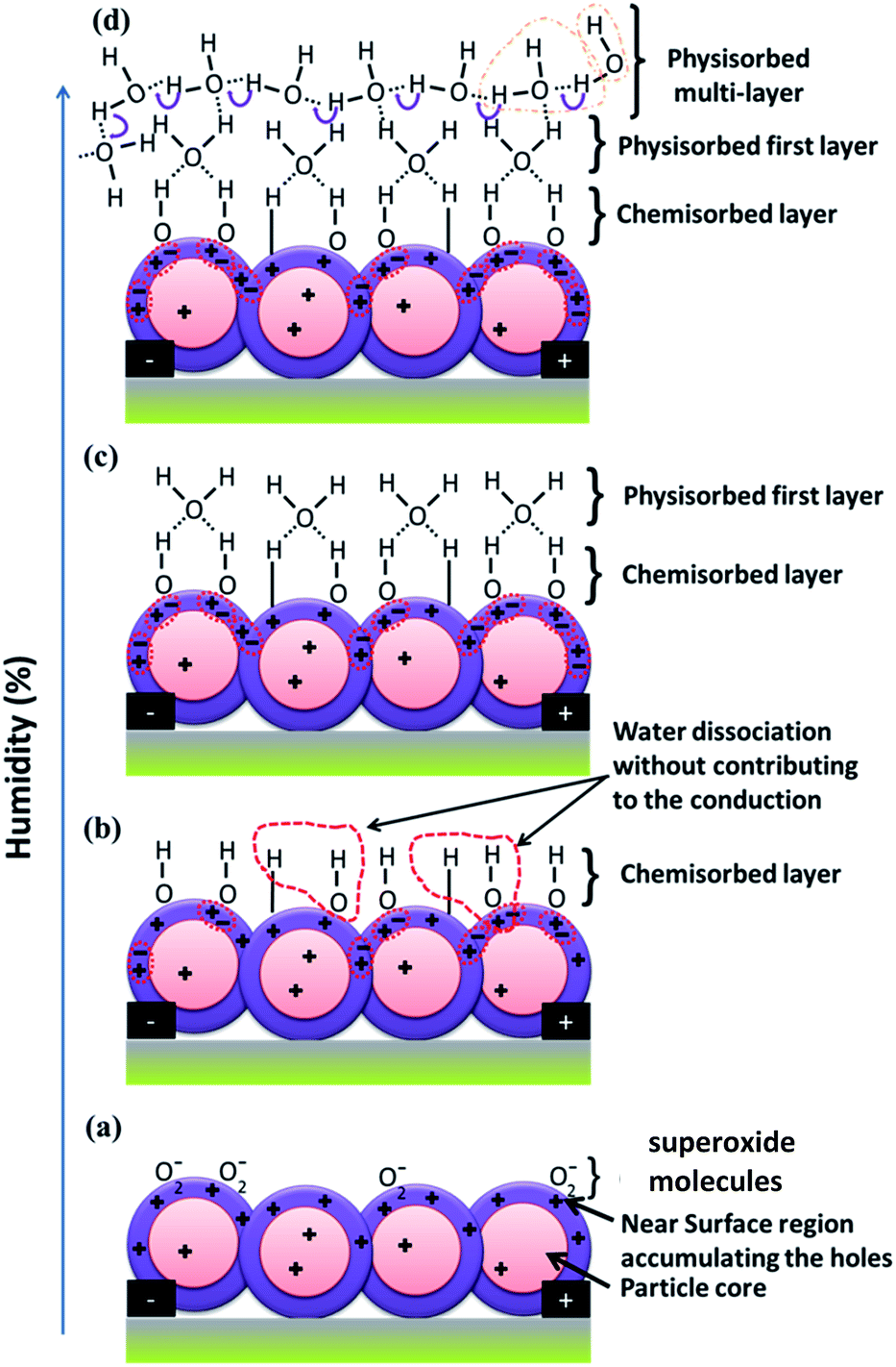 | ||
| Fig. 8 Model for the water molecule interaction and dissociation on the Cu2O surface with increasing humidity percentage: (a) ionization of oxygen leading to the formation of a hole-accumulation layer in the absence of humidity, (b) dissociation of water molecules due to superoxide molecule formation in a chemisorbed OH layer at low RH values, (c) physisorption of water molecules over chemisorbed layer through hydrogen–oxygen partially bonding at RH ≤ 48%, and (d) proton hopping in physisorbed multilayer at RH > 48%. | ||
The ionized oxygen species, O2−, O− and O2−, are known to be dominant below 100 °C, from 100 to 300 °C, and above 300 °C, respectively.52 At room temperature, the superoxide O2− plays an important role in the dissociation of water molecules at room temperature through the following reaction:
 | (5) |
The dissociation of water molecules donates an electron to the conduction. The recombination of electrons released from the superoxide and the majority charge carrier holes results in an increase in the resistance of both devices. Eventually, the water molecules dissociate from the superoxide, leading to the formation of a chemisorbed layer of hydroxide on the surface. In general, the actual coverage of oxygen vacancies on the semiconductor metal oxide surface is less than 1%. Thus, the average distance between oxygen vacant sites is more than 3 nm, i.e., 10 atomic periods of the oxide lattice. However, the water vapor self-dissociates upon interaction with the solid surface heterolytically, the OH− group interacts with an exposed Cu+ cation, and a proton interacts with surface oxygen to yield a second OH− group. This dissociation is not accompanied by charge exchange between the water species and the conduction and/or valance band. Thus, the water self-dissociation and dissociation due to superoxide results in full coverage of the OH− chemisorption layer, as shown in Fig. 8(b). The replacement of superoxide molecules by hydroxide or the dissociation of water molecules depends on the rate at which the water vapor density increases in the chamber and consequently the probability of collisions between the water molecules and the superoxide molecules. A gradual increase in the water vapor density results in a gradual increase in the response (region A) during the electronic response.
During the recovery, the water vapor density in the chamber is reduced to zero. This causes an increase in the partial vapor pressure on the dissociated water molecules, leading to desorption of the water vapor by accepting electrons from the valence band.
The hydroxide molecules continuously replace the superoxide molecules until chemisorbed saturation is reached, at this point, all the superoxide species replaced by hydroxide on the surface and the resistance reaches its maximum value. Thus, at RH levels below 48.2%, most of the holes near the surface recombine with electrons released from the dissociation of water molecules, and conduction occurs through the highly resistive particle core path. The situation becomes identical to that of ceramic humidity sensors for higher RH levels (≥56.37%), in which the electron concentration equals the hole concentration in the near-field region. The recombination of electrons with holes in the hole-accumulation layer leads to the formation of neutral layer, which does not allow further entrainment of the electrons into the layer. Hence, this neutral layer acts as an electron depletion layer. The switching behavior from a hole-accumulation layer to an electron depletion layer and vice versa has been reported for the various gas sensor devices.29–32,53,54 However, the reported mechanisms are not applicable for reverse switching from p-type to n-type Cu2O porous nanostructures under exposure to humidity. In this case, after chemisorbed saturation, the water molecules start to physically absorb on top of the chemisorption layer, as shown in Fig. 8(c). The water molecules are adsorbed through lone oxygen pair interactions with hydrogen from the two neighboring hydroxyl groups. The hydrogen bonds/interactions formed between the water molecules are absent in the first physisorbed layer. Thus, in the first physisorbed layer, the water molecules cannot move freely owing to restrictions from the two hydrogen atoms partially bonded to the oxygen.55 The immobile, chemisorbed, and first physisorbed layers provide for electron tunneling between donor water sites in ceramic materials. However, in p-type semiconductors, in the absence of conduction through the near-surface region, the holes are conducted through the particle core. Thus, electron/hole tunneling in the immobile layer may not be noticeable in the semiconductor.2 The electronic response to higher humidity (>48%) was found to be greater than the response for 48% RH before the protonic response. This may be due to the cumulative effect observed for the low recovery time. That is, with a low recovery time, the base resistance (resistance in dry air) increases after each exposure to humidity. Further exposure to higher RH levels increases the electronic resistance with respect to the new baseline resistance. However, for the higher recovery time of 30 min (see the ESI, Fig. S2†), the base line resistance is nearly constant and the electronic response to higher humidity (>48%) does not exceed the response for 48% RH.
Further condensation of water forms a series of layers on top of the first physisorbed layer to form a multilayer. The order of physisorbed water molecules in the multilayer is due to the fewer numbers (less than two) of localized hydrogen bonds with the water molecules. Water molecules become mobile and finally almost identical to bulk liquid water. In the physisorbed multilayer, the protons (H+) and hydroxide ions (OH−) diffuse owing to surface collisions or self-ionization of water molecules as follows:3
| H2O ↔ H+ + OH− | (6) |
The released hydrogen immediately protonates another water molecule to form a hydronium ion, H3O+, as follows:3
| H2O + H+ ↔ H3O+ | (7) |
Protons from the hydronium ion easily hop across oxygen lone-pairs of water in the presence of an electric field. Oxygen with a lone pair of electrons is responsible for the protonation action in the water molecules. The protons are conducted through the H-bonded networks between water molecules and follow the Grotthuss mechanism.17 The exchange of hydrogen (H+) between hydronium ions (H3O+) and water molecules (H2O) through the oxygen is shown in Fig. 8(d). Proton hopping is a very fast, spontaneous process that occurs in sub-picoseconds. The amount of current drawn as a result of protonic conduction depends on the chain formation between the water molecules in the physisorbed layer.56 Thus, an increase in the condensation rate increases the protonic current. Hence, above 48.2% RH, the Grotthuss mechanism (proton conduction) becomes more dominant than electronic conduction. The water condensation process on top of the first physisorbed layer depends on the water vapor density and time, i.e., low density takes a long time and a higher density takes less time to condense. At RH levels ≥ 48%, the slow rate of condensation leads to a gradual increase in the protonic conduction and hence to a gradual decrease in resistance as a result of protonic conduction in region B. However, during recovery, the physisorbed/condensed water vapor molecules escape rapidly from the surface, leading to the sudden removal of protonic current and consequently a sudden increase in the resistance before it reaches the baseline resistance in region C. The rapid removal of the physisorbed layers may also remove chemisorbed hydroxide without leaving superoxide molecules at the oxygen vacant sites. The absence of superoxide molecule near the surface increases the intrinsic resistance beyond the baseline resistance. With further increases in the RH level, the increase in the condensation of water molecules and hence the increase in the removal of hydroxyl molecules from the surface during recovery leads to an increase in the resistance in region C. Further exposure to dry air during recovery causes the surface to regain superoxide molecules according to eqn (2), and the resistance decreases because of the increase in the number of majority charge carrier holes in region D. However, the simultaneous removal of the chemisorbed layer with the physisorbed layer is energetically not favorable because the chemisorbed OH− molecules include the superoxide, which is tightly bonded to the oxygen vacancies on the surface. The decrease in the binding energy of superoxide after forming OH− molecules and the increase in partial vapor pressure on the dissociated water species should be comparable in order to remove the chemisorbed layer. The H2O molecule adsorption on Cu2O reported by Deng et al.57 reveals OH formation saturated at ∼1% RH, beyond which H2O adsorption without dissociation formed one layer at ∼15% RH, two layers at 35–40% RH, and six layers at ∼90% RH. According to the present conduction mechanism, proton conduction should take place in two layers at 35–40% RH, i.e., in the second physisorbed layer; however, it occurs at RH > 48%, which might be attributed to the surface roughness, causing the formation of a nonuniform second layer below 48% RH.
Switching behavior in the conduction/resistance responses from electron depletion to hole accumulation in n-type and p-type semiconductor oxides upon exposure to the target gases has been reported for various materials.48–52 However, in the present study, the hole-accumulation layer in the p-type semiconductor should change to an electron depletion layer. However, protonic conduction and electronic conduction in the electron depletion layer in the same direction as the applied field are indistinguishable. Also, proton conduction is dominant under DC voltage owing to the polarization effect. Thus, the coexistence of parallel electronic conduction in the depletion layer and proton conduction is conceivable at high RH levels. The protonic conduction resembled the electronic conduction in n-type semiconductors, and the coexistence of both conduction forms led to good humidity sensing as compared to p-type semiconducting materials at high RH.
4. Conclusions
The light green colloidal solution of Cu/Cu2O nanoparticles obtained by LLMA showed aging effects as a result of oxidation and the agglomeration over 10 days. The p-type semiconductor, a Cu2O nanostructure porous film, was obtained by spray pyrolysis of a fresh Cu/Cu2O colloidal solution for the humidity response study. The presence of Cu impurities in the Cu2O film was confirmed using XRD and Raman spectroscopic measurements. The as-deposited and annealed Cu2O films revealed linear relationships at RH < 48% and linear log-normal relationships with RH > 48%. The gradual increase of resistance was constrained by the collision between water molecules and superoxide molecules on the surface, leading to water dissociation processes at lower RH levels (below 48%). With further increases in the RH, the condensation of water molecules on the surface-dissociated molecules promoted protonic conduction. The decrease in the resistive response seen at higher RH levels was because the protonic conduction response to humidity changes was opposite that of the hole conduction response. Thus, the electronic conduction and protonic conduction are distinguishable in p-type semiconductors with fewer majority charge carriers.Acknowledgements
We are grateful for the financial support from the Department of Science and Technology and the Council for Scientific and Industrial Research. The authors sincerely thank the DST-CSIR National Centre for Nanostructured Materials characterization facility team for materials characterization.Notes and references
- Z. M. Rittersma, Sens. Actuators, A, 2002, 96, 196 CrossRef CAS.
- Z. Chen and C. Lu, Sens. Lett., 2005, 3, 274 CrossRef CAS.
- H. Farahani, R. Wagiran and M. Hamidon, Sensors, 2014, 14, 7881 CrossRef PubMed.
- P. M. Faia, E. L. Jesus and C. S. Louro, Sens. Actuators, B, 2014, 203, 340 CrossRef CAS.
- J.-N. Nian, C.-C. Hu and H. Teng, Int. J. Hydrogen Energy, 2008, 33, 2897 CrossRef CAS.
- Z. Q. Yao, S. L. Liu, L. Zhang, B. He, A. Kumar, X. Jiang, W. J. Zhang and G. Shao, Appl. Phys. Lett., 2012, 101, 042114 CrossRef.
- L.-C. Chen, Mater. Sci. Semicond. Process., 2013, 16, 1172 CrossRef CAS.
- R. G. Delatorre, M. L. Munford, R. Zandonay, V. C. Zoldan, A. A. Pasa, W. Schwarzacher, M. S. Meruvia and I. A. Hümmelgen, Appl. Phys. Lett., 2006, 88, 233504 CrossRef.
- Y. Wang, D. Huang, X. Zhu, Y. Ma, H. Geng, Y. Wang, G. Yin, D. He, Z. Yang and N. Hu, Nanoscale Res. Lett., 2014, 9, 1 CrossRef PubMed.
- Y.-K. Lin, Y.-J. Chiang and Y.-J. Hsu, Sens. Actuators, B, 2014, 204, 190 CrossRef CAS.
- Y. Mao, J. He, X. Sun, W. Li, X. Lu, J. Gan, Z. Liu, L. Gong, J. Chen, P. Liu and Y. Tong, Electrochim. Acta, 2012, 62, 1 CrossRef CAS.
- H. Zhang, Q. Zhu, Y. Zhang, Y. Wang, L. Zhao and B. Yu, Adv. Funct. Mater., 2007, 17, 2766 CrossRef CAS.
- G. Zhu, H. Xu, Y. Xiao, Y. Liu, A. Yuan and X. Shen, ACS Appl. Mater. Interfaces, 2012, 4, 744 CAS.
- L.-J. Zhou, Y.-C. Zou, J. Zhao, P.-P. Wang, L.-L. Feng, L.-W. Sun, D.-J. Wan and G.-D. Li, Sens. Actuators, B, 2013, 188, 533 CrossRef CAS.
- Y. C. Kang and S. B. Park, Mater. Lett., 1999, 40, 129 CrossRef CAS.
- S. H. Ju and Y. C. Kang, Mater. Chem. Phys., 2008, 107, 328 CrossRef CAS.
- S. Cukierman, Biochim. Biophys. Acta, Bioenerg., 2006, 1757, 876 CrossRef CAS PubMed.
- B. M. Kulwicki, J. Phys. Chem. Solids, 1984, 45, 1015 CrossRef CAS.
- G. Korotchenkov, V. Brynzari and S. Dmitriev, Sens. Actuators, B, 1999, 54, 197 CrossRef CAS.
- M. Parthibavarman, V. Hariharan and C. Sekar, Mater. Sci. Eng., C, 2011, 31, 840 CrossRef CAS.
- P. Biswas, S. Kundu, P. Banerji and S. Bhunia, Sens. Actuators, B, 2013, 178, 331 CrossRef CAS.
- X. Peng, J. Chu, B. Yang and P. X. Feng, Sens. Actuators, B, 2012, 174, 258 CrossRef CAS.
- Q. Liang, H. Xu, J. Zhao and S. Gao, Sens. Actuators, B, 2012, 165, 76 CrossRef CAS.
- L. Gu, K. Zheng, Y. Zhou, J. Li, X. Mo, G. R. Patzke and G. Chen, Sens. Actuators, B, 2011, 159, 1 CrossRef CAS.
- H. T. Hsueh, T. J. Hsueh, S. J. Chang, F. Y. Hung, T. Y. Tsai, W. Y. Weng, C. L. Hsu and B. T. Dai, Sens. Actuators, B, 2011, 156, 906 CrossRef CAS.
- D. Li, J. Zhang, W. Wei, J. Zhou, S. Wen and S. Ruan, J. Mater. Sci.: Mater. Electron., 2015, 26, 3083 CrossRef CAS.
- M. L. Singla, S. Awasthi and A. Srivastava, Sens. Actuators, B, 2007, 127, 580 CrossRef CAS.
- S. Pokhrel and K. S. Nagaraja, Phys. Status Solidi A, 2002, 194, 140 CrossRef CAS.
- Z. Wang, Y. Xiao, X. Cui, P. Cheng, B. Wang, Y. Gao, X. Li, T. Yang, T. Zhang and G. Lu, ACS Appl. Mater. Interfaces, 2014, 6, 3888 CAS.
- N. Barsan, J. Rebholz and U. Weimar, Sens. Actuators, A, 2015, 207, 455 CrossRef CAS.
- N. Bârsan, M. Hübner and U. Weimar, Sens. Actuators, B, 2011, 157, 510 CrossRef.
- B. P. Dhonge, D. E. Motaung, C.-P. Liu, Y.-C. Li and B. W. Mwakikunga, Sens. Actuators, B, 2015, 215, 30 CrossRef CAS.
- A. Zahab, L. Spina, P. Poncharal and C. Marlière, Phys. Rev. B: Condens. Matter Mater. Phys., 2000, 62, 10000 CrossRef CAS.
- S. Eustis and M. A. El-Sayed, Chem. Soc. Rev., 2006, 35, 209 RSC.
- I. Pastoriza-Santos, A. Sánchez-Iglesias, B. Rodríguez-González and L. M. Liz-Marzán, Small, 2009, 5, 440 CrossRef CAS PubMed.
- K. P. Rice, E. J. Walker, M. P. Stoykovich and A. E. Saunders, J. Phys. Chem. C, 2011, 115, 1793 CAS.
- J. H. Kim, S. H. Ehrman and T. A. Germer, Appl. Phys. Lett., 2004, 84, 1278 CrossRef CAS.
- A. L. Patterson, Phys. Rev., 1939, 56, 978 CrossRef CAS.
- H. F. Goldstein, D.-S. Kim, P. Y. Yu, L. C. Bourne, J. P. Chaminade and L. Nganga, Phys. Rev. B: Condens. Matter Mater. Phys., 1990, 41, 7192 CrossRef CAS.
- M. H. Chou, S. B. Liu, C. Y. Huang, S. Y. Wu and C. L. Cheng, Appl. Surf. Sci., 2008, 254, 7539 CrossRef CAS.
- P. Y. Yu and Y. R. Shen, Phys. Rev. B: Solid State, 1975, 12, 1377 CrossRef CAS.
- K. Reimann and K. Syassen, Phys. Rev. B: Condens. Matter Mater. Phys., 1989, 39, 11113 CrossRef.
- D. Powell, A. Compaan, J. R. Macdonald and R. A. Forman, Phys. Rev. B: Solid State, 1975, 12, 20 CrossRef CAS.
- P. F. Williams and S. P. S. Porto, Phys. Rev. B: Solid State, 1973, 8, 1782 CrossRef CAS.
- R. M. Martin, Phys. Rev. B: Solid State, 1971, 4, 3676 CrossRef.
- S. Hong, D. Xiao Long, I. Hwang, J.-S. Kim, Y. Chang Park, S.-O. Kang and B. Ho Park, Appl. Phys. Lett., 2011, 99, 052105 CrossRef.
- Q. Kuang, C. Lao, Z. L. Wang, Z. Xie and L. Zheng, J. Am. Chem. Soc., 2007, 129, 6070 CrossRef CAS PubMed.
- S. Borini, R. White, D. Wei, M. Astley, S. Haque, E. Spigone, N. Harris, J. Kivioja and T. Ryhänen, ACS Nano, 2013, 7, 11166 CrossRef CAS PubMed.
- G.-Y. Li, J. Ma, G. Peng, W. Chen, Z.-Y. Chu, Y.-H. Li, T.-J. Hu and X.-D. Li, ACS Appl. Mater. Interfaces, 2014, 6, 22673 CAS.
- C. K. Chung, O. K. Khor, C. J. Syu and S. W. Chen, Sens. Actuators, B, 2015, 210, 69 CrossRef CAS.
- H.-J. Kim and J.-H. Lee, Sens. Actuators, B, 2014, 192, 607 CrossRef CAS.
- K. Wetchakun, T. Samerjai, N. Tamaekong, C. Liewhiran, C. Siriwong, V. Kruefu, A. Wisitsoraat, A. Tuantranont and S. Phanichphant, Sens. Actuators, B, 2011, 160, 580 CrossRef CAS.
- A. A. Vasiliev and M. A. Polykarpov, Sens. Actuators, B, 1992, 7, 626 CrossRef.
- Y.-C. Lee, Y.-L. Chueh, C.-H. Hsieh, M.-T. Chang, L.-J. Chou, Z. L. Wang, Y.-W. Lan, C.-D. Chen, H. Kurata and S. Isoda, Small, 2007, 3, 1356 CrossRef CAS PubMed.
- E. McCafferty and A. C. Zettlemoyer, Discuss. Faraday Soc., 1971, 52, 239 RSC.
- R. Pomès and B. Roux, Biophys. J., 1996, 71, 19 CrossRef.
- X. Deng, T. Herranz, C. Weis, H. Bluhm and M. Salmeron, J. Phys. Chem. C, 2008, 112, 9668 CAS.
Footnote |
| † Electronic supplementary information (ESI) available: Additional results related to the change in resistance of as-deposited and annealed CuO2 films on expose to humidity and dry air at various time intervals. See DOI: 10.1039/c7ra00383h |
| This journal is © The Royal Society of Chemistry 2017 |