
 Open Access Article
 This Open Access Article is licensed under a Creative Commons Attribution-Non Commercial 3.0 Unported Licence
Modulation of silicene properties by AsSb with van der Waals interaction
Cui Jin,
Ying Dai *,
Wei Wei,
Qilong Sun,
Xinru Li and
Baibiao Huang
*,
Wei Wei,
Qilong Sun,
Xinru Li and
Baibiao Huang
School of Physics, State Key Laboratory of Crystal Materials, Shandong University, Jinan 250100, China. E-mail: daiy60@sina.com
First published on 17th January 2017
Abstract
Opening a sizable and tunable band gap in silicene without degrading the carrier mobility is quite desirable for high-speed switching devices. In the present work, the structural and electronic properties of two-dimensional silicene modulated by AsSb with van der Waals (vdW) interaction are investigated by density functional theory with vdW corrections. Notably, there is almost no lattice mismatch introduced in silicene/AsSb heterointerface, which is quite beneficial in comparison with silicene on other substrates. A sizable band gap (213–563 meV) appears in silicene owing to the breaking of the inversion symmetry due to the interface effects, which reveals a potential in applications in such as field effect transistors (FETs) at room temperature. In addition, the nearly linear band dispersion of silicene, guaranteeing the high carrier mobility, can be preserved in silicene/AsSb heterostructures considered in this work. Furthermore, the band gap can be effectively tuned by changing the interlayer distance between silicene and AsSb and, interestingly, an indirect–direct band gap transition occurs. Our results provide a possible direction for experimental fabrication and the applications of silicene-related materials.
I. Introduction
Silicene is currently a compelling topic in the research community of two-dimensional (2D) materials due to its unique properties and potential applications. Because of the sp2–sp3 hybridization,1,2 freestanding silicene represents a buckled 2D hexagonal lattice. An analogue of graphene, the band structure of silicene shows a character of zero-gap with the Dirac cone located at the K point of the hexagonal Brillouin zone.3,4 In light of the nearly massless Dirac fermion character,5,6 the extremely high carrier mobility with intrinsic value of 105 cm2 V−1 s−1 is expected in silicene from theoretical estimations.7 Thus, the intriguing electronic properties make silicene a promising material for the high-performance field effect transistors (FETs). Recently, silicene-based FETs have been fabricated, which shows the expected ambipolar Dirac charge transport and opens a new way towards silicene-based nanoelectronics.8 Apparently, pristine silicene cannot directly be used in FETs due to the zero-band-gap. Therefore, opening a sizable and tunable band gap in silicene without degrading its carrier mobility is highly desirable for electronic applications.9,10In view of whether the integrity of honeycomb structure is kept, there are usually several approaches to open a band gap in silicene. On one hand, shaping silicene into nanoribbons,11,12 ad-atoms absorption13–16 and introducing defects in silicene17,18 can give rise to a band gap in silicene. However, it inevitably damages the structure of silicene, significantly reducing the carrier mobility. On the other hand, breaking the inversion symmetry of silicene can also open a band gap, which is usually realized by adopting external electric field19–22 or noncovalent silicene–substrate interaction.23–26
In fact, silicene is always realized on metallic substrates,27–37 which is undesired in FETs because the electronic properties of silicene would be greatly damaged by the metal substrates. The π bands of silicene strongly hybridize with substrate destroying the Dirac cone,38,39 and then the carrier mobility should be greatly reduced.36 With an appropriate non-metallic substrate, such as the GaS,40,41 SiC(0001),42,43 Si,44 diamond,23 ZnS(0001),45 CaF2(111),46 MgBr2(0001),47 MoS2 48 and Sc2CF2,49 a redistribution of charge exists within the interface formed between silicene and the non-metallic substrate.50 By building an interlayer potential difference, the different Coulomb fields felt by A and B sublattices in silicene result in a charge redistribution and the band gap opening.38,51 For example, affected by SiH/π interactions, the equivalence of two sublattices are broken and the silicene/silicane (the fully hydrogenated silicene with hydrogen atoms bonded alternatively up and down to a silicon atom) bilayer has a band gap of 120 meV.43,44 In addition, it is also predicted that the Dirac cone of silicene will maintain in the band gap of Sc2CF2 substrate with a sizable gap (36–48 meV).49
However, there are still some drawbacks as these semiconducting materials are used as substrates for silicene. Firstly, the matched structure usually forms when the mismatch between lattice constants is small.52 So a large lattice mismatch would be a big obstacle in experiments, such as silicene on GaS40,41 and diamond.23 Secondly, similar to metallic substrates, the linear energy band dispersion characteristic will be destroyed, such as silicene/ZnS(0001) interface.45 Then the carrier mobility of silicene should be greatly reduced, which is also a critical factor for the high-performance FETs applications. Finally, and most importantly, silicene with a band gap about 0.1 eV is quite desirable at room temperature for applications in nanoelectronics. However, the band gap of silicene is very small on some substrates, such as the hydrogenated SiC(0001)42,43 and MgBr2(0001).47 Therefore, a new promising material as the substrate for silicene is still highly demanded.
Since the discovery of graphene in 2004, various new 2D materials possessing novel properties are theoretically predicted or experimentally confirmed, such as monolayer (ML) hexagonal boron nitride,53 MoS2,54,55 and WS2.56 Very recently, the As and AsSb monolayers have been predicted theoretically.57–61 It is reported that As and AsSb monolayers are indirect semiconductors with a tunable band gap via applying strain or tailoring into nanoribbons. In addition, AsSb monolayer presents a weak Rashba effect due to the non-symmetric structure and spin orbit coupling. It should be noted that the lattice parameters of AsSb monolayer is predicted to about 3.86 Å, which is the same to silicene, leading to a negligible lattice mismatch.60,61 Thus, it will greatly benefit the experimental fabrication of the silicene/AsSb van der Waals (vdW) heterostructures. It is of importance that, in a vdW heterostructure, the band structure properties of silicene can be preserved under certain conditions due to the weak interactions.
In this work, we theoretically explore the effect of AsSb on tuning the structural and electronic properties of silicene with vdW interaction based on the density functional theory (DFT). Our results provide a detailed understanding for the interfacial properties of silicene/AsSb heterostructures. We predict that a sizable band gap is obtained owing to the breaking of the inversion symmetry of silicene caused by the intrinsic interface dipole. In addition, the nearly linear band dispersion of silicene, guaranteeing the high carrier mobility, can be preserved in the composite. Furthermore, the electronic properties are very sensitive to the interlayer spacing. Our results offer a possibility for the experimental fabrication and applications of silicene-related materials.
II. Computational methods
All the calculations are performed by means of first-principles DFT,62,63 as implemented in Vienna Ab-initio Simulation Package (VASP),64,65 within the framework of the projector augmented wave (PAW) method.66 The generalized gradient approximation (GGA) with the Perdew–Burke–Ernzerhof (PBE)67,68 functional is utilized to describe the exchange correlation interactions. Due to the existence of weak interactions between silicene and AsSb monolayers, the PBE functional with vdW corrections (PBE-D2)65 is chosen for a better description of the long range vdW interactions, which revealed accurate results for the silicene-related heterostructures under certain conditions.42,49 The interlayer distance and band gap were calculated with the revB86b-DF2 functional to verify our computations.69 In addition, the hybrid functional method (HSE) was also employed for exploring the electronic properties. Generally, HSE06 method including 25% Hartree–Fock (HF) exchange can accurately present the experimental band gap for many semiconductors.70 A cutoff energy of 470 eV is used for the plane wave expansion of the wave function, and a 15 × 15 × 1 k-mesh was used for Brillouin zone integrations. By using the conjugate gradient method, the structure relaxations are carried out until the residual forces on the atoms are less than 0.02 eV Å−1. The convergence criterion of self-consistent calculations for ionic relaxations is set to 10−4 eV between two consecutive steps. The heterostructures are modeled by stacking a 1 × 1 lateral periodicity of silicene on a 1 × 1 lateral periodicity of AsSb monolayer. A vacuum layer of 15 Å is used in the direction normal to the interface to avoid unphysical interactions between periodic images. In addition, ab initio molecular dynamics (AIMD) simulations are carried out to examine the thermal stability by using a 3 × 3 silicene supercell at 300 K within each time step of 1 fs.III. Results and discussion
As a starting point, the structural and electronic properties of the free-standing silicene and AsSb monolayer are studied. The top and side views of silicene and AsSb are shown in Fig. 1. Through structural optimization, we obtained the stable low-buckled geometry of silicene with the lattice constant a1 = 3.86 Å and the Si–Si distance d1 = 2.28 Å, while the lattice constant for AsSb is a2 = 3.86 Å and the As–Sb distance is calculated to be d2 = 2.69 Å. We also obtained the buckling height along the z direction, which is h1 = 0.44 Å for silicene and h2 = 1.51 Å for AsSb. The relaxed structural parameters of silicene and AsSb are summarized in Table 1, which is in good agreement with other reports.43,60 Remarkably, almost no lattice mismatch is introduced in silicene/AsSb heterostructures. This is quite beneficial in comparison with the lattice mismatch for silicene on other semiconductors, such as h-BN (2.08%),42 Sc2CF2 (0.68%)49 and MoS2 monolayer (2.42%).48 The lattice mismatch is low enough to avoid experimental problems with a controlled growth, which offers the possibility to form the coherent interfaces. In addition, we calculated the lattice constant of AsSb with SOC (spin–orbit coupling) considered in order to check the effects of spin–orbit interaction. In this case, the lattice constant of AsSb is calculated to be 3.86 Å, which is identical to the result at PBE level of theory, confirming the negligible effects of SOC on the lattice constant of AsSb. | ||
| Fig. 1 Top and side views of the relaxed atomic structures of silicene (a and b) and AsSb monolayer (d and e). Corresponding band structure with the HSE06 method of free-standing silicene (c) and isolated AsSb monolayer (f). The blue, green, and brown balls represent Si, As, and Sb atoms, respectively. The unit cell is represented by the solid lines. The valence band maximum (VBM) of the heterostructures is set to zero. | ||
| Monolayer | a (Å) | d (Å) | h (Å) | Eg (eV) | Eg-hse (eV) |
|---|---|---|---|---|---|
| Silicene | 3.86 | 2.28 | 0.44 | 0 | 0 |
| AsSb | 3.86 | 2.69 | 1.51 | 1.48 | 2.02 |
In order to investigate the configuration dependency of the energetics and electronic structures of silicene/AsSb hybrids, six representative arrangements are considered: (i) in configuration I, all the higher buckled Si (A) atoms of silicene are placed directly above the As atoms of AsSb, while the remaining lower buckled Si (B) atoms are located directly above the Sb atoms of AsSb, as shown in Fig. 2(a) and (g). (ii) In configuration II, all the lower buckled Si (B) atoms are right above the As atoms, while the Sb sublattice are located below the hollow sites of silicene, as shown in Fig. 2(b) and (h). (iii) In configuration III, all the higher buckled Si (A) atoms are right above Sb atoms, while the As sublattice are below the hollow sites of silicene, as shown in Fig. 2(c) and (i). (iv) In configuration IV, all the higher buckled Si (A) atoms of silicene are placed directly above the Sb atoms of AsSb, while the remaining lower buckled Si (B) atoms are located directly above the As atoms of AsSb, as shown in Fig. 2(d) and (j). (v) In configuration V, all the lower buckled Si (B) atoms are right above the Sb atoms, while the As sublattice are located below the hollow sites of silicene, as shown in Fig. 2(e) and (k). (vi) In configuration VI, all the higher buckled Si (A) atoms are right above As atoms, while the Sb sublattice are below the hollow sites of silicene, as shown in Fig. 2(f) and (l). We have also examined the other possible geometries which are not highly symmetric, as shown in Fig. 3. However, after geometry relaxation, these configurations will converge to the configurations depicted in Fig. 2 to minimize the total energy. In addition, we confirmed that silicene on multilayer AsSb show almost the same electronic structures, which is due to the weak vdW interlayer interactions and only the first AsSb layer affects the properties of silicene.
 | ||
| Fig. 2 Top and side views of the relaxed atomic structures of the six arrangements for silicene/AsSb heterointerface: configuration I (a and g), configuration II (b and h), configuration III (c and i), configuration IV (d and j), configuration V (e and k) and configuration VI (f and l). The blue, green, and brown balls represent Si, As, and Sb atoms, respectively. The unit cell is represented by the solid lines. | ||
 | ||
| Fig. 3 Top views of silicene/AsSb heterostructures with possible geometries. The blue, green, and brown balls represent Si, As, and Sb atoms, respectively. The unit cell is represented by the solid lines. | ||
The optimized interlayer spacing between silicene and AsSb is summarized in Table 2. We found that the interlayer distance calculated with PBE-D2 is quite similar with the results of revB86b-DF2 functional, indicating that the PBE-D2 method can work well for this silicene/AsSb heterostructures system and, however, it does not necessarily indicate the general reliability of PBE-D2 for these kind of systems. Irrespective of the stacking arrangements, there are no obvious changes in the surface structures of silicene compared with the isolated monolayer. Apparently, the buckling height of silicene amounts to 0.50–0.63 Å, which is mildly larger than that of free-standing one (0.44 Å). And it is much smaller than that of silicene on Ag(111) (∼0.9 Å),71 indicating a weak structural distortion induced by AsSb.
| Configurations | Eb (meV) | d0 (Å) | d1 (Å) | Eg (meV) | Eg1 (meV) | Eg-HSE (meV) |
|---|---|---|---|---|---|---|
| I | −837 | 2.96 | 3.05 | 117 | 101 | 213 |
| II | −929 | 2.54 | 2.63 | 214 | 255 | 340 |
| III | −941 | 2.63 | 2.62 | 318 | 378 | 563 |
To further demonstrate the stability of the silicene/AsSb heterostructures, we also carried out AIMD simulations at room temperature (T = 300 K) with a time step of 1 fs. After running 3000 steps, no bond breaking and structure reconstruction are found, which suggests that these configurations are stable enough. Take configuration III as an example, the fluctuation of free energy with time at the temperature of 300 K is shown in Fig. 4, with the fluctuant energy being about 0.6 eV, which further proves that these configurations are thermodynamically stable at room temperature.
 | ||
| Fig. 4 Variation of the total energy within 3 ps during AIMD simulation at 300 K for configuration III. | ||
As shown in Fig. 1(c), the band structure of silicene features a Dirac-type electron dispersion in the vicinity of its hexagonal Brillouin zone corners. Meanwhile, AsSb monolayer exhibits a semiconducting character with an indirect band gap (1.48 eV at PBE level of theory and 2.02 eV at HSE06 level of theory), which is consonant with previous computational results,60 see Fig. 1(f). To get a better understanding on the properties of silicene/AsSb heterostructures, we calculated the electronic band structures. Fig. 5 displays the band structures for the silicene/AsSb heterostructures with different stacking patterns. The energy states near the Fermi level are mainly dominated by the π and π* bands of silicene, suggesting the electronic transport behaviors of the hybrid structures are mainly determined by the 3pz states of silicene. In comparison with Fig. 5(a)–(c), band structures shown in Fig. 5(d)–(f) present quite similar features with respect to the band dispersion relationship and band gap. As a result, we will focus on the heterostructures with silicene stacked on the As-side of AsSb in following discussions about the electronic properties.
 | ||
| Fig. 5 Band structures of the six silicene/AsSb heterostructures at HSE06 level of theory: configuration I (a), configuration II (b), configuration III (c), configuration IV (d), configuration V (e) and configuration VI (f). The valence band maximum (VBM) of the heterostructures is set to zero. | ||
In order to quantitatively characterize the interface binding properties, the binding energy (Eb) between silicene and AsSb is calculated as
| Eb = Etotal − Esilicene − EAsSb |
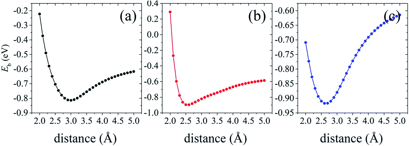 | ||
| Fig. 6 Binding energy Eb variation as a function of the distance between the lowest Si atoms in silicene and the topmost As atoms in AsSb for the three silicene/AsSb arrangements: configuration I (a), configuration II (b) and configuration III (c). | ||
Silicene on AsSb monolayer loses its linear band dispersion with massless electrons, but rather semiconducting properties with π and π* bands separating from each other at the K point. This indicates that the on–off current ratio would be greatly improved in the silicene/AsSb heterointerface logical devices. As shown in Table 2, considerable band gap is opened in silicene/AsSb heterostructures (117 meV, 214 meV and 318 meV at PBE level of theory for configuration I, configuration II and configuration III, respectively), which is more pronounced than the room temperature thermal scale (26 meV), indicating the stability above room temperature. Notably, band gap of silicene/AsSb heterostructures is quite larger in comparison with that of silicene on other semiconductors. For comparison, we calculated the band gap with revB86b-DF2 functional, which reveals similar results, as shown in Table 2. In the case of configuration III, for example, the largest difference in band gap of 60 meV is obtained among all the configurations considered. It can be verified that the PBE-D2 method can provide reliable results for the electrical properties of silicene/AsSb vdW heterostructures. Again, however, it does not guarantee the general reliability of PBE-D2 method to other systems. To further explore the band gap more accurately, band gaps calculated from the HSE06 method are also considered. As shown in Table 2, much larger band gaps are demonstrated (213 meV, 340 meV and 563 meV at HSE06 level of theory for configuration I, configuration II and configuration III, respectively), indicating that the silicene/AsSb heterostructures are quite good candidate materials for the application of silicene-related electronic device.
Different configurations exhibit different electronic features near the Fermi level, as plotted in Fig. 5(a)–(c). We also find that configuration I presents a direct band gap with the conduction band minimum (CBM) and valence band maximum (VBM) located at the K point, while configuration II and configuration III turn out to be indirect band gap. It is noted that configuration III is the most stable stacking pattern, which would be more easily obtained in experiments. The band gap value of 563 meV is much larger than configurations I and II, which would more easily overcome one of the main obstacles, the lack of intrinsic band gap, to apply silicene as an electronic device.8–10 In addition to the larger band gap, band structure of configuration III also suggests relatively high electron mobility in comparison to that of configuration I. Accordingly, configuration III with the sizable band gap and relatively high electron mobility indicates the potential for practical applications in silicene-related electronic devices.
Careful examination of the band structure at the K-point for configuration I, as shown in Fig. 5(a), indicates that the nearly linear band dispersion of silicene can be preserved in configuration I. The typical conical structure of silicene π bands in the vicinity of Fermi level is almost comparable to the free-standing silicene. The Dirac cone is almost preserved but slightly deformed near the K point due to a gap opening of 213 meV, indicating an extremely high carrier mobility with small electron effective mass. It is mainly due to the relative weak interface interaction and the associated changes in silicene lattice. Note that, when silicene deposited on metallic substrates or non-metallic substrates, the linear band dispersion characteristics can be destroyed. In comparison to configurations II and III, configuration I is not the most stable one. However, some research group has reported the realization of vertical heterostructures of transition-metal dichalcogenide (TMD) layers using the chemical vapor deposition (CVD),76–79 where the morphology can also be adjusted through the local substrate environment. This approach will lead to better control over the stacking alignment and the interface quality in vertical heterostructures. As a consequence, configuration I can also probably be obtained experimentally under certain conditions. Since the presence of a desirable band gap without degrading the electronic properties of silicene is highly expected, AsSb should be a suitable choice as the substrate for silicene-related electronic devices.
We further investigate the variation of band gap feature as the interlayer spacing changes. The complicated change trends of band gap can be observed in Fig. 7. In the shadow free region with the increasing of interlayer distance, the interaction between silicene and AsSb becomes weak. Then there is a clear monotonically reduction trend of the band gap, even to zero, bringing about a semiconductor–metal transition. On the contrary, if the interlayer distance decreases, the energy gap will increase significantly due to the strong hybridization between Si-3p and As-4p orbitals. In the shadow region with the decreasing of interlayer distance, the band gap also gradually reduced to zero. It is noticeable that, silicene/AsSb heterostructures turn out to be metallic when the distance is around 2.0 Å. Simultaneously, there also exists an indirect–direct gap transition (shadow region represents the indirect gap and the shadow free region represents direct gap) by varying the interlayer spacing of these configurations. It can be understood that the stronger interlayer interactions accordingly lead to an indirect band gap rather than the direct. Therefore, it is an effective way to notably modulate the band gap of silicene and a viable route for the design of silicene-based FETs.
 | ||
| Fig. 7 Band gap variation as a function of the distance between the lowest Si atoms in silicene and the topmost As atoms in AsSb for the three silicene/AsSb heterostructures: configuration I (a), configuration II (b) and configuration III (c). | ||
Charge density difference (CDD) is useful in the analysis of the properties of heterostructures. To visualize the electron redistribution upon the formation of silicene/AsSb heterointerfaces, and gain more insights into the opened band gap, we defined the CDD as
| Δρ = ρtotal − ρsilicene − ρAsSb |
 | ||
| Fig. 8 Charge density difference (CDD) of silicene on AsSb monolayer for the three silicene/AsSb heterostructures: configuration I (a), configuration II (b) and configuration III (c). Yellow (cyan) color represents charge accumulation (depletion), and the isosurface value is 0.0005 e Å−3. The blue, green, and brown balls represent Si, As, and Sb atoms, respectively. The unit cell is represented by the solid lines. | ||
As shown in Fig. 8, the electron configurations for different stacking patterns are different, which can explain the electronic structure variation depending on the configuration. Compared to configurations II and III, the CDD for configuration I indicates relatively small charge redistribution within the interface region, indicating relatively small interface interaction. In addition, interlayer distance also reflects the interlayer interaction. In this situation, the on-site energy of silicon atoms in the two sublattices of silicene can be changed to different extent and therefore the electronic structures show difference with respect to the interlayer distance. In configuration I, for example, the small interlayer interaction well preserves the nearly linear band dispersion of silicene, guaranteeing the high carrier mobility.
IV. Conclusions
In conclusion, the manipulation of structural and electronic properties of silicene by AsSb with vdW interaction are comprehensively studied by means of first-principles calculations. A series of representative stacking patterns of silicene on AsSb monolayer are considered. Our results indicate that these configurations would be stable well above room temperature, and there exists a charge redistribution near the interface due to the interaction of two components. Notably, a sizable band gap in the range of 213–563 meV is opened in silicene/AsSb due to the inversion symmetry broken by intrinsic interface dipole. Moreover, the calculated band gaps for three stacking patterns are considerably larger than kBT (26 meV) at room temperature, which may overcome one of the main obstacles, the lack of intrinsic band gap, to apply silicene as an electronic device. In addition, silicene is found to interact overall weakly with AsSb monolayer via the vdW interactions, and thus the nearly linear band dispersion of silicene can be preserved. We also find that the band gap of silicene/AsSb heterostructures can be efficiently tuned by the interlayer spacing. Our results suggest a rather practical solution for gap opening in silicene, which would allow them to serve as FETs and novel integrated functional nanodevices. These findings may stimulate the experimental developments on the fabrication of silicene-related materials.Acknowledgements
This work is supported by the National Basic Research Program of China (973 program, 2013CB632401), the National Natural Science foundation of China (21333006, 11374190 and 11404187), the Taishan Scholar Program of Shandong Province.References
- E. Durgun, S. Tongay and S. Ciraci, Phys. Rev. B: Condens. Matter Mater. Phys., 2005, 72, 075420 CrossRef.
- N. J. Roome and J. D. Carey, ACS Appl. Mater. Interfaces, 2014, 6, 7743–7750 CAS.
- S. Cahangirov, M. Topsakal, E. Aktürk, H. Sahin and S. Ciraci, Phys. Rev. Lett., 2009, 102, 236804 CrossRef CAS PubMed.
- D. Jose and A. Datta, Acc. Chem. Res., 2014, 47, 593–602 CrossRef CAS PubMed.
- K. Takeda and K. Shiraishi, Phys. Rev. B: Condens. Matter Mater. Phys., 1994, 50, 14916 CrossRef CAS.
- L. Chen, C.-C. Liu, B. Feng, X. He, P. Cheng, Z. Ding, S. Meng, Y. Yao and K. Wu, Phys. Rev. Lett., 2012, 109, 056804 CrossRef PubMed.
- Z.-G. Shao, X.-S. Ye, L. Yang and C.-L. Wang, J. Appl. Phys., 2013, 114, 093712 CrossRef.
- J. Zhao, H. Liu, Z. Yu, R. Quhe, S. Zhou, Y. Wang, C. Liu, H. Zhong, N. Han, J. Lu, Y. Yao and K. Wu, Prog. Mater. Sci., 2016, 83, 24–151 CrossRef CAS.
- R. Quhe, R. Fei, Q. Liu, J. Zheng, H. Li, C. Xu, Z. Ni, Y. Wang, D. Yu, Z. Gao and J. Lu, Sci. Rep., 2012, 2, 853 Search PubMed.
- F.-B. Zheng, C.-W. Zhang, S.-S. Yan and F. Li, J. Mater. Chem. C, 2013, 1, 2735–2743 RSC.
- A. Kara, H. Enriquez, A. P. Seitsonen, L. C. L. Y. Voon, S. Vizzini, B. Aufray and H. Oughaddou, Surf. Sci. Rep., 2012, 67, 1–18 CrossRef CAS.
- Y. Ding and J. Ni, Appl. Phys. Lett., 2009, 95, 083115 CrossRef.
- X. Lin and J. Ni, Phys. Rev. B: Condens. Matter Mater. Phys., 2012, 86, 075440 CrossRef.
- J. Sivek, H. Sahin, B. Partoens and F. M. Peeters, Phys. Rev. B: Condens. Matter Mater. Phys., 2013, 87, 085444 CrossRef.
- H. Sahin and F. M. Peeters, Phys. Rev. B: Condens. Matter Mater. Phys., 2013, 87, 085423 CrossRef.
- R. Friedlein, A. Fleurence, J. T. Sadowski and Y. Yamada-Takamura, Appl. Phys. Lett., 2013, 102, 221603 CrossRef.
- H. Sahin, J. Sivek, S. Li, B. Partoens and F. M. Peeters, Phys. Rev. B: Condens. Matter Mater. Phys., 2013, 88, 045434 CrossRef.
- J. Gao, J. Zhang, H. Liu, Q. Zhang and J. Zhao, Nanoscale, 2013, 5, 9785–9792 RSC.
- Z. Ni, Q. Liu, K. Tang, J. Zheng, J. Zhou, R. Qin, Z. Gao, D. Yu and J. Lu, Nano Lett., 2011, 12, 113–118 CrossRef PubMed.
- N. D. Drummond, V. Zólyomi and V. I. Fal'ko, Phys. Rev. B: Condens. Matter Mater. Phys., 2012, 85, 075423 CrossRef.
- M. Ezawa, New J. Phys., 2012, 14, 033003 CrossRef.
- W.-F. Tsai, C.-Y. Huang, T.-R. Chang, H. Lin, H.-T. Jeng and A. Bansil, Nat. Commun., 2013, 4, 1500 CrossRef PubMed.
- K. Chen, X. Wan and J.-B. Xu, J. Mater. Chem. C, 2013, 1, 4869–4878 RSC.
- Z.-X. Guo, S. Furuya, J. Iwata and A. Oshiyama, Phys. Rev. B: Condens. Matter Mater. Phys., 2013, 87, 235435 CrossRef.
- S. Kokott, L. Matthes and F. Bechstedt, Phys. Status Solidi RRL, 2013, 7, 538–541 CrossRef CAS.
- A. Molle, C. Grazianetti, D. Chiappe, E. Cinquanta, E. Cianci, G. Tallarida and M. Fanciulli, Adv. Funct. Mater., 2013, 23, 4340–4344 CrossRef CAS.
- P. Vogt, P. De Padova, C. Quaresima, J. Avila, E. Frantzeskakis, M. C. Asensio, A. Resta, B. Ealet and G. Le Lay, Phys. Rev. Lett., 2012, 108, 155501 CrossRef PubMed.
- P. Vogt, P. Capiod, M. Berthe, A. Resta, P. De Padova, T. Bruhn, G. Le Lay and B. Grandidier, Appl. Phys. Lett., 2014, 104, 021602 CrossRef.
- D. Chiappe, C. Grazianetti, G. Tallarida, M. Fanciulli and A. Molle, Adv. Mater., 2012, 24, 5088–5093 CrossRef CAS PubMed.
- A. Resta, T. Leoni, C. Barth, A. Ranguis, C. Becker, T. Bruhn, P. Vogt and G. Le Lay, Sci. Rep., 2013, 3, 2399 Search PubMed.
- R. Arafune, C.-L. Lin, K. Kawahara, N. Tsukahara, E. Minamitani, Y. Kim, N. Takagi and M. Kawai, Surf. Sci., 2013, 608, 297–300 CrossRef CAS.
- H. Oughaddou, H. Enriquez, M. R. Tchalalaa, H. Yildirim, A. J. Mayne, A. Bendounan, G. Dujardin, M. A. Ali and A. Kara, Prog. Surf. Sci., 2015, 90, 46–83 CrossRef CAS.
- C.-L. Lin, R. Arafune, K. Kawahara, N. Tsukahara, E. Minamitani, Y. Kim, N. Takagi and M. Kawai, Appl. Phys. Express, 2012, 5, 045802 CrossRef.
- P. De Padova, P. Vogt, A. Resta, J. Avila, I. Razado-Colambo, C. Quaresima, C. Ottaviani, B. Olivieri, T. Bruhn, T. Hirahara, T. Shirai, S. Hasegawa, M. C. Asensio and G. Le Lay, Appl. Phys. Lett., 2013, 102, 163106 CrossRef.
- L. Meng, Y. Wang, L. Zhang, S. Du, R. Wu, L. Li, Y. Zhang, G. Li, H. Zhou, W. A. Hofer and H.-J. Gao, Nano Lett., 2013, 13, 685–690 CrossRef CAS PubMed.
- A. Fleurence, R. Friedlein, T. Ozaki, H. Kawai, Y. Wang and Y. Yamada-Takamura, Phys. Rev. Lett., 2012, 108, 245501 CrossRef PubMed.
- W. Hu, Z. Li and J. Yang, J. Chem. Phys., 2013, 139, 154704 CrossRef PubMed.
- C.-L. Lin, R. Arafune, K. Kawahara, M. Kanno, N. Tsukahara, E. Minamitani, Y. Kim, M. Kawai and N. Takagi, Phys. Rev. Lett., 2013, 110, 076801 CrossRef PubMed.
- Y.-P. Wang and H.-P. Cheng, Phys. Rev. B: Condens. Matter Mater. Phys., 2013, 87, 245430 CrossRef.
- Y. Ding and Y. Wang, Appl. Phys. Lett., 2013, 103, 043114 CrossRef.
- E. Scalise, M. Houssa, E. Cinquanta, C. Grazianetti, B. van den Broek, G. Pourtois, A. Stesmans, M. Fanciulli and A. Molle, 2D Mater., 2014, 1, 011010 CrossRef.
- H. Liu, J. Gao and J. Zhao, J. Phys. Chem. C, 2013, 117, 10353–10359 CAS.
- N. Gao, J. C. Li and Q. Jiang, Chem. Phys. Lett., 2014, 592, 222–226 CrossRef CAS.
- Y. Li and Z. Chen, J. Phys. Chem. Lett., 2012, 4, 269–275 CrossRef PubMed.
- M. Houssa, B. van den Broek, E. Scalise, G. Pourtois, V. V. Afanas'ev and A. Stesmans, Phys. Chem. Chem. Phys., 2013, 15, 3702–3705 RSC.
- S. Kokott, P. Pflugradt, L. Matthes and F. J. Bechstedt, J. Phys.: Condens. Matter, 2014, 26, 185002 CrossRef CAS PubMed.
- J. Zhu and U. Schwingenschlögl, ACS Appl. Mater. Interfaces, 2014, 6, 11675–11681 CAS.
- N. Gao, J. C. Li and Q. Jiang, Phys. Chem. Chem. Phys., 2014, 16, 11673–11678 RSC.
- H. Zhao, C. Zhang, S. Li, W. Ji and P. Wang, J. Appl. Phys., 2015, 117, 085306 CrossRef.
- T. Thonhauser, V. R. Cooper, S. Li, A. Puzder, P. Hyldgaard and D. C. Langreth, Phys. Rev. B: Condens. Matter Mater. Phys., 2007, 76, 125112 CrossRef.
- L. Chen, H. Li, B. Feng, Z. Ding, J. Qiu, P. Cheng, K. Wu and S. Meng, Phys. Rev. Lett., 2013, 110, 085504 CrossRef PubMed.
- M. Gao, Y. Pan, C. Zhang, H. Hu, R. Yang, H. Lu, J. Cai, S. Du, F. Liu and H.-J. Gao, Appl. Phys. Lett., 2010, 96, 053109 CrossRef.
- D. Golberg, Y. Bando, Y. Huang, T. Terao, M. Mitome, C. Tang and C. Zhi, ACS Nano, 2010, 4, 2979–2993 CrossRef CAS PubMed.
- K. F. Mak, C. Lee, J. Hone, J. Shan and T. F. Heinz, Phys. Rev. Lett., 2010, 105, 136805 CrossRef PubMed.
- B. Radisavljevic, A. Radenovic, J. Brivio, V. Giacometti and A. Kis, Nat. Nanotechnol., 2011, 6, 147–150 CrossRef CAS PubMed.
- Q. H. Wang, K. Kalantar-Zadeh, A. Kis, J. N. Coleman and M. S. Strano, Nat. Nanotechnol., 2012, 7, 699–712 CrossRef CAS PubMed.
- C. Kamal and M. Ezawa, Phys. Rev. B: Condens. Matter Mater. Phys., 2015, 91, 085423 CrossRef.
- Z. Zhu, J. Guan and D. Tománek, Phys. Rev. B: Condens. Matter Mater. Phys., 2015, 91, 161404(R) CrossRef.
- S. Zhang, Z. Yan, Y. Li, Z. Chen and H. Zeng, Angew. Chem., Int. Ed., 2015, 54, 3112–3115 CrossRef CAS PubMed.
- L. Kou, Y. Ma, X. Tan, T. Frauenheim, A. Du and S. Smith, J. Phys. Chem. C, 2015, 119, 6918–6922 CAS.
- Q. Zhang and U. Schwingenschlögl, Phys. Rev. B, 2016, 93, 045312 CrossRef.
- P. Hohenberg and W. Kohn, Phys. Rev., 1964, 136, B864 CrossRef.
- W. Kohn and L. Sham, Phys. Rev., 1965, 140, A1133 CrossRef.
- G. Kresse and J. Furthmüller, Phys. Rev. B: Condens. Matter Mater. Phys., 1996, 54, 11169 CrossRef CAS.
- G. Kresse and D. Joubert, Phys. Rev. B: Condens. Matter Mater. Phys., 1999, 59, 1758 CrossRef CAS.
- P. E. Blöchl, Phys. Rev. B: Condens. Matter Mater. Phys., 1994, 50, 17953 CrossRef.
- J. P. Perdew and Y. Wang, Phys. Rev. B: Condens. Matter Mater. Phys., 1992, 45, 13244 CrossRef.
- S. Grimme, J. Comput. Chem., 2006, 27, 1787–1799 CrossRef CAS PubMed.
- T. Björkman, J. Chem. Phys., 2014, 141, 074708 CrossRef PubMed.
- J. Heyd, G. E. Scuseria and M. Ernzerhof, J. Chem. Phys., 2003, 118, 8207–8215 CrossRef CAS.
- M. X. Chen and M. Weinert, Nano Lett., 2014, 14, 5189–5193 CrossRef CAS PubMed.
- S. Tongay, W. Fan, J. Kang, J. Park, U. Koldemir, J. Suh, D. S. Narang, K. Liu, J. Ji, J. Li, R. Sinclair and J. Wu, Nano Lett., 2014, 14, 3185–3190 CrossRef CAS PubMed.
- Z. Cheng, Q. Zhou, C. Wang, Q. Li, C. Wang and Y. Fang, Nano Lett., 2011, 11, 767–771 CrossRef CAS PubMed.
- O. Lupan, T. Pauporte, L. Chow, B. Viana, F. Pelle, L. K. Ono, B. R. Cuenya and H. Heinrich, Appl. Surf. Sci., 2010, 256, 1895–1907 CrossRef CAS.
- A. C. Ferrari, B. Kleinsorge, N. A. Morrison and A. Hart, J. Appl. Phys., 1999, 85, 7191–7197 CrossRef CAS.
- G. S. Duesberg, Nat. Mater., 2014, 13, 1075–1076 CrossRef CAS PubMed.
- Y. Gong, J. Lin, X. Wang, G. Shi, S. Lei, Z. Lin, X. Zou, G. Ye, R. Vajtai, B. I. Yakobson, H. Terrones, M. Terrones, B. K. Tay, J. Lou, S. T. Pantelides, Z. Liu, W. Zhou and P. M. Ajayan, Nat. Mater., 2014, 13, 1135–1142 CrossRef CAS PubMed.
- Y. Yoo, Z. P. Degregorio and J. E. Johns, J. Am. Chem. Soc., 2015, 137, 14281–14287 CrossRef CAS PubMed.
- C. Tan and H. Zhang, J. Am. Chem. Soc., 2015, 137, 12162–12174 CrossRef CAS PubMed.
| This journal is © The Royal Society of Chemistry 2017 |