
 Open Access Article
 This Open Access Article is licensed under a Creative Commons Attribution-Non Commercial 3.0 Unported Licence
Anisotropic enhancement of Yb3+ luminescence by disordered plasmonic networks self-assembled on RbTiOPO4 ferroelectric crystals
L.
Sánchez-García
 a,
M. O.
Ramírez
a,
C.
Tserkezis
b,
R.
Sole
c,
J. J.
Carvajal
c,
M.
Aguiló
c,
F.
Díaz
c and
L. E.
Bausá
*a
a,
M. O.
Ramírez
a,
C.
Tserkezis
b,
R.
Sole
c,
J. J.
Carvajal
c,
M.
Aguiló
c,
F.
Díaz
c and
L. E.
Bausá
*a
aDept. Física de Materiales and Instituto de Materiales Nicolás Cabrera, Universidad Autónoma de Madrid, 28049-Madrid, Spain. E-mail: luisa.bausa@uam.es
bTechnical University of Denmark, Department of Photonics Engineering, Ørsteds Plads, Building 343, 2800 Kgs. Lyngby, Denmark
cFisica i Cristal·lografia de Materials i Nanomaterials, FiCMA-FiCNA, EMaS, Universitat Rovira i Virgili, Tarragona 43007, Spain
First published on 19th July 2017
Abstract
Increasing Yb3+ absorption efficiency is currently desired in a number of applications including bio-imaging, photovoltaics, near infrared driven photocatalysis or ultra-short pulsed solid-state lasers. In this work, silver nanoparticles, which are connected forming disordered networks, have been self-assembled on Yb3+ doped RbTiOPO4 crystals to produce a remarkable enhancement of Yb3+ absorption, and hence in the photoluminescence of this ion. The results are interpreted taking into account the near-field response of the plasmonic networks, which display strong amplification of the electric field at the maximum of Yb3+ excitation at around 900 nm, together with the anisotropic character of the Yb3+ transitions in RbTiOPO4. We show that in the near field regime, the scattering of the plasmonic networks produces additional polarization field components to those of the incident field, which allows access to the largest transition dipolar moment of Yb3+ ions in RbTiOPO4. As a result, a much more efficient route for Yb3+ excitation takes place at the immediacy of the plasmonic networks. This work provides fundamental insights for improving the optical properties of rare earth ions by the suitable design of metallic nanoparticle arrangements, and constitutes a promising step towards the development of new multifunctional solid-state lasers.
1. Introduction
The miniaturization of optical devices at nanometric scales is a topic of current scientific and technological interest relevant to a variety of fields such as sensing, surface-enhanced spectroscopy, imaging, light harvesting or nanolasers.1–5 An excellent approach to this aim consists of the use of plasmonic nanostructures to manipulate and control light in subwavelength spatial regions. The resonant excitation of localized surface plasmons (LSPs) in metallic nanostructures provides a means to enhance the optical properties of emitters located in the vicinity of dielectric–metal boundaries where the electromagnetic field is strongly confined. Accordingly, over the last few years, the association of metallic nanostructures with different types of optically active materials has given rise to interesting devices with exceptional properties among which plasmon-mediated lasers or plasmon-assisted nonlinear frequency converters are of actual interest as sources of radiation at nanometric sizes.6,7 In particular, plasmon-assisted lasing at the nanoscale has been demonstrated in hybrid systems combining plasmonic nanostructures with different types of gain media including Rare-Earth (RE) ion based solid-state lasers.8–10In this work, we study the effect of disordered plasmonic networks (hereafter DPNs) of connected Ag nanoparticles on the photoluminescence of Yb3+ ions in RbTiOPO4 (RTP), a relevant electro-optic nonlinear crystal in which tunable laser action at around 1 μm and the generation of ultra-short laser pulses have been demonstrated.11
Yb3+ is nowadays a widely used optically active ion in a variety of multidisciplinary fields12 including bio-imaging, where it acts as a sensitizer ion in energy transfer up-conversion processes or as an emitter for near infrared (NIR) imaging in living cells,13–15 photovoltaics, where it operates as spectral converter in quantum cutting phosphors,16 NIR-driven photocatalysis, enabling the conversion of NIR to UV light,17 or tunable ultra-short pulsed solid-state lasers.18 However, though some methods have been used to enhance the optical properties of RE ions,19 little attention has been devoted to the enhancement of Yb3+ luminescence by means of plasmonic nanostructures. A possible reason relies on the fact that the plasmonic response of commonly used metallic nanoparticles is generally located in the visible spectral region, while Yb3+ crystal field transitions occur in the NIR spectral region, which leads to an inefficient interaction due to the lack of overlap between the optical responses of both systems.
Here, we introduce an alternative approach based on the use of aggregates of Ag nanoparticles forming DPNs to improve the optical properties of the Yb3+ ion at the nanoscale. Disordered plasmonic systems are of special interest because of the coexistence of both localized and delocalized plasmonic modes, thus providing a broad spatial distribution of field enhancement.20 We show that these complex metallic structures are accompanied by significant and spectrally wide field amplification extended over large areas, which can be exploited to efficiently overlap the optical response of Yb3+ ions in the NIR spectral region. The DPNs are formed on the polar surface of a Yb3+ doped RTP crystal by means of a cost-effective photochemical process taking advantage of the ferroelectric character of RTP.21,22 An exceptional 5-fold plasmonic enhancement of the Yb3+ photoluminescence is obtained, which is among the highest obtained for a hybrid metal-RE ion doped system in the technologically relevant NIR region. This large enhancement is possible due to the spectral overlap of the plasmonic response supported by the Ag DPN and the optical absorption of Yb3+ ions. The results are interpreted by combining the calculated near-field response of the Ag DPN for the different electric field components and the experimental cross-section values of the electric-dipole transitions of the Yb3+ ions along the different crystallographic directions of the RTP. We show that the scattering of the Ag DPN introduces additional polarization components to those of the incident electric field, which are responsible for an increase in the excitation rate of Yb3+. As a result, an enhancement of the photoluminescence of Yb3+ is obtained for the active ions at the immediacy of the metallic nanoaggregates.
This work provides fundamental insight for designing metallic nanostructure arrangements which improve the optical properties of RE3+ emitters, and constitutes a promising step towards the development of new multifunctional solid-state lasers operating in the subwavelength regime. Note that due to the inherent nonlinearity of RTP crystals,23 frequency conversion processes could also be simultaneously enhanced at the nanoscale, thereby expanding the functionalities of potential plasmon-assisted Yb3+-based solid-state lasers. In this sense, Ag aggregates have been recently used to achieve 60 fold enhancement of the NIR to visible second harmonic generation in RTP.24 On the other hand, the results offer an alternative route for the selective enhancement of specific lanthanide transitions without the need for carefully engineered plasmonic nanostructures with appropriate symmetry configurations in solid-state gain media.25,26
2. Methods
2.1 Sample preparation
Yb:Nb:RTP epitaxial layers were grown along the c crystal axis, on a (001) RbTiOPO4 single crystal used as a substrate. The layers were prepared by the liquid phase epitaxy (LPE) method from the same reagents as in the growth of the RTP substrates. The solution composition was: Rb2O 43.9 mol%, P2O5 23.6 mol%, TiO2 20.70 mol%, WO3 10 mol%, Yb2O3 1.35 mol%, and Nb2O5 0.45 mol%. Yb2O3 and Nb2O5 were used to incorporate the Yb3+ and Nb5+ dopants. Nb5+ ions were used as a co-dopant since they provide the charge compensation mechanism needed when trivalent Yb3+ ions are substituted for tetravalent Ti4+ cations in the RTP matrix. The Yb2O3 and Nb2O5 concentration values in the solution were chosen to maximize the Yb3+ concentration in the RTP crystal, as well as the optical quality of the Yb:Nb:RTP layers.27 By these means, a relatively high Yb3+ concentration was achieved.28 In addition, Yb:Nb:RTP thin layers present a higher crystal and optical quality with respect to Yb:Nb:RTP bulk crystals. Epitaxial layers of area 6 × 3 mm2 in the a–b crystal plane were polished to a thickness of 40 μm. The layer compositions were analyzed by means of electron probe microanalysis (EPMA) using a Cameca SX-50 microprobe analyzer to be RbTi0.958Yb0.016Nb0.026OPO4. The details of the growth procedure are given in ref. 27.Ag DPNs were obtained on the positive polar surface of Yb:Nb:RTP by means of the photo-induced silver deposition method reported by Kalinin and co-workers.21 Before the Ag DPN deposition the crystal was mechanically polished up to optical quality and cleaned in an ultrasonic bath of acetone for 20 minutes. The Yb:Nb:RTP/RTP samples were immersed in a 0.01 M AgNO3 solution and illuminated with above band gap UV light using a mercury lamp with its main line at 253.6 nm and an emission power of 5400 μW cm−2. The illumination time was 10 min and the temperature of the AgNO3 solution was 50 °C. The details of the specific photo-deposition method, as well as of the effects of the UV illumination time and temperature on the formation of different Ag nanostructures can be found elsewhere.22,24
2.2 Sample characterization
The extinction spectra were acquired in transmission mode at room temperature by using a double beam Lambda 1050 PerkinElmer spectrophotometer. The spectrum of the Ag-DPN was obtained after subtracting the contribution of the bare RTP crystal.Photoluminescence measurements were performed using a laser scanning confocal microscope. A Ti:sapphire laser (Spectra Physics) tuned at 903 nm was used as an excitation source. The laser beam was focused onto the Yb:Nb:RTP surface using a 100× microscope objective. In all the experiments the excitation was directed along the c crystal axis of the RTP layers. The NIR photoluminescence of Yb3+ ions was collected in a backscattering configuration with the same objective and detected using a nitrogen-cooled InGaAs detector. A half-wavelength plate and a polarizer were used to control the polarization state of the excitation and emitted light. A two-axis XY motorized stage with a spatial resolution of 0.3 μm was used in order to obtain spatially-resolved images of the Yb3+ fluorescence intensity. Experiments were carried out at room temperature.
SEM images of the Ag DPNs were taken by means of a Philips XL30 Schottky field emission gun electron microscope. Prior to the Ag DPN formation, the SEM images of the Yb:Nb:RTP crystal layers were flat and showed no features.
2.3 Numerical calculations
The near-field distribution around the Ag nanostructures was calculated by solving Maxwell's equations in the time domain by the finite-difference-time domain (FDTD) method (commercial software Lumerical Solutions). The computational domain was discretized using a grid spacing of 0.8 nm and perfectly matched layers were used as boundary conditions. The dielectric function of Ag was obtained by fitting the experimental data from Palik.29 The refractive index of the RTP substrate for the three axes was approximated with the average value of 1.8, since the difference in the principal refractive index values at the relevant wavelength (less than 0.1) is not relevant for the results of the calculation.273. Results
3.1 Yb:Nb:RTP spectroscopy and Ag-DPN characterization
RTP is an orthorhombic biaxial crystal belonging to the space group Pna21, with a point symmetry group mm2, and crystallographic axes a, b and c parallel to the principal optical axes x, y and z.30 As has been proposed, in Yb:Nb co-doped RTP crystals, Nb5+ and Yb3+ ions substitute the two non-equivalent Ti4+ ions, Ti(1) and Ti(2), respectively. Therefore, according to the crystal structure, Yb3+ is located in a C1 symmetry site, and consequently, the 2F7/2 fundamental and the 2F5/2 excited states are split into 4 and 3 crystal field levels, respectively.11Fig. 1a shows the room temperature emission spectra of Yb3+ ions in bare RTP under excitation to the 2F7/2(0) → 2F5/2(2′) transition at 903 nm (see energy level scheme in Fig. 1b). The spectra have been obtained under excitation along the c crystal axis for two different configurations: excitation and emitted light polarized parallel to the a crystal axis (blue line) and to the b crystal axis (red line). In both cases a narrow emission line at 972 nm related to the 2F5/2(0′) → 2F7/2(0) crystal field transition is obtained. The spectra also show a set of bands in the 980–1090 nm region related to the 2F5/2(0′) → 2F7/2(1,2,3) Stark transitions and to the 2F5/2(1′) → 2F7/2(1,2,3) transitions. These bands are relatively broad and show vibronic character as a result of the electron–phonon coupling of the 4f electrons of Yb3+ ions with a crystal lattice, as previously reported in a variety of Yb3+ doped systems.31
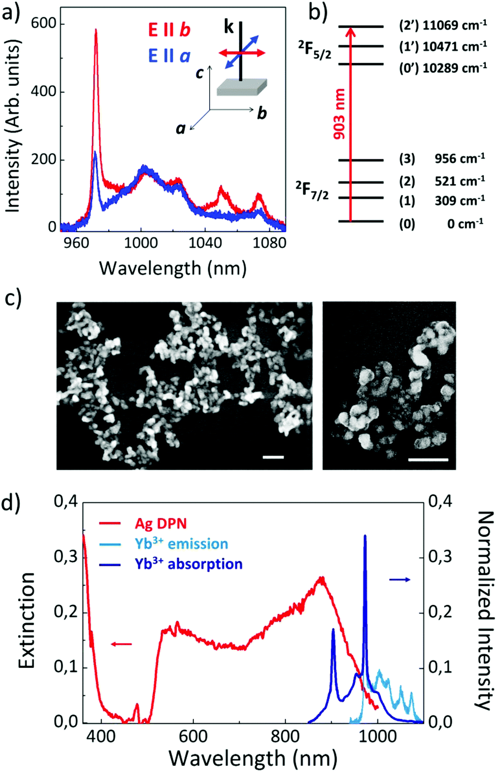 | ||
| Fig. 1 (a) Polarized photoluminescence spectra of Yb3+ ions in RTP: excitation and emission polarized parallel to the a crystal axis (blue spectrum) and to the b crystal axis (red spectrum). The inset depicts the schematic of the configuration used in the experiment. (b) Crystal field energy level scheme of Yb3+ ions in RTP. The excitation transition is indicated by an arrow. (c) SEM image of a large Ag DPN, together with details, obtained by photochemical deposition on the RTP surface. The scale bar in both panels represents 200 nm. (d) Comparison between the extinction spectrum of the Ag DPN (red line) and the normalized absorption and emission spectra (dark and light blue, respectively) of Yb:Nb:RTP obtained for a light beam propagating along the c crystal axis. | ||
According to the C1 point symmetry of the Yb3+ center in RTP, polarization selection rules for the electronic inter-Stark transitions are not expected. Thus, the number and position of the peaks in the spectra are independent of light polarization, as observed in the spectra of Fig. 1a. However, the Stark transition cross-sections vary depending on the polarization direction, which are different for each one of the three orthogonal polarizations parallel to the crystal axis, thus explaining the difference in the relative intensity of the lines in the spectra. On the other hand, the lack of inversion symmetry associated with the C1 point symmetry allows the configuration mixing by the odd crystal field terms. This fact, along with the reported lifetime values for Yb3+ in this system, confirm the dominant character of the forced electric dipole transitions.30
The direct formation of Ag nanostructures on the polar surface of the Yb:Nb:RTP epitaxial layers was achieved by means of the photochemical reduction procedure described in section 2.1. The scanning electron microscopy (SEM) images of the obtained plasmonic structures are shown in Fig. 1c. The left panel displays a low magnification image showing the morphology and extension (up to a few micrometers) of an Ag DPN on a large scale. The right panel shows a detailed view, from which the specific morphology of the Ag NP forming the DPN can be observed. As seen, DPNs are formed by Ag nanoparticles with sizes in the range 60–90 nm connected in a disordered network-like arrangement.
The experimental extinction spectrum of the Ag-DPN is shown in Fig. 1d. It consists of a broad band extending to the NIR with its maximum peak at around 900 nm. This spectrum differs from that obtained for silver nanoparticles, in which the plasmonic response is located in the visible region. The origin of the NIR response in our metallic structures is related to the aggregation of nanoparticles which form the complex structures. As previously reported, for short UV illumination times, the photochemical deposition procedure leads to the formation of nanocubes (2 min) and prism-like shaped Ag nanoparticles (4–8 min) with resonances in the visible spectral region.22,24 For longer times (10 min), the prism-like shaped nanoparticles are connected forming the DPNs. As the illumination time is increased the extinction spectra of the Ag nanostructures broaden and shift to longer wavelengths, from the blue spectral region in the case of isolated nanocubes down to the NIR spectral regions when dealing with DPNs. These latter structures show a certain similarity to percolated systems, in which both the electrical and optical properties display abrupt changes. In particular, the effect of charge delocalization produced by the linking of the isolated NPs after a certain percolation threshold produces a spectral shift of the plasmonic resonance from the visible region to the near-IR.32,33
To illustrate the spectral overlap between the plasmonic response of the Ag DPN and the optical transitions of Yb3+ ions, Fig. 1d also depicts the absorption and emission spectra of Yb3+ in RTP associated with the 2F7/2 ↔ 2F5/2 transition in the 900–1050 nm region. As observed, the absorption of Yb3+ (dark blue line) remarkably overlaps with the plasmonic response of the Ag DPN, particularly the 2F7/2(0) → 2F5/2(2′) Stark transition at 903 nm, which was chosen as the excitation wavelength in this work. Accordingly, resonant interactions between the plasmonic modes supported by the Ag DPN and the transitions of Yb3+ are expected to occur mainly via the excitation, given the smaller overlap of the emission with the DPN extinction spectrum.
3.2 Effect of Ag-DPNs on the Yb3+ photoluminescence
To evaluate the effect of the plasmonic resonance supported by the Ag DPN on the luminescence of Yb3+ ions, we used confocal scanning micro-fluorescence experiments. This technique allows obtaining spatially-resolved spectroscopic images in which the integrated Yb3+ emission spectra are represented as a function of the spatial position on the surface of RTP.Fig. 2a shows as an example a fluorescence map of the integrated Yb3+ emission in the 960–1080 nm spectral range in the vicinity of a DPN. As observed, a well-defined area exhibiting a much stronger photoluminescence signal is clearly distinguished in the central region of the image, where an Ag DPN of around 1.5 μm size is located. Indeed, a systematic increase of the Yb3+ photoluminescence was observed whenever the photoluminescence was analyzed in the proximity of the metallic structures deposited on the RTP surface.
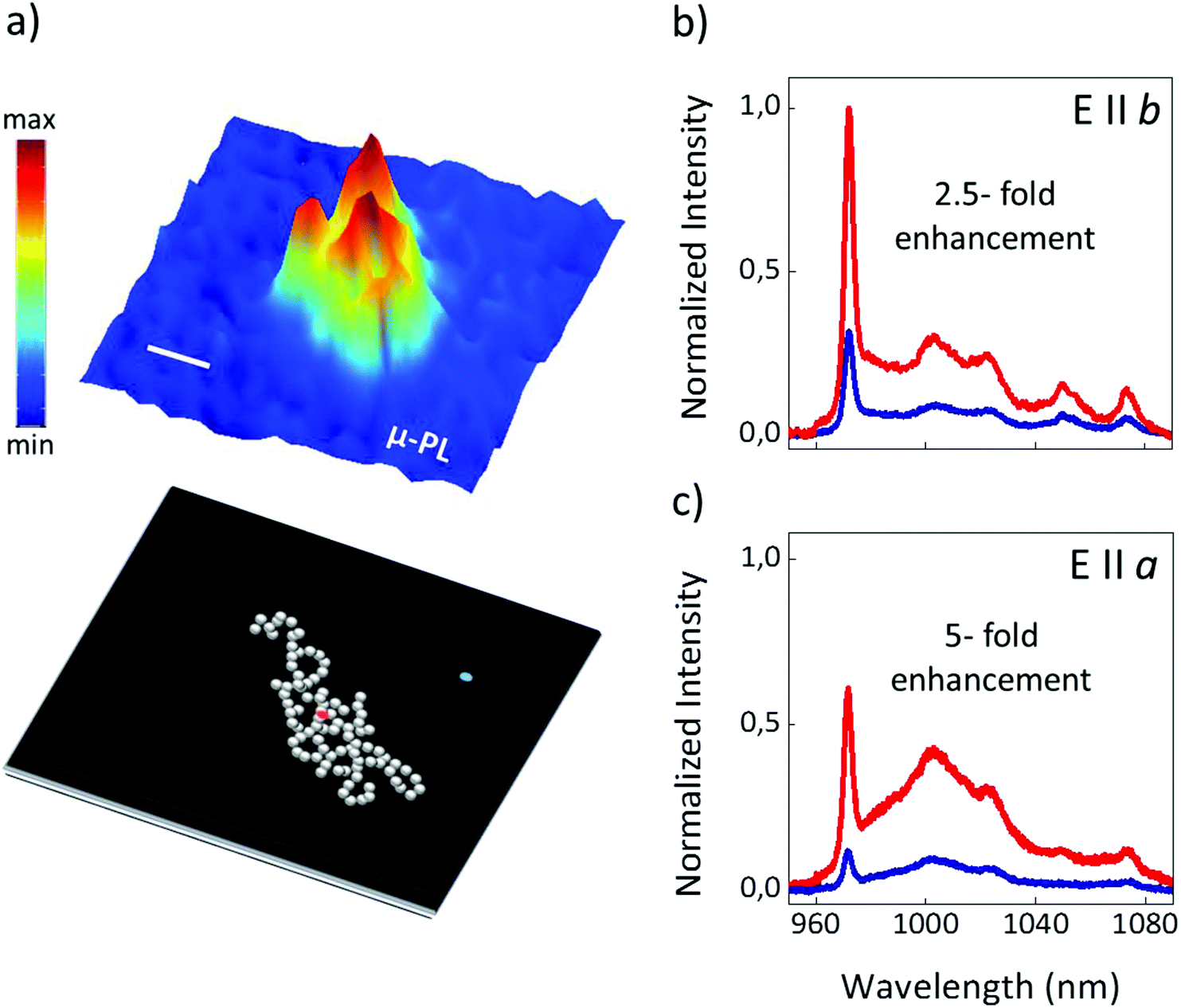 | ||
| Fig. 2 (a) Spatial map of the integrated 2F5/2 → 2F7/2 emission of Yb3+ ions showing the intensification of the photoluminescence in the proximity of a DPN. A schematic view of a DPN photo-deposited on the RTP surface is shown below. Red and blue dots indicate the spatial region where the emission spectra were collected. The scale bar corresponds to 500 nm. (b) and (c) Comparison of the Yb3+ emission spectra in the vicinity (red) and in the absence (blue) of the metallic structures for two different polarization configurations: excitation and emission polarized parallel to the b crystal axis (b) and parallel to the a crystal axis (c). The average values of the enhancement factors are indicated for each configuration. The enhancement factors correspond to the integrated photoluminescence collected in the presence of Ag DPNs divided by that from bare RTP. | ||
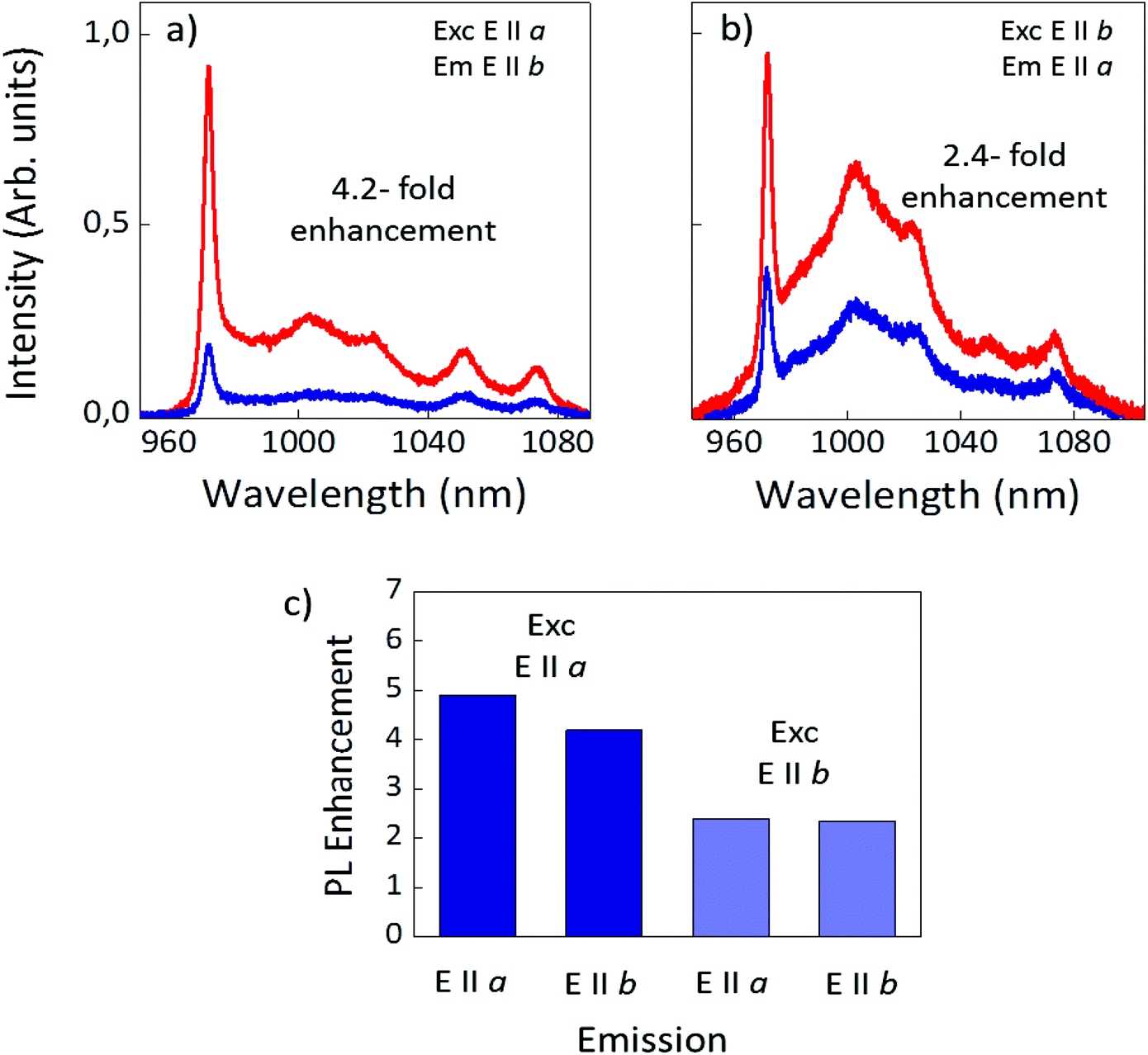
Fig. 2b and c illustrate the anisotropic enhancement of the Yb3+ emission by the Ag DPNs. The figures show two representative examples of the plasmonic enhancement for two different polarization configurations comparing the emission spectra collected in the vicinity of the Ag DPN (red) with those obtained in the absence of Ag structures (blue). The spectra obtained in the absence of the metallic aggregates (blue line) are consistent with those reported for the different polarization configurations in the case of bare RTP, their different shapes and relative intensities being related to the optical anisotropy of the host crystal. In Fig. 2b the polarization of both the excitation and emitted light is parallel to the b crystal axis. As clearly seen, the Yb3+ emission collected from the vicinities of the metallic nanostructures is significantly enhanced. Indeed, an enhancement factor of 2.5 is achieved in this configuration with respect to the case of bare RTP. The enhancement factor is even higher when the polarization of the excitation and the emitted beams are parallel to the a crystal axis (Fig. 2c). In this case, a remarkable enhancement factor of 5 is obtained, which is one of the highest reported for Yb3+ doped crystals emitting in NIR.34,35Fig. 3 provides a further insight into the origin of the plasmonic enhancement of Yb3+ PL in this system. Fig. 3a and b show the Yb3+ photoluminescence spectra in the absence (blue) and in the presence (red) of Ag DPNs for the crossed-polarization configurations, i.e. excitation and emission polarized parallel to the a and b axes, respectively (Fig. 3a) and vice versa (Fig. 3b).
 | ||
| Fig. 3 (a) Yb3+ photoluminescence spectra in the absence (blue) and in the presence (red) of Ag DPNs for excitation and emission parallel to the a and b axes, respectively and (b) for excitation and emission parallel to the b and a axes, respectively. (c) Average enhancement values of the integrated Yb3+ emission in RTP in the vicinities of DPNs for different polarization configurations of the excitation and emission beams. | ||
In both cases the enhancement factors are similar to those obtained in Fig. 2. Fig. 3c summarizes the average enhancement factors obtained for the four cases of interest. As observed, the average enhancement factors are mainly dependent on the polarization of the excitation beam and only slight variations are obtained when analyzing the polarization of the emitted radiation. This result indicates that in our system the photoluminescence enhancement is mainly related to the excitation process.
On the other hand, regarding the emission collected in the vicinity of the Ag DPN, we confirmed that the spectral shape of the Yb3+ emission was not substantially affected by the DPN, which indicates that the forced electric dipole character of the Stark transitions is not altered by the interaction with the metallic nanostructures, similarly to what has been reported in other systems.36Fig. 4 shows the comparison of the Yb3+ normalized emission spectra in the absence and in the presence of metallic structures for two polarization configurations. The shape of the Yb3+ emission spectra is not substantially modified by the presence of the DPN, maintaining the number and relative intensity of the Stark transitions. This is clearly shown in Fig. 4a where the excitation and emitted light are polarized parallel to the b crystal axis (average enhancement factor of 2.5). When the light is polarized parallel to the a axis (average enhancement factor of 5) a slight increase of the 2F5/2(0′) → 2F7/2(0) line at 975 nm with respect to the rest of the spectrum is observed (see Fig. 4b), which suggests a minor coupling of the plasmonic resonance with the Yb3+ emission in agreement with the depolarizing character of the DPN, as is shown below.
 | ||
| Fig. 4 Comparison of Yb3+ emission lineshapes in the vicinity (red) and in the absence (blue) of the metallic structures. Normalized Yb3+ emission spectra obtained when the excitation and emitted light are polarized parallel to the b crystal axis (a) and parallel to the a crystal axis (b). | ||
3.3 Near field distribution analysis
The experimental results can be interpreted by taking into account the near-field response of the Ag DPN together with the anisotropic character of the Yb3+ excitation transitions in the RTP crystal. In general, the photoluminescence enhancement of a certain emitter can be related to the excitation and/or emission enhancement. However, according to the results, in our case we can consider that the dominant mechanism relies on the tuning of the DPN resonance to the Yb3+ excitation, since the Stokes-shifted Yb3+ emission poorly overlaps with the plasmonic response (see Fig. 1d). Therefore, to gain further insight into the experimental results we have performed simulations of the electric field distribution in the near-field regime at the excitation wavelength, λexc = 903 nm. The DPN was modelled by assembling Ag nanoparticles into a network-like arrangement with the spatial morphology observed in the SEM images. The near field distributions were obtained in a plane 5 nm below the surface of the RTP crystal where the DPN was deposited. The results of the calculations are shown in Fig. 5a–c, where the incident beam E0 is characterized by a k vector perpendicular to the a–b crystal plane. Fig. 5a and b show the amplitude of the in-plane near-field components in the directions parallel (E∥E0) and perpendicular (E⊥E0) to the incident field E0, respectively. As observed, the near-field response is very similar for both components in terms of distribution and intensification. Both display some hot-spots as well as broad spatial regions in which the field is enhanced according to the behavior of the DPN. On the other hand, the DPN strongly depolarizes the electric field in the a–b plane, as expected from their morphology, which does not show any preferential directionality. | ||
| Fig. 5 Numerically calculated near field distributions showing the amplitude of the electric field components at 903 nm in a plane 5 nm below the surface of RTP where the Ag DPN was deposited. (a) Near field distribution of the in-plane vector component E∥E0. (b) Near field distribution of the in-plane component E⊥E0. (c) Near field associated with the out-of-plane component Ez∥k. The white scale bar corresponds to 50 nm. (d), (e) and (f) Absorption cross-section spectra associated with the 2F7/2(0) → 2F5/2(2′) Stark transition of Yb3+ in RTP for different orientations of the incident beam with respect to the crystal axis: E∥a, E∥b, and E∥c, respectively. | ||
A relevant feature in the context of this work is the presence of an out-of-plane polarization component (hereafter Ez) in addition to those of the incident field, which appears in the near-field regime due to the presence of the Ag aggregates (see Fig. 5c). Moreover, as observed in Fig. 5c, the largest values of the local field enhancement correspond to the z field component. Hence, according to the simulations, the near field in the vicinity of the plasmonic networks dominantly points along the c crystal direction. Therefore, even if the out-of-plane Ez component is not accessible in our far field experimental configuration, it constitutes the major near-field contribution to the Yb3+ excitation enhancement. The presence of additional out-of-plane near field components is expected since plasmonic structures change the near-field distribution and polarization.37
4. Discussion
Considering that the enhanced photoluminescence is mainly due to the excitation enhancement of Yb3+ ions, the results can be analyzed taking into account the excitation rate enhancement of the emitter which can be expressed as:38 | (1) |
To correlate the amplitude of the near field components with the photoluminescence enhancement observed for the different polarizations (Fig. 2b and c), the Yb3+ transition dipolar moments along the different crystal directions have to be considered. These are directly related to the Yb3+ absorption cross-section of the involved transition. Fig. 5d–f show the absorption cross-section spectra of Yb3+ at the relevant excitation wavelength (903 nm, 2F7/2(0) → 2F5/2(2′) Stark transition) for different polarization configurations obtained in the absence of plasmonic networks. The absorption cross-section values at the maxima are σa = 0.15 × 10⁻²⁰ cm2 (E∥a), σb = 0.22 × 10⁻²⁰ cm2 (E∥b), and σc = 0.57 × 10⁻²⁰ cm2 (E∥c), the most intense absorption occurs when the electric field of the light is parallel to the c crystal axis.
In the case of Yb3+ doped RTP epitaxial layers in the absence of Ag DPNs, the excitation rates associated with the electric field vector E0 parallel to the a and b crystal axes are given by pa2|E0|2 and pb2|E0|2, respectively. In the presence of Ag DPNs, the electric field intensity is enhanced by a local field enhancement factor g = E/E0, which shows the highest value (gz) for the Ez component according to the near field distribution of Fig. 5. This Ez component constitutes the major near-field contribution to the amplitude. Moreover, the Ez component allows access to the transition dipole moment along the c direction, pc, which according to the Yb3+ absorption cross-section shows the strongest value (Fig. 5f). Thus, considering the dominant role of both the near field amplitude of the Ez component and the intensity of the dipole transition along the c direction, in the presence of our metallic structures the excitation rate can be approximated by pc2|gzE0|2. Consequently, according to (1), the excitation rate enhancement of the Yb3+ ions in the vicinity of the Ag DPN can be written as:
 | (2) |
5. Conclusions
The optical properties of disordered plasmonic networks self-assembled on the polar surface of RTP ferroelectric crystals have been exploited to demonstrate an exceptional 5-fold photoluminescence enhancement of Yb3+, a technologically relevant laser ion operating in the NIR. We demonstrate that the dominant mechanism is related to the Yb3+ excitation enhancement due to the tuning of the metallic nanostructure resonance to the Yb3+ absorption. We show that in the near field regime, the presence of the metallic structures generates an out-of-plane polarization component Ez, which not only constitutes the major near-field contribution to the amplitude, but also allows access to the largest transition dipolar moment of Yb3+ ions in RTP. As a result, a much more efficient route for Yb3+ excitation takes place at the immediacy of the metallic networks.This work provides fundamental insights for tailoring metallic nanoparticle arrangements to enhance the optical properties of Yb3+ ions, and paves the way for increasing the excitation rate of other RE ion emitters with absorption bands in the NIR spectral region. In particular, the results offer an alternative route for the selective enhancement of RE transitions with specific polarization character without the need for carefully engineered structures. Because of the key role played by Yb3+ ions as sensitizers in energy transfer up-conversion processes, the possibility to enhance the excitation rate in the near infrared region provides interesting routes for increasing the efficiency of the process as desired in several technological applications including sensing, solar energy conversion and biological imaging, among others. Finally, this work constitutes a promising step towards the development of new multifunctional Yb3+-based plasmon assisted solid-state lasers operating at the nanoscale.
Acknowledgements
This work has been supported by the Spanish Ministry of Economy and Competitiveness (MINECO) under projects MAT-2016-76106-R, MAT2013-43301-R, MAT2016-75716-C2-1-R and TEC2014-55948-R. The authors also acknowledge Comunidad de Madrid under grant S2013/MIT-2740 and Generalitat de Catalunya under grant SGR2014SGR1358. LSG acknowledges FPU13/02476 grant from the Spanish Ministry of Education. C. T. was supported by funding from the People Programme (Marie Curie Actions) of the European Union's Seventh Framework Programme (FP7/2007-2013) under REA grant agreement number 609405 (COFUNDPostdocDTU).References
- L. Novotny and N. Van Hulst, Nat. Photonics, 2011, 5, 83 CrossRef CAS.
- S. Butun, S. Tongay and K. Aydin, Nano Lett., 2015, 15, 2700 CrossRef CAS PubMed.
- R. F. Oulton, V. J. Sorger, T. Zentgraf, R.-M. Ma, C. Gladden, L. Dai, G. Bartal and X. Zhang, Nature, 2009, 461, 629 CrossRef CAS PubMed.
- L. Tang, S. E. Kocabas, S. Latif, A. K. Okyay, D.-S. Ly-Gagnon, S. Saraswat and D. A. B. Miller, Nat. Photonics, 2008, 2, 226 CrossRef CAS.
- J. N. Anker, W. P. Hall, O. Lyandres, N. C. Shah, J. Zhao and P. Van Duyne, Nat. Mater., 2008, 7, 442 CrossRef CAS PubMed.
- A. Gómez-Tornero, C. Tserkezis, L. Mateos, L. E. Bausá and M. O. Ramírez, Adv. Mater., 2017, 29, 1605267 CrossRef PubMed.
- R.-M. Ma, R. Oulton, V. J. Sorger and X. Zhang, Laser Photonics Rev., 2013, 7, 1 CrossRef CAS.
- Q. Zhang, G. Li, X. Liu, F. Qian, Y. Li, T. C. Sum, C. M. Lieber and Q. Xiong, Nat. Commun., 2003, 5, 4953 CrossRef PubMed.
- X. Wu, Y. Xiao, C. Meng, X. Zhang, S. Yu, Y. Wang, C. Yang, X. Guo, C. Z. Ning and L. Tong, Nano Lett., 2013, 13, 5654 CrossRef CAS PubMed.
- P. Molina, E. Yraola, M. O. Ramírez, C. Tserkezis, J. L. Plaza, J. Aizpurua, J. Bravo-Abad and L. E. Bausá, Nano Lett., 2016, 16, 895 CrossRef CAS PubMed.
- J. J. Carvajal, G. Ciatto, X. Mateos, A. Schmidt, U. Griebner, V. Petrov, G. Boulon, A. Brenier, A. Peña, M. C. Pujol, M. Aguiló and F. Díaz, Opt. Express, 2010, 18, 7228 CrossRef CAS PubMed.
- G. Bai, M. K. Tsang and J. Hao, Adv. Funct. Mater., 2016, 26, 6330 CrossRef CAS.
- B. Zhou, B. Shi, D. Jin and X. Liu, Nat. Nanotechnol., 2015, 10, 924 CrossRef CAS PubMed.
- A. Foucault-Colleta, K. A. Gogickb, K. A. Whiteb, S. Villettea, A. Palliera, G. Colleta, C. Kiedaa, T. Lib, S. J. Geibb, N. L. Rosib and S. Petouda, Proc. Natl. Acad. Sci. U. S. A., 2013, 110, 17199 CrossRef PubMed.
- F. Vetrone, R. Naccache, A. Juarranz de la Fuente, F. Sanz-Rodriguez, A. Blazquez-Castro, E. Martin-Rodriguez, D. Jaque, J. García-Solé and J. A. Capobianco, Nanoscale, 2010, 2, 495 RSC.
- B. M. van der Ende, L. Aarts and A. Meijerink, Adv. Mater., 2009, 21, 3073 CrossRef CAS.
- Y. Tang, W. Di, X. Zhai, R. Yang and W. Qin, ACS Catal., 2013, 3, 405 CrossRef CAS.
- B. Denker and E. Shklovsky, Handbook of solid-state lasers, Materials, systems and applications, Woodhead Publishing, 2013 Search PubMed.
- J. Hao, Y. Zhang and X. Wei, Angew. Chem., Int. Ed., 2011, 50, 6876 CrossRef CAS PubMed.
- M. Shalaev, C. X. Ying, Z. Zhang and H. Cao, Phys. Rev. Lett., 2006, 97, 206103 CrossRef PubMed.
- S. V. Kalinin, D. A. Bonnell, T. Alvarez, X. J. Lei, Z. H. Hu, R. J. Shao and H. Ferris, Adv. Mater., 2004, 16, 795 CrossRef CAS.
- L. Sánchez-García, M. O. Ramírez, P. Molina, F. Gallego-Gómez, L. Mateos, E. Yraola, J. J. Carvajal, M. Aguiló, F. Díaz, C. de las Heras and L. E. Bausá, Adv. Mater., 2014, 26, 6447 CrossRef PubMed.
- H. Karlsson, F. Laurell and L. K. Cheng, Appl. Phys. Lett., 1999, 74, 1519 CrossRef CAS.
- L. Sánchez-García, C. Tserkezis, M. O. Ramírez, P. Molina, J. J. Carvajal, M. Aguiló, F. Díaz, J. Aizpurua and L. E. Bausá, Opt. Express, 2016, 24, 8491 CrossRef PubMed.
- H. Mertens, J. S. Biteen, H. A. Atwater and A. Polman, Nano Lett., 2006, 6, 2622 CrossRef CAS PubMed.
- P. Molina, E. Yraola, M. O. Ramirez, J. L. Plaza, C. Heras and L. E. Bausa, Nano Lett., 2013, 13, 4931 CrossRef CAS PubMed.
- J. Cugat, R. M. Solé, J. J. Carvajal, M. C. Pujol, X. Mateos, F. Díaz and M. Aguiló, CrystEngComm, 2011, 13, 2015 RSC.
- J. J. Carvajal, V. Nikolov, R. Solé, J. Gavaldà, J. Massons, M. Aguiló and F. Díaz, Chem. Mater., 2002, 14, 3136 CrossRef CAS.
- E. D. Palik, Handbook of Optical Constants of Solids, Academic Press, 2002 Search PubMed.
- A. Peña, J. J. Carvajal, M. C. Pujol, X. Mateos, M. Aguiló, F. Díaz, V. Petrov, P. Segonds and B. Boulanger, Opt. Express, 2007, 15, 14580 CrossRef.
- A. Lupei, V. Lupei, V. N. Presura and A. Petraru, J. Phys.: Condens. Matter, 1999, 11, 3769 CrossRef CAS.
- A. A. Earp and G. B. Smith, J. Phys. D: Appl. Phys., 2011, 44, 255102 CrossRef.
- A. I. Maaroof and D. S. Sutherland, J. Phys. D: Appl. Phys., 2010, 43, 405301 CrossRef.
- Y. Lu and X. Chen, Appl. Phys. Lett., 2009, 94, 193110 CrossRef.
- V. A. G. Rivera, Y. Ledemi, M. A. Pereira-da-Silva, Y. Messaddeq and E. Marega Jr., Sci. Rep., 2016, 6, 18464 CrossRef CAS PubMed.
- E. Yraola, P. Molina, J. L. Plaza, M. O. Ramírez and L. E. Bausá, Adv. Mater., 2013, 25, 910 CrossRef CAS PubMed.
- M. Schnell, A. Garcia-Etxarri, J. Alkorta, J. Aizpurua and R. Hillenbrand, Nano Lett., 2010, 10, 3524 CrossRef CAS PubMed.
- S. Derom, A. Berthelot, A. Pillonnet, O. Benamara, A. M. Jurdyc, C. Girard and G. Colas des Francs, Nanotechnology, 2013, 24, 495704 CrossRef CAS PubMed.
| This journal is © The Royal Society of Chemistry 2017 |