
 Open Access Article
 This Open Access Article is licensed under a Creative Commons Attribution-Non Commercial 3.0 Unported Licence
Low-temperature crystallization of solution-derived metal oxide thin films assisted by chemical processes†
Iñigo
Bretos
 *,
Ricardo
Jiménez
,
Jesús
Ricote
and
M. Lourdes
Calzada
*
*,
Ricardo
Jiménez
,
Jesús
Ricote
and
M. Lourdes
Calzada
*
Instituto de Ciencia de Materiales de Madrid (ICMM-CSIC), Sor Juana Inés de la Cruz 3, E-24089 Madrid, Spain. E-mail: ibretos@icmm.csic.es; lcalzada@icmm.csic.es
First published on 22nd November 2017
Abstract
Over the last few years the efforts devoted to the research on low-temperature processing of metal oxide thin films have increased notably. This has enabled the direct integration of metal oxide layers (amorphous semiconductors) on low-melting-point polymeric substrates for flexible electronic systems, which adds to the economic and environmental benefits of the use of these processes with reduced energy consumption. More challenging is the preparation of crystalline complex oxide films at temperatures compatible with their direct integration in flexible devices. However, the usually high crystallization temperatures (>600 °C) impede the development of devices that take full advantage of the large variety of oxide functionalities available. This tutorial review analyzes a number of strategies based on wet chemical methods for inducing the crystallization of metal oxide thin films at low temperatures. The key mechanisms are explained in relation to the specific step of the fabrication process reached in an earlier stage: the formation of a defect-free, highly densified amorphous metal–oxygen network or the actual crystallization of the metal oxide. The role of photochemistry, where light can be used as a complementary energy source to induce crystallization, is particularly highlighted. This requires the synthesis of novel photosensitive solutions (modified metal alkoxides, charge-transfer metal complexes or structurally designed molecular compounds) and a precise control over the reactions promoted by UV irradiation (photochemical cleavage, ozonolysis, condensation or photocatalysis). Relevant examples derived from the integration of crystalline metal oxide thin films on flexible substrates (≤350 °C) illustrate the most recent achievements in this field.
 Iñigo Bretos | Iñigo Bretos is currently a ComFuturo Researcher at the Materials Science Institute of Madrid (ICMM-CSIC). He received his PhD degree in Chemistry from Universidad Autónoma de Madrid (Spain) in 2006. Then he joined RWTH Aachen University (Germany) with a postdoctoral position. His research interests encompass materials science and technology, with a focus on the processing and integration of functional oxide layers (ferroelectrics, piezoelectrics, dielectrics, multiferroics or superconductors) in advanced electronics and emerging technologies for applications ranging from memory devices and transduction to photovoltaics and flexible systems. Recently (2017), he was awarded a Ramón y Cajal fellowship. |
 Ricardo Jiménez | Ricardo Jiménez received his PhD in Chemistry from Universidad Autónoma de Madrid (Spain) in 1994. He made a postdoctoral stay at the Laboratoire de electrochimie et physico-chimie of solids and interfaces in Grenoble (France). Then he joined the Materials Science Institute of Madrid (ICMM-CSIC) in 1997. Since 2005, he is Tenured Scientist. The formation in solid-state electrochemistry joined with his experience in ferroelectric materials characterization contribute to his wide expertise in the functional characterization of electro-ceramics in both bulk and thin film forms. Besides, he has a long experience in preparation and physical properties of composite materials and thermo-mechanical properties. |
 Jesús Ricote | Jesús Ricote received his PhD degree in Physics from Universidad Complutense de Madrid (Spain) in 1994. After a short postdoctoral stay at the Centre d’Elaboration et des Études Estructurales de Materiaux, CNRS (Toulouse. France) in 1995, he joined the Nanotechnology Group of Cranfield University (United Kingdom) as research officer (1996–1998). Later he obtained a postdoctoral fellowship (1998–1999) at the Univ. du Maine-Le Mans (France). In 1999 he joined the Materials Science Institute of Madrid (CSIC) and became Tenured Scientist in 2007. His research interests include the quantitative microstructural analysis of ferroelectric polycrystalline materials with XRD, electron and scanning force microscopies. |
 M. Lourdes Calzada | M. Lourdes Calzada obtained her PhD degree in Chemistry from Universidad of Alcalá (Spain) in 1990. After a postdoctoral fellowship at the School of Materials of the University of Leeds (United Kingdom), she joined the Materials Science Institute of Madrid (ICMM-CSIC), where she was appointed to Research Professor in 2010. Her research interests are focused on the development of low-temperature sol–gel synthesis strategies to attain metal oxides and the integration of functional films in micro and flexible electronics. She is author of more than 175 publications, multiple international conferences, 9 book chapters and co-inventor in 3 patents. |
Key learning points(1) Key strategies to promote the metal oxide formation and crystallization in thin films prepared by wet chemical methods.(2) Solution chemistry for designing “à la carte” molecular precursors. (3) Light as an alternative energy source to induce crystallization of metal oxide thin films by photochemistry. (4) Integration of metal oxides in electronic devices, especially flexible systems. (5) Environmental, economic, and technological implications of the low-temperature processing of advanced materials. |
1. Introduction
Heating (and cooling) accounts for around 70% of the energy consumed in the manufacturing process of a product. Electronics is not an exception, and the energy required to fabricate many of the active electronic components present in consumer products (e.g. smartphones, tablets or laptops) lies well above that of other more conventional manufacturing processes. For example, the thermal oxidative processes used in microelectronics for semiconductor oxide layers require an energy input up to six orders of magnitude higher than the minimum work needed in metalworking to melt aluminum or iron for casting (∼1 MJ kg−1).1 Therefore, the ever increasing demand of electronics makes the reduction of the energy consumption during their processing unavoidable for a sustainable and competitive manufacturing industry worldwide. This has pushed the research community to explore alternative fabrication processes with much lower heating demands that can efficiently substitute the traditional thermal annealing of most electronic materials at elevated temperatures.2–5 The benefits obtained from decreasing the processing temperature span from minimizing the environmental impact (carbon footprint) to reducing the overall costs of the production line. This is much related to the principles of the so-called “green chemistry”, where the use of low temperatures and mild conditions is specifically pursued in the synthesis of advanced materials.Besides the aforementioned ecological and economic benefits, the low-temperature processing has also opened the door to the incorporation of an increasing number of materials in technologically disruptive areas like flexible electronics.6 This is the case of metal oxides, a superb class of inorganic materials that introduces an unprecedented wealth of functionalities (electrical, magnetic or optical) to the existing flexible devices. Thin films of metal oxides are consequently at the forefront of current and next-generation devices, where systems supported on low-cost, lightweight, and flexible substrates are expected to revolutionize the electronic industry by new applications such as large-area displays, wearable sensors, smart textiles or electronic skin. Nowadays, the direct growth of metal oxide layers on low-melting-point flexible substrates (e.g. plastic, paper, or textile) is only possible at processing temperatures below the thermal degradation of the latter: around 350 °C in the most favorable case (i.e. polyimide foils). This constitutes a big challenge for the effective integration of multifunctional metal oxides, since their crystallization temperatures (usually over 600 °C) are still several hundred degrees above the values that polymeric substrates can withstand. If crystallization is not achieved, most metal oxides lack of the physical property that ultimately defines the functionality of the material. The strong electronic correlations imposed by the crystal lattice usually rule the behavior of complex transition metal oxides.7 For example, crystalline oxides with the perovskite structure (ABO3, where A and B stand for different metal atoms) show correlations between the electrons of neighboring atoms that lead to ferroelectricity (BaTiO3, PbZr1−xTixO3), multiferroicity (BiFeO3, BiMnO3), high-temperature superconductivity (YBa2Cu3O7), or ferromagnetism (La1−xSrxMnO3). Other oxides show adequate properties in the amorphous state, like post-transition metal oxide semiconductors (Zn–Sn–O, In–Zn–O and In–Ga–Zn–O systems). Indeed, their electronic performance improves drastically with the formation of a defect-free, highly densified metal–oxygen network, which is actually the very prelude to the crystallization.8 Therefore, any advance in the crystallization process of metal oxide thin films during low-temperature processing results crucial for their successful integration in next-generation flexible electronics.
The processes leading to crystallization are in many ways governed by chemistry. In this review we present a selection of the most relevant chemical methodologies currently employed to induce the crystallization of metal oxide thin films at low temperatures, revealing tips and tricks used to this aim. Special attention is paid to photochemistry, since light can be used as a complementary energy source to induce crystallization at much more moderate temperatures. Finally, recent applications in devices resulting from the direct integration of crystalline metal oxides on flexible polymeric substrates are highlighted.
2. Low-temperature chemical methods
The fabrication temperature of metal oxides is strongly dependent on both the material system (i.e. chemical composition) and form (e.g. nanoparticles, single crystals, bulk ceramics, thin films). Concerning this last point, before metal oxides were prepared in thin film form almost all of the current compositions had their beginnings in the bulk materials. Therefore, the high sintering temperatures normally used in the well-established ceramic method (far exceeding a thousand degrees Celsius) can serve as the reference for the processing temperatures initially required for these oxides. During the past several decades chemical methods that lower these temperatures have been searched. Since the 1950s, a series of sintering techniques (e.g. hot pressing, flash sintering, microwave sintering, or spark plasma sintering) was developed with the aim of increasing the driving force for densification of the bulk ceramic. While these methods actually led to a decrease in the temperature of the process, the values obtained (over 900 °C) were still too high to enable the incorporation of metal oxides in applications where other components are compromised by them (e.g. microelectronics). Recently, a method called “cold sintering process” (CSP) has allowed the fabrication of a wide range of bulk ceramics (including metal oxides) between room temperature and 200 °C at high uniaxial pressures (50–500 MPa).9 The chemical strategy consists in the use of water as a transient solvent that rapidly evaporates, enabling the supersaturation of the liquid phase employed as an intermediate agent during sintering. The CSP technique is actually based on the hydrothermal synthesis, a widely used chemical method to crystallize compounds from solution media using large pressures for very long times (usually days) in an autoclave.10 Therefore, it is remarkable the important role played by the liquid phases in these low-temperature chemical methods applied to bulk materials.The irruption of the semiconductor industry around 1960 promoted an intensive research in thin film electronics, making possible the integration of metal oxides in microelectronic devices by their deposition as layers onto a substrate (mainly, silicon). To form the metal oxide thin film, deposition methods based on chemical processes proceed by reactions in either vapor or liquid phase. This results in a lower activation energy (via thermal treatment) for the effective mass transport of reactants compared to the rate limiting step of solid-state diffusion (>1000 °C), as it was demonstrated before for bulk ceramics. But as a major difference to the conventional ceramic method—where the bulk material is finally consolidated by sintering at the maximum temperature—the full crystallization of the metal oxide film is now the final step of the fabrication process. Metal oxides in thin-film form are conventionally crystallized at around 800 °C. Although this temperature may vary as a function of the composition, it is always above several hundred °C for most electronic metal oxide films. Thus, this becomes the reference temperature for the low-temperature processing of these films by chemical methods.
Among the crystallization methods in vapor phase used for the fabrication of metal oxide thin films, chemical vapor deposition (CVD) is a mature technology with significant success in the manufacturing of electronic semiconductors since the 1970s.11 Most CVD processes are based on the thermal decomposition of gaseous precursors after chemical reaction on or nearby a heated substrate to yield a fully crystalline material. In the last decades several variants have been developed to reduce the temperature of the process, such as metalorganic chemical vapor deposition (MOCVD). The use of metalorganic precursors instead of conventional halides or hydrides results in a temperature decrease of several hundreds of degrees Celsius (temperatures down to 500 °C) owing to the lower decomposition temperatures of the former. Additionally, once these vapor precursors are adsorbed on a surface they may undergo complementary chemical reactions with other reactive partners (e.g. hydrolysis induced by water vapor) to form the desired material at still lower temperatures (below 500 °C). This is the basis of atomic layer deposition (ALD), which proceeds via alternating exposure of chemical precursors to crystallize the final compound layers. Another alternative is the use of a reactive plasma (i.e. using electron energy as activation method) in the plasma-enhanced chemical vapor deposition (PECVD) that enhances the rate of the reactions and leads to the crystallization of metal oxide thin films at temperatures below 500 °C. In the last few years, low-temperature atmospheric pressure plasma processes (AP-PECVD) have gained momentum due to additional advantages, such as the non-dependence on expensive vacuum systems and the possibility of using continuous, in-line processing at temperatures even below 250 °C.12
A considerable number of low-temperature processes for the crystallization of metal oxide thin films came up from liquid phase approaches, which set the basis of chemical solution deposition (CSD) methods. The origins of this methodology are attributed to the development of soft-chemistry routes in the early 1980s. This original French term (“chimie douce”) refers to a new concept for the synthesis of inorganic and hybrid materials by molecular engineering, using reactions occurring at mild conditions (e.g. low temperatures) in a solution medium.13 In essence, these methods are based on the hypothesis that the molecular homogeneity of the starting liquid precursor is preserved in the final crystalline material. The ability of tailoring the properties of the metal oxide thin films by modifications of the precursor solution chemistry constitutes the main advantage of soft-chemistry routes over vapor-phase reactions. Sol–gel can be considered the flagship of soft-chemistry routes. It involves the use of several types of molecular precursors, usually metal salts and alkoxides, that undergo controlled reactions of hydrolysis and polycondensation forming an interconnected polymeric network of metal centers via oxo- or hidroxo-bridges when in solution at moderate temperatures.14 A crystalline film is obtained after the complete decomposition of the organic matrix after deposition, achieved by a thermal treatment in the relatively low-temperature range of 700–500 °C. In addition to the standard hydrolytic processes, alternative non-hydrolytic sol–gel routes have been developed during the last decades, and have become powerful methodologies for the crystallization of metal oxides at similar temperatures.15 Their peculiarity lies in the use of organic oxygen-donors (e.g. alcohols, ethers, carboxylic acids, ketones, alkoxides) instead of water to promote the condensation reactions at a comparatively slower rate, which favors the controlled crystallization of the metal oxide with a one-step route. More recently, the combination of wet-chemistry routes with microwave and laser heating, or with light-induced reactions, has reduced the processing of metal oxide thin films to impressive low temperature limits (down to 200 °C). These non-conventional, advanced chemical solution deposition (a-CSD) methods have also opened novel crystallization pathways to be explored in the synthesis of these materials, which will be detailed in the present review.
The ever increasing demand for low-cost and energy efficient manufacturing processes, together with the pressing need for new materials and devices in emerging technologies, is driving recent research efforts towards the near-room-temperature processing of metal oxide thin films using chemical methods. This is clearly inferred from Fig. 1, where a summary of the crystallization temperatures used over the last few decades for thin films of typical metal oxides (magnetic, superconducting, conducting, semiconducting, dielectric, ferroelectric, piezoelectric, or multiferroic) is shown. Whereas both vapor and liquid-based methods show the general trend of lowering the processing temperatures over the years, comparatively lower temperature limits are achieved by the latter for the important family of functional multimetal oxides. This can be attributed to the large versatility of the liquid-phase approaches, which allows further exciting developments in this field, as it will be described in the following section.
 | ||
| Fig. 1 Summary in chronological order of the temperature ranges typically used for crystallization of several metal oxide thin films with regard to different chemical methods of fabrication (CSD = chemical solution deposition, a-CSD = advanced chemical solution deposition, MOCVD = metalorganic chemical vapor deposition, ALD = atomic layer deposition, PECVD = plasma-enhanced chemical vapor deposition, AP-PECVD = atmospheric pressure plasma-enhanced chemical vapor deposition). Data are compiled from the open literature (corresponding references are listed in ESI,† Fig. S1). YBCO = YBa2Cu3O7, PLT = (Pb,La)TiO3, PTO = PbTiO3, PZT = Pb(Zr,Ti)O3, SBT = SrBi2Ta2O9, LNO = LaNiO3, LMO = LaMnO3, BST = (Ba,Sr)TiO3, SRO = SrRuO3, BFO = BiFeO3, STO = SrTiO3, BTO = BaTiO3, ITO = In–Sn–O, BiT = Bi4Ti3O12, NBT = (Na,Bi)TiO3, KNN = (K,Na)NbO3. | ||
3. Solution deposition of metal oxide thin films
A metal oxide film is a solid material supported onto a substrate that has oxygen anions chemically bonded to one or more metal cations. The solid can be built either by a disordered metal–oxygen network (i.e. the amorphous oxide) or by the metal and oxygen ions arranged in a highly ordered structure that extends in all directions forming a crystal lattice (i.e. the crystalline oxide).16 Differentiating the mechanisms that lead to one state or another in the material is crucial to understand the keys for the low-temperature processing of metal oxide thin films.Chemical solution deposition (CSD) is a low-cost method that scales easily to large areas without complex manufacturing systems. Fig. 2 shows the main steps of this fabrication technique, together with the structural evolution of the material during the process. In the first stage (stage i), a precursor solution is obtained by the reaction among metal reagents, solvents and other chemicals (e.g. catalysts).14 The deposition of this solution on a substrate leads to a wet layer (stage ii), where a rapid evaporation of the solvent prevents entanglement and favors densification against condensation. Densification in this layer occurs by viscoelastic flow, always faster than the densification by solid-state diffusion that occurs in rigid layers. Annealing of the wet layer is thus required for the evaporation of low-boiling-point compounds (e.g. trapped solvent) and decomposition of the metal precursors, as well as for promoting the hydrolysis and condensation reactions with the subsequent formation of oxo-bridges among the metal cations. If small particle inclusions (e.g. precipitates, intermediate phases) are formed before porosity and organic residuals are totally removed, the densification rate of the amorphous layer will be reduced. So rapid but long heat treatments are usually needed for full densification. Ultimately, the wet layer is transformed into a rigid solid constituted by an amorphous metal–oxygen network (stage iii).14 Here, a close packing of the metal and oxygen atoms with short diffusion distances facilitates the conversion to the final crystalline metal oxide film (stage iv). This means that a metal–oxygen network with an arrangement of the atoms resembling that of the crystal structure can be crucial to bring down the crystallization temperature of the film. The thermodynamic barrier between this ideal amorphous film and the crystalline one would be so small that it could be easily surpassed by supplying a small amount of energy.
 | ||
| Fig. 2 Diagram showing the main steps (I–IV) of CSD together with the different stages (i–iv) reached in the material during its evolution from the initial precursor solution to the final crystalline film. | ||
In the so-called conventional processing, the formation and crystallization of the metal oxide thin film usually take place at temperatures between 200–400 °C (stage III) and above 600 °C (stage IV), respectively. Here, we will review the keys to reduce them until the crystallization is carried out below 400 °C in the low-temperature processing of these materials by CSD.
3.1 Fundamental concepts
In order to find the key aspects that will allow decreasing the processing temperatures, we need to revise the fundamentals behind each step of the CSD of metal oxide thin films (see Fig. 2). The first one concerns the synthesis of a stable solution that must contain all the metal cations in the desired stoichiometric ratio (step I). Table 1 summarizes the characteristics of each of the most frequently used chemical routes to obtain precursor solutions of metal oxides, including some new promising approaches.13,17–21 Once the precursor solution is synthesized, a thin layer is deposited (step II) onto a substrate by any of the variety of coating techniques available (Fig. 3).16 Among them, dip-coating, spin-coating, spray-coating or inkjet printing are large-area deposition techniques commonly used for precursor solutions of single and multimetal oxides. The rest of the techniques included in Fig. 3 also have successfully been used, but mainly for the deposition of layers of single oxides. After the coating of the substrate, several phenomena occur that are overlapped. These are the drying of the wet layer by the evaporation of the low-boiling point chemicals, and the subsequent pyrolysis of the organic compounds and condensation of the metal precursors (step III). Thermal annealing is applied to the sample during this third step at relatively low temperatures, which is usually carried out on a hot plate. The last step is the crystallization of the amorphous film, which is traditionally carried out by thermal treatment at high temperatures (step IV). We can distinguish two types of thermal annealing: conventional furnace annealing (CFA) and rapid thermal annealing (RTA). CFA uses heating rates of several degrees Celsius per minute, whereas RTA uses heating rates that are several degrees Celsius per second. The latter is the process conventionally used in the microelectronic industry because it minimizes the diffusion reactions between film and substrate, avoids the stabilization of intermediate phases and enhances the film densification. Finally, it must be considered that to obtain the desired film thickness, multiple deposition and pyrolysis is usually required. The microstructure and crystallographic orientation of the films can be affected whether a layer-by-layer crystallization process or alternative one-step crystallization is followed.| Chemical system | Solution features | Film features and issues | |
|---|---|---|---|
| Sol–Gel14,16,17 |
Alkoxide route; applied to transition and post-transition metal oxide films
Solvents: alcohols (e.g., methoxyethanol) Reagents: metal alkoxides |
High rates of hydrolysis and condensation reactions
– Synthesis in inert gas – Solutions not stable in air. |
High control of the film homogeneity and stoichiometry |
| Chelate route16,17 |
Modification of alkoxide route; applied to films of transition and post-transition metal oxides, and alkaline and alkaline earth oxides
Solvents: alcohols and non-interacting liquids Reagents: metal alkoxides stabilized with polar groups, inorganic metal salts or metal carboxylates |
Reduction of the hydrolysis and condensation reactions
– Synthesis in air – Solutions stable in air – Diminished control of solution rheology |
Moderate control of the film homogeneity and stoichiometry |
| Metal organic decomposition (MOD)16,17 |
Applied to films of transition and post-transition metal oxides, and oxides of low valent ionic cations (e.g., Pb2+, Sr2+, Ba2+)
Solvents: (short alkyl chain) water, polar solvents (long alkyl chain) non-polar solvents Reagents: metal carboxylates, metal alkoxides |
Simple solution chemistry
– No reaction among the metal reagents and the solvent – Air-stable solutions |
Reduced control of homogeneity and stoichiometry |
| Nitrate, citrate, Pechini routes16,17 |
Applied to films of most metal oxides
Solvents: water, alcohols citric acid, ethylene glycol Reagents: metal nitrates of most metals |
Simple solution preparation
– Air-stable solutions – Diminished control of solution rheology |
Appearance of cracks
Wetting problems Recrystallization of the starting reagents |
| Aqueous solution–gel16,17 |
Applied to films of most metal oxides
Solvents: water, chelating carboxylic acids, ethylenediamine, hydrogen peroxide Reagents: inorganic metal salts, water-soluble metal complexes |
Inexpensive, ecological
– Easy handling of the reagents and solutions in air |
Wetting problems |
| Molecular precursors19 |
Applied to films of earth, transition, post-transition, lanthanide oxides
Solvents: alcohols, diols, triols, alkanolamines, hydrofluoric acid Reagents: metal alkoxides, carboxylates, halides, alkyls or metal β-diketonates, zerovalent metals Applied to: metal oxides of alkaline, alkaline |
Structurally designed molecular precursor solutions
– Design of unusual architectures and structures of the precursor |
Tailored properties through precursor molecular structure design |
| Polymer assisted deposition (PAD)20 |
Applied to films of alkaline earth and transition metal oxides
Solvents: water with soluble polymers Reagents: nitrates of alkaline earth cations, hydrogen peroxide complexes of transition metals |
Homogeneous metal ion distribution in the solution
– The polymer binds and encapsulates the metal cation – Air stable solutions |
Good control of the film thickness, homogeneity, and stoichiometry |
| Microemulsions13 |
Applied to films of single metal oxides
Solvent: water, oil, surfactant or block-polymer Reagents: metal alkoxides, metal carboxylates or inorganic metal salts |
Micellar solutions
– Micelles working as nano-reactors for the oxide synthesis |
Promising method for the fabrication of self-assemble nanostructures and ultra-thin films |
| Liquid exfoliation21 |
Limited to films of layered metal oxides: Ti0.91O2, Nb6O17, TaO3, Sr2RuO4, LaNb2O7, SrTa2O7, …
Dispersions of crystalline nanosheets obtained from the exfoliation of crystals. |
Dispersion of crystalline nanosheets | Promising method for the fabrication of monolayer nanosheet films that can be used for the selective growth of textured films |
 | ||
| Fig. 3 Deposition techniques most frequently used for metal oxide thin films. Adapted with permission from ref. 16. Copyright 2015 Wiley-VCH Verlag GmbH & Co. KGaA. | ||
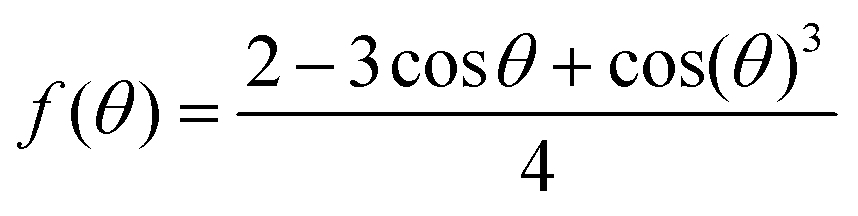
3.2 Thermodynamics and kinetics of nucleation and growth
Thermal energy is usually applied for the conversion of the amorphous into crystalline film in a process affected by both thermodynamic and kinetics factors. RTA makes this transformation possible in a single nucleation-and-growth step similar to that observed in the crystallization of glasses. The crystallization driving force is proportional to the difference between the free energies of the two material states:| ΔG = Gcryst − Gam | (1) |
 | (2) |
 | (3) |
 | (4) |
ln[−ln(1 − Xa)]T = n![[thin space (1/6-em)]](https://www.rsc.org/images/entities/char_2009.gif) lnk + nlnt lnk + nlnt | (5) |
| n = a + bm | (6) |
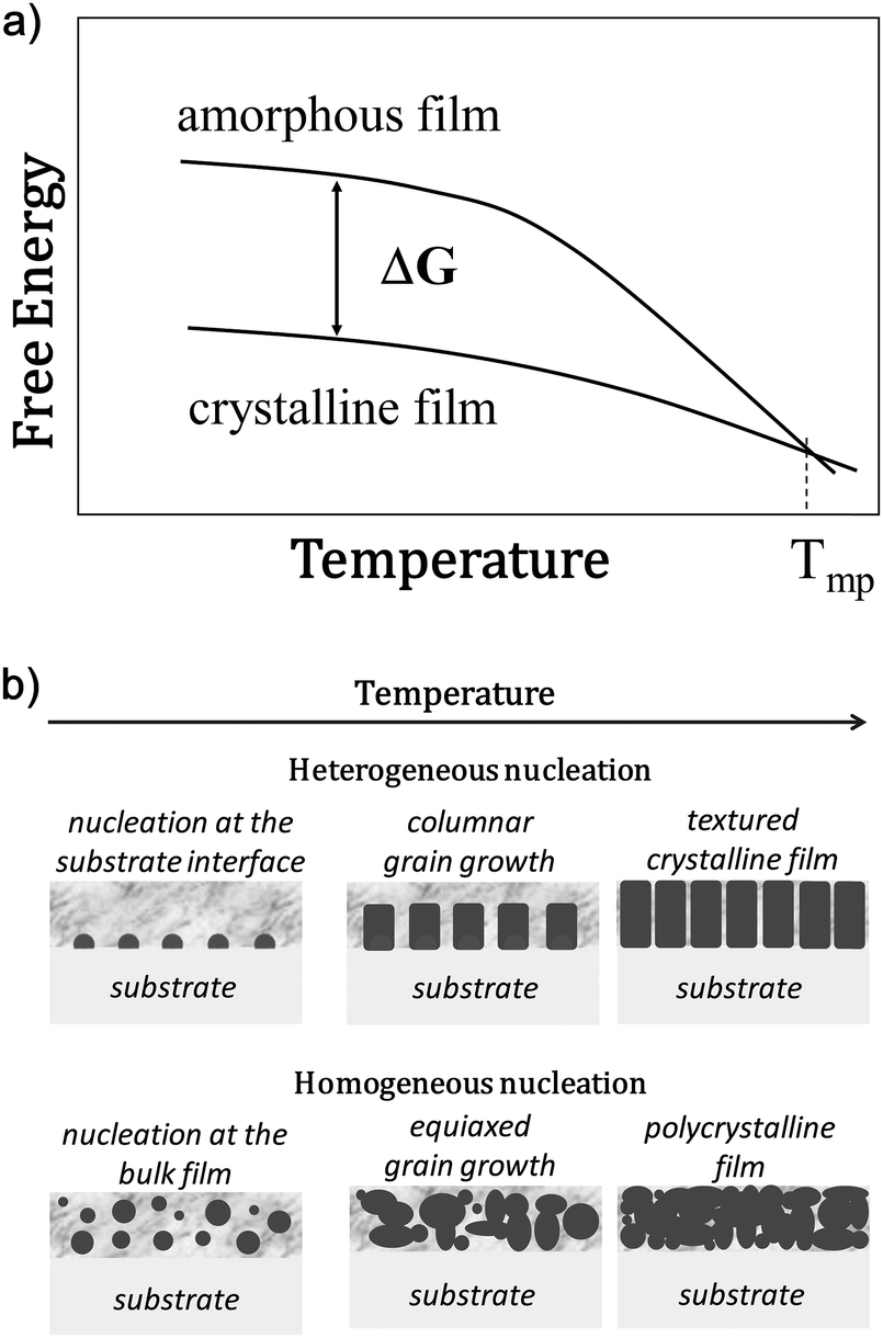 | ||
| Fig. 4 (a) Schematic diagram of the free energies of a solution derived amorphous film and the crystalline perovskite phase (ΔG = driving force for crystallization, Tmp = melting point). (b) Homogeneous and heterogeneous nucleation and growth with temperature for solution derived thin films. | ||
3.3 Low-temperature processing
In 1963, the invention of a complementary metal–oxide–semiconductor (CMOS) circuit configuration established the standard fabrication process followed by the semiconductor industry for manufacturing of integrated circuits. These components are fabricated on silicon wafers through several processing steps, between 20 and 200 depending on the device complexity, resulting in the final thin film transistor. The potential introduction of any new material into microelectronic devices entails thus the use of integration routines fully compatible with the current CMOS process technology.24 Specifically, the fabrication step required to activate the transistor's source/drain after the implantation of dopants sets the upper temperature limit recommended for the whole process. This value is strongly dependent on the CMOS technology node (a concept related to the transistor gate length), which its evolution towards lower values has made possible semiconductor scaling over the last five decades (Moore's law). While thermal budgets for dopant implantation at 850–900 °C were used in 1992 (500 nm node), the transition to sub-100 nm devices from 2004 (90 nm node) and the introduction of nickel silicide for electrical contacts (65 nm node) has further reduced this temperature limit to 450–500 °C at present (according to International Technology Roadmap for Semiconductors). The fact that most metal oxides require a crystalline structure to reach the full potential of their physical properties, and that such crystalline structure is usually attained only at high temperatures (>600 °C), makes the crystallization process the limiting step in the low-temperature processing of these materials (see Fig. 2). This has led to the exploration of novel crystallization pathways rather distant from their conventional synthesis, a sort of paradigm shift introduced in the field not long ago.2–5Over the past decade, we have witnessed a renewed interest in the low-temperature processing of metal oxide thin films that can be attributed to the latest developments of flexible electronics.6 Similar to the fabrication of conventional wafer-based electronics (integrated circuits), the direct integration of metal oxide layers with flexible systems proceeds via deposition and growth onto the substrate. As stated in the Introduction, commercial substrates based on polyimide compounds, like Kapton® or Upilex®, are the ones that withstand the maximum deposition temperature nowadays (around 350 °C). Therefore, the integration of functional metal oxide thin films on flexible plastic is challenging, requiring a substantial reduction of their conventional processing temperatures. Inorganic semiconductors are practically the only metal oxide materials employed today in flexible electronic devices. The reason behind this lies in a particular behavior unique to semiconductor oxides: they display acceptable values of electron mobility—the main physical property that accounts for their electronic functionality—even at the amorphous state (values between 1–10 cm2 s−1 V−1).8 The explanation of this effect is related to the conduction band of post-transition metal oxide semiconductors. This band is composed of spatially spread metal ns orbitals with isotropic shape, where overlapping with neighboring metal ns orbitals is not significantly affected by the distortion of the metal–oxygen–metal chemical bonds derived from the amorphous state. On the contrary, the electron mobility of well-studied covalent semiconductors such as silicon results severely degraded in the amorphous state due to the strongly directive sp3 orbitals, which are very sensitive to structural distortion. This means that semiconductor oxides can be prepared on flexible substrates even at temperatures below 350 °C, despite the disordered structure being obtained in the material. The formation of a defect-free, highly densified metal–oxygen network in the films is the main constraint to afford the high performance of these amorphous materials in electronic devices.
In the following sections, a brief description of the most relevant strategies adopted to induce the crystallization of metal oxide thin films at low temperatures is presented. The strategies fall into two distinctive categories, depending on whether the key process is designed to advance to an early stage either the formation of the amorphous metal–oxygen network (Section 3.3.1) or the direct crystallization of the oxide phase from the former state (Section 3.3.2). Both situations account for the lower temperature finally required to obtain crystalline metal oxide thin films with potential application in electronic devices.
In the first case, different approaches are included that may involve the careful choice of solution chemicals or the synthesis of structurally designed molecular compounds. An example of the former is the introduction of catalysts in solution that accelerate the condensation reactions by consuming hydroxide anions (OH−), which promotes the early formation of the metal–oxygen network in the film.25 Also, amorphous metal oxide thin films have been prepared at low temperature by making use of the localized energy generated in the system during the reaction between acetylacetone or urea, and a metal nitrate, incorporated as chemicals to the precursor solution.26 According to these authors, the reagents may work as fuels and oxidizers, respectively, in such a way that the external application of a low-temperature heating would be able of initiating a highly exothermic redox-based combustion in the as-deposited layer converting the metal precursors into the corresponding metal oxide. Amorphous Zn0.3Sn0.7O1.7 films fabricated at 250 °C by this method showed similar physical properties (electron mobility of ∼1.7 cm2 s−1 V−1) as those of analogous films prepared by conventional synthesis at 400 °C.26 A more sophisticated strategy concerns the synthesis of homo- and hetero-metallic molecular complexes as optimum precursors for metal oxides basing on a close relationship between the molecular structure of the former and the crystal structure of the latter. Besides, these molecular precursors increase the chemical homogeneity of the solution system.27 A good example is that of solutions where polynuclear bismuth oxido clusters are synthesized.28 The molecular structure of this metal precursor resembles that of the β-Bi2O3 phase, which promotes the early-stage formation of a condensed, highly densified amorphous metal–oxygen network (i.e. the prelude to crystallization).
For reducing the temperature of formation of amorphous metal oxide films, the second group of approaches combines rapid thermal treatments with specific processing aids (chemical assisted annealings). Thus, a vertical diffusion technique (VDT) was employed for the fabrication at 280 °C of uniform and dense In–Ga–Zn–O films with values of electron mobility adequate for their use in transistor devices (∼1.3 cm2 s−1 V−1).29 This method enables the formation of the amorphous oxide by an enhanced diffusion of atoms between two consecutively deposited gel layers of the binary (Ga–O) and ternary (In–Zn–O) oxide systems. Rapid post-annealing of this stack promotes the vertical diffusion of the atoms of each layer, yielding a quaternary oxide film (In–Ga–Zn–O) with high performance. Heating processes of solution derived films using different firing atmospheres have also demonstrated to affect the formation of the corresponding amorphous metal–oxygen network. In this way, the sol–gel on chip process30 is based on the enhancement of the metal oxide formation through the hydrolysis and partial condensation of the as-deposited layer on a hot-plate under a controlled atmosphere of water vapor. Further heating below 230 °C led to amorphous semiconductor M1XM2YOZ films (M1 and M2 are metals such as In, Ga, Sn or Zn) with competitive values of electron mobility for applications (∼10 cm2 s−1 V−1). A strong oxidizing environment formed by ozone and active atomic oxygen can also be generated under the UV irradiation of an oxygen atmosphere. The heating at 400 °C of Ta2O5 layers under this environment led to films with optimum properties for using in charge storage memory devices.31 This is because organic residuals are quickly removed from the film by the ozone, and the atomic oxygen reacts with suboxides, improving the film stoichiometry and decreasing the density of charged defects (e.g. oxygen vacancies). Additionally, an increase of the bulk density of sol–gel films under UV irradiation has also been demonstrated for amorphous In–Ga–Zn–O films. The high-energy UV photons induce the photochemical cleavage of the reagents. This facilitates the condensation reactions and the densification of the amorphous film at a low temperature. Adequate values of electron mobility (∼3.8 cm2 s−1 V−1) were measured in these films photo-annealed at ∼150 °C, as a proof of their quality.32
 | ||
| Fig. 5 Schematic illustrations of the nucleation and growth phenomena in metal oxide thin films assisted by the seeding effect, via (a) a seeding layer previously grown on the substrate and (b) crystalline nanoseeds previously introduced within the bulk film. | ||
Another key for lowering the crystallization temperature of metal oxides is based on increasing the mobility of the atoms during the annealing process. The use of a metal (oxide) flux in the synthesis of intermetallic compounds and bulk ceramics is a well-established method in solid state chemistry explicitly designed for that purpose. Here, a metal or a metal oxide that melts at reasonably low temperatures is added to the precursor material, acting thus as a solvent that facilitates the crystallization of high temperature phases by an enhanced diffusion of elements. Due to their relatively low melting points, post-transition metals (usually Ga, In, Tl, Sn, Pb, and Bi) have extensively been used to produce metallic fluxes for the preparation of a wide variety of inorganic materials. A similar effect to the traditional flux synthetic method has been observed in metal oxide thin films as corroborated by many experimental studies. Thus, the addition of excess lead (up to 50 mol%) and bismuth (20 mol%) to precursor solutions of Pb(Zr0.53Ti0.47)O3 and Bi4Ti3O12, respectively, has made possible the crystallization of the corresponding perovskite films at lower temperatures (450–500 °C) than conventional ones.35,36 The reason behind the enhanced crystallization of these films upon metal excess addition remains, however, unclear. Some authors point out that the metal oxide excess may effectively act as a flux for crystal growth, but also as a network modifier facilitating the long-range rearrangement of ions (increase in atomic mobility within the amorphous phase) necessary for crystallization.37 Anyway, the amount of crystallized perovskite phase at a given annealing temperature increases significantly with the percentage of such excess addition.35 Most probably this effect is also present in other compounds, but it has not been systematically studied in metal oxide semiconductors (e.g. Zn–Sn–O, In–Zn–O, In–Ga–Zn–O systems) where the electrical properties of the films are observed to be strongly influenced by the content of certain post-transition metals.38 Finally, irradiation-assisted methods comprising different wavelengths and modes are also considered key strategies to promote the crystallization of metal oxide films at relatively low temperatures. Microwave annealing has shown a great potential for the synthesis of inorganic materials such as nanoparticles, nanostructures, and thin films.2 Since the energy of a microwave photon (2.45 GHz) is rather low to induce chemical reactions, the energy is directly transferred to the material in the form of dielectric heating. This results in a selective and uniform heating within the material, showing lower annealing temperatures and times compared to conventional processes. For example, solution-derived Pb(Zr0.52Ti0.48)O3 thin films pyrolyzed at 400 °C were fully crystallized into the perovskite phase by microwave annealing at 450 °C for 30 min.39 The films were denser and exhibited superior electrical performance (in terms of dielectric and ferroelectric properties) when compared to samples crystallized by conventional heating at 700 °C. Pulsed laser annealing is another irradiation-assisted crystallization technique that employs excimer lasers, usually of ArF (193 nm) and KrF (248 nm), with pulse lengths of several tens of nanoseconds scanning the surface of films.4 Crystallization proceeds via photothermal effect (i.e. generation of thermal energy by photoexcitation) allowing the growth of both epitaxial and polycrystalline thin films. Thus, LaMnO3 thin films4 were epitaxially grown on SrTiO3 substrates at 500 °C and polycrystalline Ba0.7Sr0.3TiO3 perovskite films40 were also obtained at 450 °C by this method. The modeling of the temperatures achieved by pulsed laser irradiation at different thickness of the films reveals a variation from ∼1500 °C at the surface to ∼400 °C at the film/substrate interface. The small diameter of the laser spot (in the range of 2–8 mm), however, restricts the application of this technique to large-area devices.
4. Photochemistry to induce crystallization at low temperatures
During the last decade, crystalline metal oxide films have been obtained at low temperatures exploiting the structural changes induced by UV light in solution derived layers.41 Photochemical reactions are produced in these systems by the absorption of light with energy equal or higher than that of labile chemical bonds of the molecular species present in the precursor. This can lead to chemical bond cleavage and complementary photoreactions, with the subsequent structural evolution and crystallization of the material. In the following sections we summarize the latest and most relevant solution methods that use photochemistry for inducing the low temperature crystallization of metal oxide thin films.4.1 UV light and solution chemistry
Penetration of UV light is limited to the surface region of condensed matter, typically below 200 nm. Therefore, UV irradiation is very effective for inducing chemical changes in thin film materials.41 The illumination of amorphous films with UV light (either with pulsed lasers or continuous irradiation lamps) can produce the thermal or electronic excitation of the system, as shown in Fig. 6.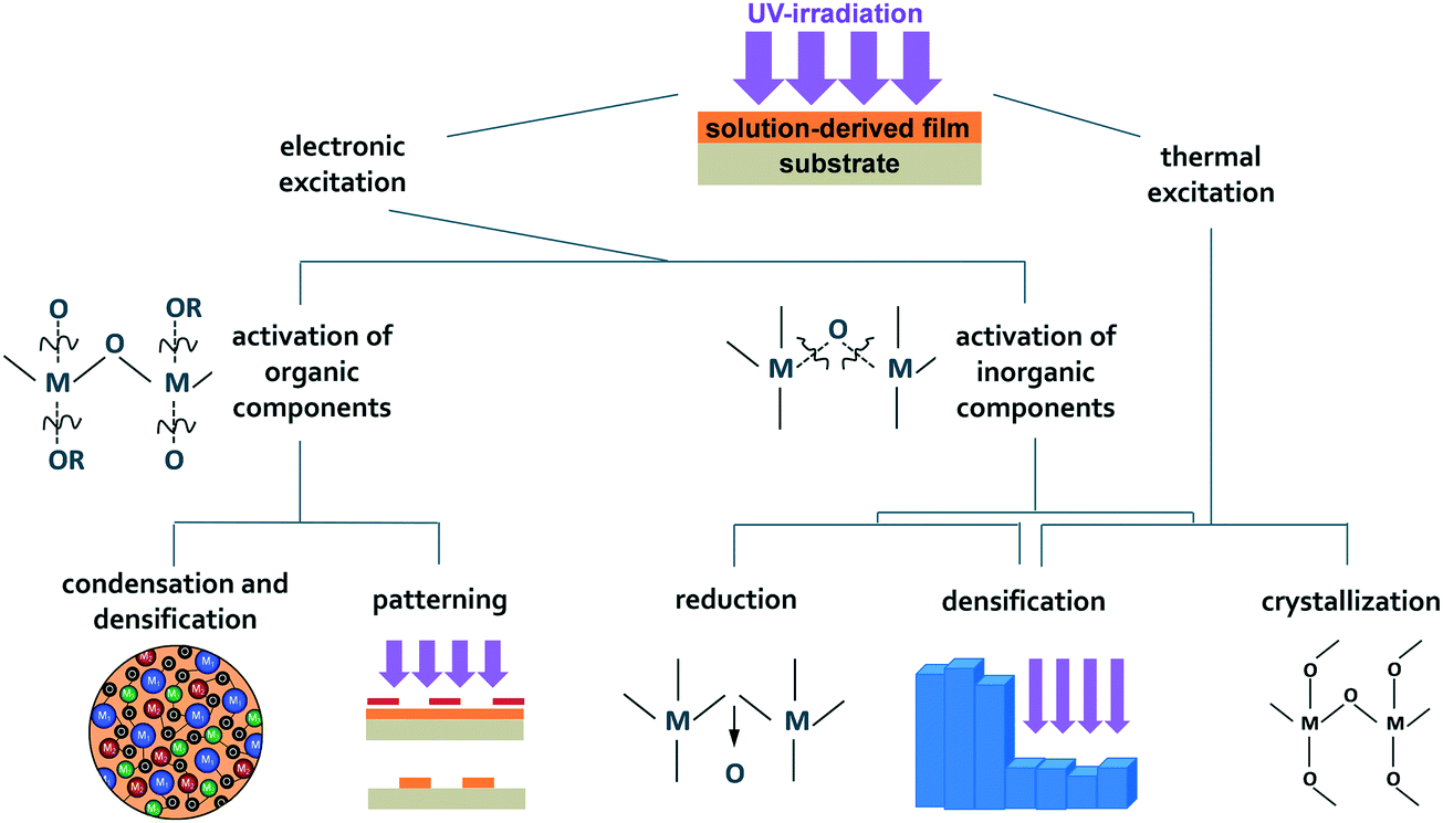 | ||
| Fig. 6 Fundamental effects induced by UV light in solution derived thin films. | ||
For pulsed laser irradiation, the optimum state of the film is a defect-free, highly densified amorphous oxide. Here, irradiation results in a photothermal effect because of the relatively high absorbance of metal oxides in the UV range, the high power provided by pulsed lasers (106–107 W cm−2) and the small area irradiated by the high intensity source. This can lead to local temperatures over thousand degrees Celsius at the surface of the film, which may produce the crystallization of the oxide without applying an external heating.4
On the other hand, precursor solutions used for the deposition of metal oxide thin films are excellent systems for inducing chemical reactions in them by light since they are usually formed by photosensitive compounds (e.g. alkoxides, β-diketonates, etc.). Unlike with pulsed UV lasers, electronic excitation prevails when solution derived films containing UV-absorbing compounds are irradiated with continuous UV lamps. These have much lower power than lasers (10−2–10−1 W cm−2) and can irradiate over large areas under controlled atmospheres, enhancing photochemical reactions and minimizing thermal excitation. Nowadays, high-efficiency excimer lamps from the near (354 nm) to the deep (126 nm) UV region are commercialized to this aim. The range of these excimer wavelengths is shown in Fig. 7, compared with the chemical bond energies of typical functional groups.42 Thus, energetic photons coming from these UV lamps can excite and hence dissociate many types of molecules, generate active chemical species, and ultimately modify the molecular network of the gel layer. This allows pushing the chemical environment far from equilibrium by producing selective reactions and species that are not attainable by conventional thermal processes. Fig. 8 shows some key reactions produced under continuous UV irradiation of solution derived films in an oxygen atmosphere, where several processes may occur. First, irradiation can lead to the bond cleavage of photosensitive organic compounds and metal precursors (i.e. photolysis); formation of reactive species such as strong oxidants like ozone (O3) or atomic oxygen (O(1D)); and reaction among the products and byproducts originated by UV irradiation. Afterwards, metals and oxygen start to bond forming an amorphous metal–oxygen network that becomes denser as condensation proceeds further. The progress of these reactions may result in the formation of the first crystal nuclei in the film. Other compounds like atomic oxygen can react with suboxides or oxygen vacancies ( ) improving the metal oxide stoichiometry and decreasing the density of crystal defects in the film by compensation. In this environment crystallization can finally be accelerated by the reactive species present in the chemical system, such as ˙OH or ˙H radicals. Both reactivity and crystal nucleation efficiency can be controlled not only by the selection of the optimum UV light and irradiation conditions, but also by the appropriate design of photosensitive precursor solutions.
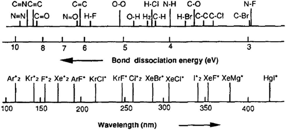 | ||
| Fig. 7 Wavelengths available with excimer sources, compared with a selection of bond-strengths of common molecules. Reprinted with permission from ref. 42. Copyright 1997 Elsevier Science B.V. | ||
 | ||
| Fig. 8 Key processes occurring during the continuous UV light irradiation in oxygen of metal oxide films prepared by chemical solution deposition. Examples of some potential reactions are shown. | ||
4.2 Molecular design of photosensitive precursors
Transition and post-transition metals can react with some organic compounds forming photosensitive coordination complexes, where electronic transitions may induce intra- and inter-molecular processes after light absorption. Excited states associated with the bands of a metal centered (MC) ligand transition, ligand to metal charge transfer (LMCT), metal to ligand charge transfer (MLCT) and intraligand centered (LC) transitions can be generated by the UV irradiation of these complexes.43Few examples are found in the literature using this type of photosensitive molecular precursors to attain crystalline metal oxide films at low temperatures. This is the case of β-diketonate metal complexes with absorption bands in the UV-range due to LC transitions involving π → π* orbitals. The electronic excitation of these compounds upon irradiation results in the dissociation of the chelate bonds, which promotes the metal oxide crystallization. Thus, ferroelectric PbTiO3 and Pb(Zr1−xTix)O3 perovskite thin films have been obtained from solutions containing titanium and zirconium alkoxides modified with acetylacetonate groups. These are photosensitive solutions (Fig. 9a) where a prompt elimination of the organic compounds is produced after UV irradiation of the films deposited from the corresponding precursors (Fig. 9b). This advances the crystallization of the perovskite phase at the low temperature of 450 °C (Fig. 9c), leading in addition to ferroelectric films with properties of interest for electronic devices.24
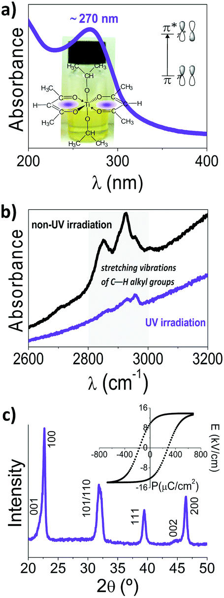 | ||
| Fig. 9 (a) UV spectrum of a precursor solution of (Pb,Ca)TiO3 containing titanium bis-acetylacetonate di-isoproxide, showing the molecular structure of this compound. A picture of the photosensitive solution and a diagram of the corresponding electronic transition are also shown. (b) FTIR spectra of the gel layers deposited from the former solution and treated with and without UV-irradiation at 250 °C. (c) XRD pattern of the photoactivated (Pb,Ca)TiO3 film crystallized at 450 °C. Inset in (c) shows the ferroelectric hysteresis loop of this film. Adapted with permission from ref. 24. Copyright 2004 Wiley-VCH Verlag GmbH & Co. KGaA. | ||
Other compounds like alkanolamines can also react with a large number of metals, where charge transfer excited states result from the transitions between the molecular orbitals of the metallic center and the alkanolamine ligand (MLCT and LMCT).43 These transitions correspond to very intense absorption bands in the ultraviolet region, with molar attenuation coefficients three orders of magnitude higher than the typical values of other light absorbing compounds. Ti(IV), Fe(III), Pb(II) or Bi(III) are elements that have been reported to form photosensitive metal complexes with N-methyldiethanolamine, CH3N(CH2CH2OH)2.28,44,45Fig. 10a shows the molecular structure of this type of metal complex for a Bi(III) precursor. The photosensitivity of the solutions containing this complex is clearly evidenced by its dark brownish color visible to the naked eye, showing an absorption band in the UV region at ∼250 nm.45 The irradiation of the films deposited from this solution produces a quick elimination of the organics (Fig. 10b) accompanied by a progressive crystallization at low temperature (250 °C) of the β-Bi2O3 phase (Fig. 10c). Note that this polymorph is a high-temperature metastable phase (497–667 °C) that results stabilized in these films at room temperature owing to photochemical reactions.28 This type of complexes have also been synthesized in solution as precursors for functional complex oxide thin films (e.g. ferroelectric PbTiO3, piezoelectric (Bi0.5Na0.5)0.945Ba0.055TiO3 or multiferroic BiFeO3), which were crystallized at a temperature as low as 400 °C after irradiation of the deposited layers. A significant improvement in the physical properties of the irradiated films was obtained with respect to the non-irradiated ones, which makes the former adequate for their potential use in electronic devices with different functionalities (e.g., memories, actuators, sensors).45
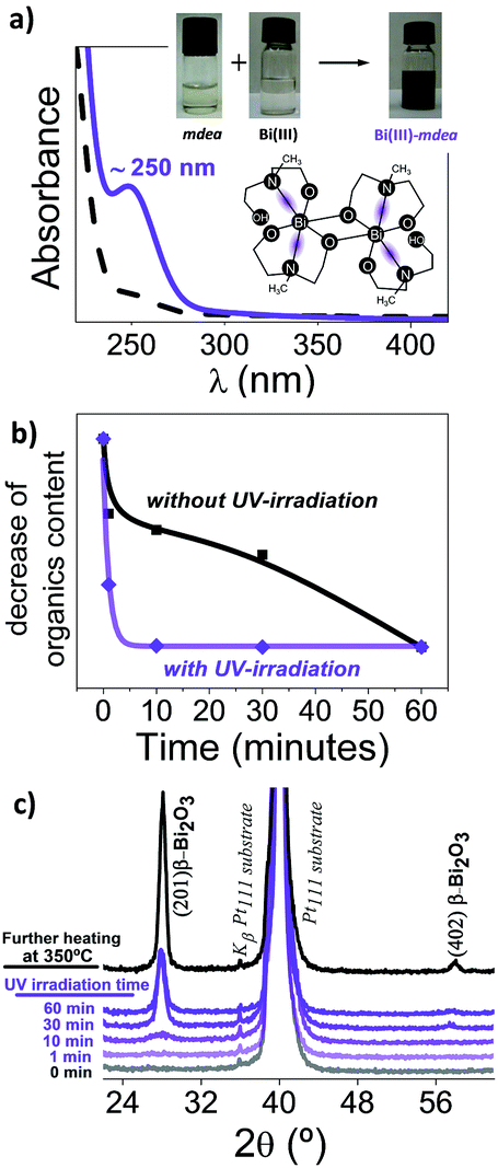 | ||
| Fig. 10 (a) UV spectra of the Bi(III) and Bi(III)-mdea (N-methyldiethanolamine) solutions, showing the molecular structure proposed for the Bi(III)-mdea complex. Pictures of the mdea reagent, the Bi(III) solution and the resulting Bi(III)-mdea one after synthesis are also shown. (b) Decrease of the organics content (calculated from the ν(C–H) bands of the corresponding FTIR spectra) in the films deposited from the Bi(III)-mdea solution as a function of the irradiation time. (c) XRD patterns of the β-Bi2O3 thin films prepared from the former solution under UV-irradiation at 250 °C for different times, and after further annealing at 350 °C. Adapted with permission from ref. 45. Copyright 2014 The Royal Society of Chemistry. | ||
4.3 Ozonolysis and photoactivation
The photolysis of oxygen, O2, produces reactive oxygen species such as O(3P), O(1D) and O(1S). Subsequent processes are the reaction of O(3P) with O2 to produce O3 (ozone) or the photolysis of O3 to form O2 and O(1D) again. The strong oxidant character of the generated O3 atmosphere promotes the chemical bond cleavage by oxidation (ozonolysis) of the organic compounds present in the solution derived film, which promotes the formation of a continuous metal–oxygen network. Besides, UV illumination may lead to a photoactivated chemical system (photoactivation), where reactions take place among the excited species present in the film and those developed in the local atmosphere by irradiation. In this highly reactive medium, atomic oxygen (e.g. O(3P), O(1D) or O(1S)) and other free radicals (e.g. ˙C, ˙OH, ˙CO, ˙NH) are generated, which can promote the crystallization of the metal oxide film by complementary photoreactions (see Fig. 8). Thus, the reduction of the crystallization temperature of metal oxides by ozonolysis and photoactivation is illustrated by the results previously shown in Fig. 10b and c, where the irradiation of UV-absorbing molecular precursors in oxygen leads to the formation of a very reactive environment that facilitates the nucleation of the crystal phase in the film.45By making use of these phenomena, polycrystalline (Pb0.76Ca0.24)TiO3 films have been obtained at 450 °C after the UV-assisted rapid thermal processing in oxygen of layers deposited from photosensitive sol–gel solutions.24 Improvement in the dielectric properties of these films is related to the higher degree of crystallinity obtained after ozonolysis and to the more precise stoichiometry resulted from the formation of reactive species that compensate crystal defects. Another excellent example of how the genesis of a photoactivated chemical system can affect the crystallization of metal oxide films is the use of aqueous citrato-peroxo metal precursors.46 The thermal decomposition of the respective films produces intermediate organic acids, anhydrides, amides, and imides which are strong UV-absorbing species. Besides, highly reactive ˙H, ˙NH and ˙NH2 radicals are formed by the photolysis of water and ammonia during irradiation. All this leads to a very active chemical system by UV illumination under an optimum temperature window, which is exploited for the low temperature crystallization (400 °C) of perovskite PbTiO3 films with an appropriate ferroelectric response.
Finally, it is also worth noting the role of the photoactivation in the crystallization process observed for other materials. An accelerated crystallization of aluminosilicate minerals (zeolites) via hydroxyl radicals has been achieved with UV irradiation at room temperature of SiO2/0.46Al2O3/4.4Na2O/60H2O solutions under hydrothermal conditions. The illumination with high irradiances increases the concentration of the ˙OH radicals generated by UV light, which speeds up the nucleation stage of the zeolite crystals.47
4.4 Photocatalysis-assisted decomposition
The term photocatalysis includes a wide variety of secondary reactions (e.g. oxidation, reduction, condensation, etc.) promoted by the photon-induced electron–hole pair generated in a photocatalytic material that can lead to the effective decomposition of organic matter adsorbed on its surface. Particularly, heterogeneous photocatalysis has made possible the development of self-cleaning windows through the action of a thin transparent layer of TiO2 (the semiconductor photocatalyst par excellence) deposited on the glass window: organic dirt is chemically broken down by sunlight photocatalysis and washed afterwards away with rainwater.48 Today, more than 200 species can be decomposed by TiO2 photocatalysis in aqueous media for wastewater purification, including organic compounds such as alkanes, aliphatic alcohols and carboxylic acids among many other classes (e.g. aromatics, polymers, dyes and surfactants).Recently, we have demonstrated that the photodegradation of organic pollutants typically induced by TiO2 photocatalysis could be extrapolated to promote the decomposition of the organic moieties of the metal precursors employed in chemical solution deposition.3 The proposed mechanism is depicted in Fig. 11a, where precursor solutions of ferroelectric Pb(Zr0.3Ti0.7)O3 and multiferroic BiFeO3 complex oxides were subjected to photocatalysis by TiO2 nanoparticles dispersed in the liquid medium. Upon light absorption, oxidation of the organic groups (hydrocarbons, alcohols, carboxylates, ketones) present in the metal precursors proceeds via photogenerated holes and electrons, the last ones contributing to the formation of strong oxidizing radicals such as ˙OH. Experimental results confirmed the modification of the molecular structure of the solution, where the partial decomposition of metal precursors and their subsequent polycondensation was observed. Most important, the photocatalytic effects induced by TiO2 nanoparticles when irradiated were carried out by an advanced oxidation process solely at room temperature.
 | ||
| Fig. 11 (a) Schematic representation of the photocatalysis-assisted decomposition process. (b) Decomposition temperatures of PbZr0.3Ti0.7O3 (PZT) and BiFeO3 (BFO) precursors as a function of the photocatalysis time. (c) X-ray patterns of PbZr0.3Ti0.7O3 (PZT) and BiFeO3 (BFO) thin films annealed at low temperatures from their respective initial and photocatalyzed precursor solutions. Adapted with permission from ref. 3. Copyright 2015 Wiley-VCH Verlag GmbH & Co. KGaA. | ||
Once the TiO2 nanoparticles are removed from the solution after the photocatalytic process, a so-called “low-temperature liquid precursor” is obtained. Such precursor requires a lower energy input (via thermal treatment) for the crystallization of the corresponding metal oxide with respect to the initial (non-photocatalyzed) solution. This is reflected in the decomposition temperature of both Pb(Zr0.3Ti0.7)O3 and BiFeO3 precursors, which significantly decreases after an optimum photocatalytic reaction time (Fig. 11b). The molecular structure of the precursor at this stage results in a metal–oxygen network with an improved degree of condensation prior to crystallization. The energy for the formation of the perovskite oxide is thus reduced, and crystalline thin films are obtained at lower temperatures with respect to the initial precursor. Fig. 11c shows a comparative of the X-ray patterns of metal oxide thin films processed at 350 °C (Pb(Zr0.3Ti0.7)O3) and 325 °C (BiFO3) with and without photocatalysis. Whereas amorphous films are obtained from the initial solutions, reflections corresponding to the perovskite phase are detected in the X-ray patterns of the films derived from the photocatalyzed solutions. This demonstrates the efficiency of this method for the crystallization of metal oxides thin films at low temperatures. The proposed concept, which merges two distant disciplines in materials science such as the hererogeneous photocatalysis and the low-temperature processing of functional films, is foreseen to be applicable to many other metal oxides.
5. Crystalline metal oxide thin films in flexible devices
Thin films of metal oxides can be at the core of next-generation flexible electronic systems provided their integration with a facile, low-cost technology is accomplished. Although transfer printing methods have been used successfully, they require multiple steps that increase the complexity (and hence the costs) of the process and eventually frustrate their widespread application. The alternative methods shown in this review enable the direct growth of metal oxide layers on flexible substrates, opening new and promising horizons in this field. Particularly, the recent incorporation of crystalline oxides to these systems provides a wide range of novel functionalities beyond the capabilities of current flexible electronic devices. As a result, metal oxides are readily available for the development of disruptive applications in macroelectronics, digital information and communication technologies or wearable systems, being especially important for tackling societal challenges as healthcare. A selection of the most representative applications that can benefit from the use of low-temperature crystallized metal oxide films is given in this section.Transparent films with self-cleaning properties could significantly extend the applications of new smart windows comprised of flexible devices (e.g. electrochromic layers). In a recent work, we have carried out the realization of photocatalytic Bi2O3 thin films on a flexible polyimide (PI) substrate at 250–350 °C using a photochemical solution process.28 The crystallization of the metastable (high-temperature) β-Bi2O3 polymorph is responsible for the excellent photocatalytic activity under visible light of these flexible films with potential applications in self-cleaning surfaces, photocatalytic reactors or wearable antimicrobial fabrics.
New lighting devices can be fabricated from metavanadate phosphor films after their direct integration onto flexible organic substrates. By using an excimer-lamp-assisted metal–organic deposition process, crystalline RbVO3 thin films have been prepared on polyethylene terephthalate (PET) substrates close to room temperature.4 These compounds are characterized by the presence of absorption bands in the ultraviolet region and broad-band emissions in the visible part. Consequently, bright white emission is observed in the RbVO3 thin films on PET upon ultraviolet illumination, while no photoluminescence is noticed under ambient light. The introduction of additional layers of other phosphor materials on the device results in the possibility of color modification for the luminescence of these films.
Flexible non-volatile memories are crucial components of future smart cards and labels, RFID tags (radio-frequency identification) or bendable mobile devices (smartphones, tablets, laptops). Thin films of metal oxides provide two distinct states of material resistance (resistor-based memory), capacitance (capacitor-based memory) or polarization (transistor-based memory) required for the storage information in the binary code. Active layers of transition metal oxides (e.g. TiO2, nanoporous WO3−x) have been prepared by low-temperature processes on PET or poly(ether sulfone) (PES) substrates for new flexible resistive random access memory (RRAM) devices.49Fig. 12a shows the memory switching characteristics of such type of flexible devices, where the initial high-resistance state is changed to a low-resistance one upon the application of an external voltage. This behavior is reversible, and reliable operation is obtained under bending conditions (radius of curvature of ∼5.53 mm).
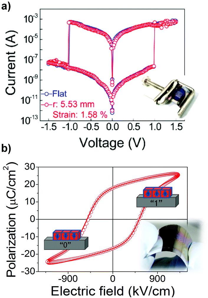 | ||
| Fig. 12 (a) Resistive switching characteristics of a flexible nanoporous WO3−x thin film showing the two resistance states with potential use for memory devices (inset shows a photograph of the flexible sample). Reprinted with permission from ref. 49. Copyright 2016 American Chemical Society. (b) Ferroelectric hysteresis loop of a flexible PbZr0.3Ti0.7O3 thin film denoting the two distinct polarization states that allows binary memory storage (inset shows a photograph of the flexible sample). Adapted with permission from ref. 5. Copyright 2014 Wiley-VCH Verlag GmbH & Co. KGaA. | ||
Crystalline Pb(Zr0.3Ti0.7)O3 ferroelectric thin films have also been prepared on flexible PI substrates at temperatures between 300–350 °C giving rise to new flexible ferroelectric random access memories (FeRAMs). We have demonstrated that this is feasible using a strategy that combines the photochemical solution deposition of seeded diphasic sol–gel precursors.5 The ferroelectric hysteresis loop of these films is depicted in Fig. 12b, where the positive (upward) and negative (downward) remanent polarizations are defined as the respective “1” and “0” states of the memory. The values of remanent polarization obtained from this loop meet the switching charge density demanded today for this type of memory. In summary, integration of these crystalline metal oxides on plastic foils would pave the way for inexpensive, lightweight, and foldable memory devices directed towards future high-tech products.
Flexible sensors are required for a wide range of biomedical applications where the rigid counterparts present some technical limitations. For example, thermal sensors integrated on flexible polymer substrates may provide significant benefits for monitoring body temperature with respect to traditional methods using sophisticated infrared digital cameras or punctual temperature detectors. Crystalline thin film thermistors of Mn1.56Co0.96Ni0.48O4 have been prepared for this purpose on flexible PET substrates at room temperature by means of laser irradiation.50 The resulting devices show strong variations on their electrical resistance with small changes in temperature, particularly a negative-temperature-coefficient (NTC) behavior, which confirms their suitability for flexible sensors in skin thermography applications. Particularly, when evaluating the temperature sensing properties in a finger approach test, the response of the metal oxide thin film thermistor results much faster and more precise compared to that given by a commercial rigid ceramic chip thermistor.
Ferroelectric oxides are also excellent candidates for flexible sensors (and actuators) due to their pyro- and piezoelectric properties. Recently, we have developed a low-temperature solution method (i.e. a photocatalytically assisted decomposition process) for the preparation of ferroelectric Pb(Zr0.3Ti0.7)O3 and multiferroic BiFeO3 perovskite thin films at temperatures compatible with flexible PI substrates (Fig. 13a).3Fig. 13b shows the topography of a 325 °C-annealed BiFeO3 thin film where inversion ferroelectric domains (180°) can be also observed by piezoresponse force microscopy (PFM) (Fig. 13c). The functionality of the flexible BiFeO3 film is not compromised due to the low temperature crystallization, and polarization switching is achieved, as the local piezoelectric hysteresis loop shown in Fig. 13d demonstrates. This reveals its potential application in tactile sensors or self-powering devices (based on piezoelectric energy harvesting) for electronic skin or wearable systems.
 | ||
| Fig. 13 (a) Photograph of a flexible BiFeO3 thin film. (b) Topography and (c) out of plane PFM phase images of the surface of a 325 °C-annealed BiFeO3 thin film. (d) Local piezoelectric hyteresis loop measured on the flexible film. Adapted with permission from ref. 3. Copyright 2015 Wiley-VCH Verlag GmbH & Co. KGaA. | ||
6. Conclusions and outlook
The versatility of wet chemical methods allows the easy exploration of novel crystallization pathways for metal oxides thin films and makes them fundamental in the search of low-temperature methods. The strategies shown in this review focus either on promoting the formation of a defect-free, highly densified metal–oxygen network (e.g. design of the solution chemistry, chemical assisted annealings) or on aiding the subsequent crystallization of the metal oxide phase (e.g. seeding effect, flux synthesis or microwave/laser annealing). While both approaches are effective with regard to the low-temperature-induced crystallization of metal oxides thin films, their synergistic combination is expected to bring further fascinating advances to this field.The prospect of using light as an alternative source of energy to induce crystallization by photochemistry has significantly contributed to decreasing the processing temperatures of metal oxide thin films at the bare minimum today. Complex oxide films with processing temperatures traditionally over 600 °C can be crystallized now below 350 °C, a temperature range considered practically unfeasible several decades ago. While the lower temperature limit achievable for these materials remains uncertain, there is no doubt that it will be linked to the nucleation and growth processes that ultimately define their performance. Thus, low-temperature solution methods show unique features for the reliable integration of crystalline metal oxides into flexible and cost-effective electronics over large areas. Translating this technology to the industry still requires some obstacles to be overcome, such as the implementation of certain processes (e.g. irradiation systems) into the manufacturing routine. The reduction of the energy consumption upon decreasing the processing temperature may bring closer the transition towards a sustainable manufacturing system with practically null heating demands. Up to now, there is no limiting temperature reported below which crystallization of metal oxide thin films is not possible. This makes the room-temperature crystallization the most challenging development envisioned for this field. For surpassing the thermally-activated barriers required for diffusion, the formation of an ideal metal–oxygen inorganic network with an arrangement of atoms practically equal to the structure of the crystalline phase may become the road to success.
Conflicts of interest
There are no conflicts to declare.Acknowledgements
The authors acknowledge funding from Spanish Project MAT2016-76851-R (MINECO). I. B. acknowledges financial support by Fundación General CSIC (ComFuturo Programme). We are grateful to Dr R. Sirera at Universidad de Navarra (Spain) for his valuable contribution to part of the work presented in this review.References
- T. G. Gutowski, M. S. Branham, J. B. Dahmus, A. J. Jones and A. Thiriez, Environ. Sci. Technol., 2009, 43, 1584–1590 CrossRef CAS PubMed.
- S. Diodati, P. Dolcet, M. Casarin and S. Gross, Chem. Rev., 2015, 115, 11449–11502 CrossRef CAS PubMed.
- I. Bretos, R. Jiménez, D. Pérez-Mezcua, N. Salazar, J. Ricote and M. L. Calzada, Adv. Mater., 2015, 27, 2608–2613 CrossRef CAS PubMed.
- T. Nakajima, K. Shinoda and T. Tsuchiya, Chem. Soc. Rev., 2014, 43, 2027–2041 RSC.
- I. Bretos, R. Jiménez, A. Wu, A. I. Kingon, P. M. Vilarinho and M. L. Calzada, Adv. Mater., 2014, 26, 1405–1409 CrossRef CAS PubMed.
- Special Issue: Flexible and Stretchable Devices, Adv. Mater., 2016, 28, 4165–4562 CrossRef.
- E. Dagotto, Science, 2005, 309, 257–262 CrossRef CAS PubMed.
- K. Nomura, H. Ohta, A. Takagi, T. Kamiya, M. Hirano and H. Hosono, Nature, 2004, 432, 488–492 CrossRef CAS PubMed.
- J. Guo, H. Guo, A. L. Baker, M. T. Lanagan, E. R. Kupp, G. L. Messing and C. A. Randall, Angew. Chem., Int. Ed., 2016, 55, 11457–11461 CrossRef CAS PubMed.
- R. I. Walton, Chem. Soc. Rev., 2002, 31, 230–238 RSC.
- K. L. Choy, Prog. Mater. Sci., 2003, 48, 57–170 CrossRef CAS.
- D. Mariotti, T. Belmonte, J. Benedikt, T. Velusamy, G. Jain and V. Svrcek, Plasma Processes Polym., 2016, 13, 70–90 CrossRef CAS.
- C. Sanchez, L. Rozes, F. Ribot, C. Laberty-Robert, D. Grosso, C. Sassoye, C. Boissiere and L. Nicole, C. R. Chim., 2010, 13, 3–39 CrossRef CAS.
- C. J. Brinker and G. W. Scherer, Sol–Gel Science: The Physics and Chemistry of Sol–Gel Processing, Academic Press, Boston, MA, 1990 Search PubMed.
- P. H. Mutin and A. Vioux, J. Mater. Chem. A, 2013, 1, 11504–11512 CAS.
- M. L. Calzada, Sol-Gel Electroceramic Thin Films, in The Sol-Gel Handbook: Synthesis, Characterization, and Applications, ed. D. Levy and M. Zayat, Wiley-VCH, Weinheim, 2015, ch. 27, vol. 2, pp. 841–881 Search PubMed.
- R. W. Schwartz, T. Schneller and R. Waser, C. R. Chim., 2004, 7, 433–461 CrossRef CAS.
- S. T. Meyers, J. T. Anderson, C. M. Hung, J. Thompson, J. F. Wager and D. A. Keszler, J. Am. Chem. Soc., 2008, 130, 17603–17609 CrossRef CAS PubMed.
- L. G. Hubert-Pfalzgraf, Coord. Chem. Rev., 1998, 178, 967–997 CrossRef.
- Q. X. Jia, T. M. McCleskey, A. K. Burrell, Y. Lin, G. E. Collis, H. Wang, A. D. Q. Li and S. R. Foltyn, Nat. Mater., 2004, 3, 529–532 CrossRef CAS PubMed.
- V. Nicolosi, M. Chhowalla, M. G. Kanatzidis, M. S. Strano and J. N. Coleman, Science, 2013, 340, 1226419 CrossRef.
- R. W. Schwartz, J. A. Voight, B. A. Tuttle, D. A. Payne, T. L. Reichert and R. S. Dasalla, J. Mater. Res., 1997, 12, 444–456 CrossRef CAS.
- M. Avrami, J. Chem. Phys., 1941, 9, 177–184 CrossRef CAS.
- M. L. Calzada, I. Bretos, R. Jiménez, H. Guillon and L. Pardo, Adv. Mater., 2004, 16, 1620–1624 CrossRef CAS.
- S. Jeong and J. Moon, J. Mater. Chem., 2012, 22, 1243–1250 RSC.
- M.-G. Kim, M. G. Kanatzidis, A. Facchetti and T. J. Marks, Nat. Mater., 2011, 10, 382–388 CrossRef CAS PubMed.
- B. Malic, M. Kosec, I. Arcon and A. Kodre, J. Eur. Ceram. Soc., 2005, 25, 2241–2246 CrossRef CAS.
- D. Pérez-Mezcua, I. Bretos, R. Jiménez, J. Ricote, R. J. Jiménez-Rioboó, C. G. da Silva, D. Chateigner, L. Fuentes-Cobas, R. Sirera and M. L. Calzada, Sci. Rep., 2016, 6, 39561 CrossRef PubMed.
- S. Yoon, S. J. Kim, Y. J. Tak and H. J. Kim, Sci. Rep., 2017, 7, 43216 CrossRef CAS PubMed.
- K. K. Banger, Y. Yamashita, K. Mori, R. L. Peterson, T. Leedham, J. Richard and H. Sirringhaus, Nat. Mater., 2011, 10, 45–50 CrossRef CAS PubMed.
- I. W. Boyd and J.-Y. Zhang, Solid-State Electron., 2001, 45, 1413–1431 CrossRef CAS.
- Y.-H. Kim, J.-S. Heo, T.-H. Kim, S. Park, M.-H. Yoon, J. Kim, M. S. Oh, G.-R. Yi, Y.-Y. Noh and S. K. Park, Nature, 2012, 489, 128–132 CrossRef CAS PubMed.
- C. K. Kwok and S. B. Desu, J. Mater. Res., 1993, 8, 339–344 CrossRef.
- A. Wu, P. M. Vilarinho, I. Reaney and I. M. Miranda-Salvado, Chem. Mater., 2003, 15, 1147–1155 CrossRef CAS.
- H. Suzuki, T. Koizumi, Y. Kondo and S. Kaneko, J. Eur. Ceram. Soc., 1999, 19, 1397–1401 CrossRef CAS.
- K.-H. Xue, J. Celinska and C. A. Paz de Araujo, Appl. Phys. Lett., 2009, 95, 052908 CrossRef.
- A. D. Polli, F. F. Lange and C. G. Levi, J. Am. Ceram. Soc., 2000, 83, 873–881 CrossRef CAS.
- E. Fortunato, P. Barquinha and R. Martins, Adv. Mater., 2012, 24, 2945–2986 CrossRef CAS PubMed.
- A. Bhaskar, H. Y. Chang, T. H. Chang and S. Y. Cheng, Nanotechnology, 2007, 18, 395704 CrossRef PubMed.
- O. Baldus and R. Waser, J. Eur. Ceram. Soc., 2004, 24, 3013–3020 CrossRef CAS.
- H. Imai, Ultraviolet (UV) Irradiation, in Handbook of Sol-gel Science and Technology: Processing, Characterization and Applications, ed. S. Sakka, Kluwer Academic Publishers, Dordrecht, 2005, ch. 27, vol. 1, pp. 639–650 Search PubMed.
- I. W. Boyd and J. Y. Zhang, Nucl. Instrum. Methods Phys. Res., Sect. B, 1997, 121, 349–356 CrossRef CAS.
- P. S. Wagenknecht and P. C. Ford, Coord. Chem. Rev., 2011, 255, 591–616 CrossRef CAS.
- N. Martín-Arbella, I. Bretos, R. Jiménez, M. L. Calzada and R. Sirera, J. Mater. Chem., 2011, 21, 9051–9059 RSC.
- D. Pérez-Mezcua, R. Sirera, R. Jiménez, I. Bretos, C. De Dobbelaere, A. Hardy, M. K. Van Bael and M. L. Calzada, J. Mater. Chem. C, 2014, 2, 8750–8760 RSC.
- C. De Dobbelaere, M. L. Calzada, R. Jimenez, J. Ricote, I. Bretos, J. Mullens, A. Hardy and M. K. Van Bael, J. Am. Chem. Soc., 2011, 133, 12922–12925 CrossRef CAS PubMed.
- G. Feng, P. Cheng, W. Yan, M. Boronat, X. Li, J.-H. Su, J. Wang, Y. Li, A. Corma, R. Xu and J. Yu, Science, 2016, 351, 1188–1191 CrossRef CAS PubMed.
- I. P. Parkin and R. G. Palgrave, J. Mater. Chem., 2005, 15, 1689–1695 RSC.
- Y. Ji, Y. Yang, S.-K. Lee, G. Ruan, T.-W. Kim, H. Fei, S.-H. Lee, D.-Y. Kim, J. Yoon and J. M. Tour, ACS Nano, 2016, 10, 7598–7603 CrossRef CAS PubMed.
- T. Nakajima and T. Tsuchiya, J. Mater. Chem. C, 2015, 3, 3809–3816 RSC.
Footnote |
| † Electronic supplementary information (ESI) available. See DOI: 10.1039/c6cs00917d |
| This journal is © The Royal Society of Chemistry 2018 |