
Three-dimensional titanium oxide nanoarrays for perovskite photovoltaics: surface engineering for cascade charge extraction and beneficial surface passivation†
Wu-Qiang
Wu
 a,
Dehong
Chen
*ab,
Yi-Bing
Cheng
*c and
Rachel A.
Caruso
*ad
a,
Dehong
Chen
*ab,
Yi-Bing
Cheng
*c and
Rachel A.
Caruso
*ad
aParticulate Fluids Processing Centre, School of Chemistry, The University of Melbourne, Melbourne, Victoria 3010, Australia
bResearch School of Chemistry, The Australian National University, Acton 2601, Australia. E-mail: dehong.chen@anu.edu.au
cARC Centre of Excellence in Exciton Science, Department of Materials Science and Engineering, Monash University, Victoria 3800, Australia. E-mail: yibing.cheng@monash.edu
dRMIT University, Melbourne, Victoria 3000, Australia. E-mail: rachel.caruso@rmit.edu.au
First published on 22nd September 2017
Abstract
Improved photovoltaic performance is reported for perovskite solar cells (PSCs) based on three-dimensional (3D) titanium oxide nanoarray electron transporting layers (ETLs). A solution-process is used to fabricate 3D nanoarrays that consist of rutile TiO2 nanorods (RTNR) with optimal lengths of 600 nm and an outside layer made of rutile, anatase or amorphous TiO2 nano-branches (referred to as RTB, ATB and Am-TB, respectively). These nanoarrays benefit perovskite precursor infiltration and increase the interfacial contact between the perovskite layer and ETL for efficient charge extraction. The PSCs based on the RTNR@ATB or RTNR@Am-TB arrays exhibit enhanced performance with improved open-circuit voltage (Voc) and fill factor (FF), compared to the RTNR@RTB or pristine RTNR counterparts. This is assigned primarily to the appropriate band alignment between the nanorods and nano-branches forming a favorable charge extraction ‘energy cascade’, and to a beneficial surface passivation effect limiting charge recombination. PSCs (with minimal hysteresis) achieved 16.06% efficiency when the rutile trunks were modified with surface amorphous nano-branches, with a short-circuit photocurrent density (Jsc) of 21.80 mA cm−2, Voc of 1010 mV and FF of 0.73. This unique morphological design provides an approach for constructing novel 3D electrodes for the fabrication of optoelectronic devices.
Introduction
In recent years, the organic–inorganic halide perovskite solar cells (PSCs) have attracted growing attention owing to their advantages of high device performance, low production cost and simple fabrication process.1–4 Over the last few years, the power conversion efficiencies (PCEs) of PSCs has increased from 3.8% in 2009,5 to a certified record exceeding 22.1% in 2016.6 To date, various highly efficient PSCs have been demonstrated based on planar,2 mesoscopic1 or integrated mesoscopic/planar device architectures.7 In mesostructured PSCs, the electron transport layer (ETL) is responsible for selectively extracting photogenerated electrons from the perovskite light absorber and simultaneously serving as a blocking layer to prohibit direct contact between the conductive substrate/perovskite and the conductive substrate/hole transporting material (HTM).8To improve the performance of PSCs, research has focused on the optimization of ETL morphologies (e.g. 0D nanoparticles, 1D nanowires, 2D nanosheets and 3D hierarchical structures)9–12 and modification of the ETL/perovskite interface.13,14 Typically, the ETL is engineered to be mesoporous in order to provide a large surface area for perovskite contact. 0D mesoporous nanoparticles are representative structures with the merits of high surface-to-volume ratios for larger amounts of perovskite loading. However, intrinsic limitations such as the existence of numerous grain boundaries, defects and surface states within the disordered nanoparticulate networks would hamper the electron transport and increase the probability of charge recombination.15 1D TiO2 nanoarrays (nanorods, nanowires and nanotubes) have been demonstrated to provide a direct pathway for fast electron transport and porous channels for improved perovskite infiltration.16–18 However, the low conductivity and the inherent surface defect states of TiO2 have been regarded as obstacles to obtain efficient charge collection despite the preferred electron pathway along the 1D axis. The injected electrons may recombine with the holes at the interface between the ETL and the perovskite layer, which is one of the major factors known to decrease the open-circuit potential and thus PCE of the device.19,20
To block this back reaction, conventionally three strategies are used. One is the surface passivation approach that uses physical or chemical deposition methods to coat a thin layer of an identical material on the surface.21,22 For instance, the commonly used TiCl4 treatment16 or the atomic layer deposition technique23 have been applied to passivate or coat the surface of 1D hydrothermally grown rutile TiO2 nanorods with a thin TiO2 layer (<5 nm). When the electrons photoexcited in the perovskite layer are injected into the conduction band of the pristine TiO2 core layer, the thin TiO2 shell layer could effectively inhibit the back reaction at the TiO2/perovskite interface. This allows for a better charge carrier separation and retards the surface recombination.20,23 The surface passivation also helps reduce grain boundaries and surface traps within the TiO2 structures.24 Another strategy is to construct heterostructured ETL morphologies by coupling different semiconductors according to the matched band alignment principle.25,26 As examples, reports have demonstrated the advantages of core–shell ZnO@TiO2 heterostructured arrays25 or bilayer TiO2/ZnO ETLs,26 with favorable charge separation, cascade electron transport and reduced charge recombination for enhancing the photovoltaic performance in PSCs. The third option is to introduce wide band gap insulating layers, such as Al2O3 or ZrO2, between the underlying TiO2 ETL and the perovskite layer, which are also capable of minimizing the recombination losses.27–29
Very recently, 3D branched nanowire array architectures have emerged as promising ETL designs to achieve high-performance photovoltaic devices, owing their success to their high internal surface area and well-interconnected networks that result in good perovskite infiltration and superior charge transport.10–12 The stem or trunk could serve as a rapid charge-conducting channel to facilitate electron transport to the front electrode, while the branches could provide a higher volume density of nucleation sites for the perovskite deposition and thus allow more efficient charge separation and extraction. There is scope for morphological control and interfacial engineering between stems and branches of homogenous or heterogeneous constituents, which is expected to greatly affect the charge extraction, transport and recombination within the solar cells. However, this topic is seldom examined for state-of-the-art PSCs.
In this work, a solution-processable technique is demonstrated to produce a series of 3D metal oxide nanoarrays having a band alignment ‘cascade’ at the interface of different crystal phases (rutile, anatase or amorphous) of titania. The nanoarrays of rutile TiO2 nanorods with rutile TiO2 nano-branches (RTNR@RTB) as well as RTNR@ATB (anatase TiO2 nano-branches) and RTNR@Am-TB (amorphous TiO2 nano-branches) are employed as ETLs and their photovoltaic performance in PSC is investigated. PCEs of 14.71% and 16.06% were achieved for the PSCs based on the RTNR@ATB and RTNR@Am-TB nanoarrays, respectively. These PSC devices performed better than devices based on the rutile phase devices, RTNR@RTB (12.27%), and pristine 1D RTNR arrays (11.15%). This enhancement and the low hysteresis observed can be attributed to the rutile@anatase or rutile@amorphous titania heterocrystallinity that is capable of more effectively extracting charges from the perovskite to TiO2 and also suppressing charge recombination. Amorphous titania nano-branches with a well-interconnected network cover the surface of the RTNR backbone, blocking the back reaction and thus hindering the recombination between holes and electrons photogenerated from the perovskite. This is attributed to excellent surface passivation.
Experimental section
Preparation of rutile TiO2 nanorods
The laser-patterned F-doped tin oxide, FTO, coated glass substrates (TEC8, Dyesol) were ultrasonically cleaned with soap (5% Hellmanex in water), then Milli-Q water, and then ethanol. The cleaned FTO glass was immersed in 40 mM TiCl4 (Sigma-Aldrich) aqueous solution at 70 °C for 30 min to form a very thin seed-layer for subsequent growth of TiO2 nanorods and then rinsed with Milli-Q water, followed by annealing in air at 500 °C for 30 min. The rutile TiO2 nanorods were grown on these FTO glass substrates via a hydrothermal process. The hydrothermal solution was prepared by adding 12.5 μL to 50.0 μL titanium isopropoxide (TIP, Sigma Aldrich) to a well-mixed solution containing 4 mL isopropanol (IPA, Chem Supply), 10 mL acetic acid (HAc, Chem Supply) and 5 mL 32% hydrochloric acid (HCl, Chem Supply), and then the whole precursor mixture was stirred for 10 min. The precursor solution was transferred to a Teflon-lined stainless steel autoclave (50 mL) with the TiO2-seeded FTO glass placed at an angle of 45° against the wall with the conductive side facing down (opposite side covered with Kapton tape). The hydrothermal growth was conducted at 190 °C for 1 h in an electric oven. After cooling to room temperature, the as-prepared films were rinsed with Milli-Q water and ethanol several times. Then the samples were annealed in air at 500 °C for 1 h.Preparation of RTNR@RTB, RTNR@ATB and RTNR@Am-TB 3D nanoarrays
For the growth of 3D RTNR@RTB nanoarrays, the as-obtained FTO/RTNR substrates were placed into the autoclave (50 mL in volume) containing 0.1–0.4 mL TiCl3 (20 wt% of TiCl3 in 2 M HCl), 20 mL Milli-Q water and 0.2 mL 32% HCl, and then heated at 80 °C for 2 h.30 For the growth of 3D RTNR@ATB nanoarrays, the anatase TiO2 nanowire branches were grown on the RTNR surfaces according to literature with a slight modification.12 Briefly, the FTO/RTNR substrates were placed in an autoclave containing a mixture of 6.25–25.00 mg potassium titanium oxide oxalate dihydrate (PTO, Sigma-Aldrich), 5 mL Milli-Q water, 7.5 mL diethylene glycol (DEG, Thermal Fisher) and 7.5 mL isopropanol (IPA, Sigma-Aldrich). The autoclave was heated at 190 °C for 3 h. For the fabrication of RTNR@Am-TB the amorphous branches were obtained by placing the FTO/RTNR into the Teflon-lined autoclave containing 100–300 mg PTO and 5 mL Milli-Q water, and heating at 90 °C for 3 h.31 After this second hydrothermal step, the RTNR@RTB and RTNR@ATB nanoarrays were rinsed with Milli-Q water and ethanol several times and then annealed at 500 °C for 1 h in air to crystallize the TiO2 and remove any residual organic solvent. The RTNR@Am-TB nanoarrays were not annealed, but rinsed with Milli-Q water and ethanol several times and then dried at 70 °C for 1 h in air.Device fabrication
The gas-assisted one-step spin-coating approach was used to deposit the perovskite onto the FTO/TiO2 substrates.32 A 45 wt% CH3NH3PbI3 perovskite solution was prepared by mixing 289 mg PbI2 (Sigma-Aldrich) and 100 mg CH3NH3I (home-made) in anhydrous N,N-dimethylformamide (DMF, Sigma-Aldrich) and N,N-dimethylsulfoxide (DMSO, Sigma-Aldrich) (volume ratio = 4![[thin space (1/6-em)]](https://www.rsc.org/images/entities/char_2009.gif) :1). The freshly prepared CH3NH3PbI3 solution was spin-coated on top of the FTO/TiO2 substrate at 6500 rpm and after 2 s a dry N2 gas stream (60 psi) was blown over the film for 10 s to accelerate the perovskite nucleation and crystallization. The film was spun for another 18 s and then annealed at 100 °C for 10 min. The perovskite films were prepared in a N2-filled glove box. The HTM was then spin-coated at 3000 rpm for 30 s. The HTM solution was prepared by dissolving 41.6 mg spiro-OMeTAD (Taiwan, Lumtec) in 0.5 mL chlorobenzene, in which 7.5 μL (lithium bis(trifluoromethylsulphonyl)imide) in acetonitrile (500 mg mL−1) and 14.4 μL 4-tert-butylpyridine (Sigma-Aldrich) were added. Finally, the substrates were transferred into the thermal evaporator vacuum chamber to deposit 80 nm gold to complete the device fabrication.
:1). The freshly prepared CH3NH3PbI3 solution was spin-coated on top of the FTO/TiO2 substrate at 6500 rpm and after 2 s a dry N2 gas stream (60 psi) was blown over the film for 10 s to accelerate the perovskite nucleation and crystallization. The film was spun for another 18 s and then annealed at 100 °C for 10 min. The perovskite films were prepared in a N2-filled glove box. The HTM was then spin-coated at 3000 rpm for 30 s. The HTM solution was prepared by dissolving 41.6 mg spiro-OMeTAD (Taiwan, Lumtec) in 0.5 mL chlorobenzene, in which 7.5 μL (lithium bis(trifluoromethylsulphonyl)imide) in acetonitrile (500 mg mL−1) and 14.4 μL 4-tert-butylpyridine (Sigma-Aldrich) were added. Finally, the substrates were transferred into the thermal evaporator vacuum chamber to deposit 80 nm gold to complete the device fabrication.
Measurement and characterization
The morphologies of the samples were observed by a field emission scanning electron microscope (FE-SEM, Quanta 200F FEI). The phase composition was determined by X-ray diffraction (XRD, Bruker D8 Advance Diffractometer) equipped with Cu Kα radiation (λ = 1.5418 Å). The Mott–Schottky analysis of the TiO2 thin films was conducted using a CH1760E electrochemical workstation (CH Instrument, USA). The reference electrode was Ag/AgCl in saturated KCl and the counter electrode was Pt wire. Photocurrent–photovoltage (J–V) curves were measured under ambient condition with an Oriel solar simulator equipped with a Keithley 2400 source meter. The light intensity was calibrated with a silicon photodiode (Peccell Technologies) and adjusted to 1 sun (100 mW cm−2). The active area of the solar cell was confined to 0.16 cm2 by using a metal mask with an aperture. The IPCE spectra were measured as a function of wavelength from 330 to 800 nm on a Keithley 2400 source meter under the irradiation of a 300 W xenon lamp fitted with an Oriel Cornerstone™ 260 1/4 m monochromator. The photoluminescence spectra were recorded on a FluoroMax-4 Spectrofluorometer as a function of emission wavelength from 650 to 850 nm. The excitation wavelength was set at 532 nm. The intensity-modulated photovoltage spectroscopy (IMVS) measurements were recorded on an electrochemical workstation (Zahner, Zennium) with a frequency response analyzer under a modulated green light emitting diode (474 nm) driven by a source supply (Zahner, PP211).Results and discussion
The 1D vertically aligned titania nanorod (TNR) arrays were grown directly onto FTO substrates via a hydrothermal process by hydrolysis of TIP in an IPA/HAc/HCl mixed solvent at 190 °C for 1 h. Fig. 1 shows the top-view and cross-sectional SEM images of the hydrothermally grown TNR arrays. The diameter and length of TNR arrays were controlled by varying the TIP quantity. Typically, an increase in TIP (from 12.5 μL to 50.0 μL) in the growth solution leads to the formation of TNR arrays with larger diameter (from 40 nm to 80 nm, Fig. 1a, c and e) and length (from 120 nm to 850 nm, Fig. 1b, d and f). Notably, all 1D TNRs are uniformly distributed over the entire surface of the FTO and are nearly perpendicular to the substrate, which would be expected to provide a direct pathway for rapid transport of photoinjected electrons toward the FTO front contact.33 The crystal structure of the 1D TNR was consistent with a tetragonal rutile phase (PDF#21-1276) (Fig. S1†), similar to the rutile TiO2 nanowire arrays prepared by using a conventional hydrothermal strategy in the presence of HCl.34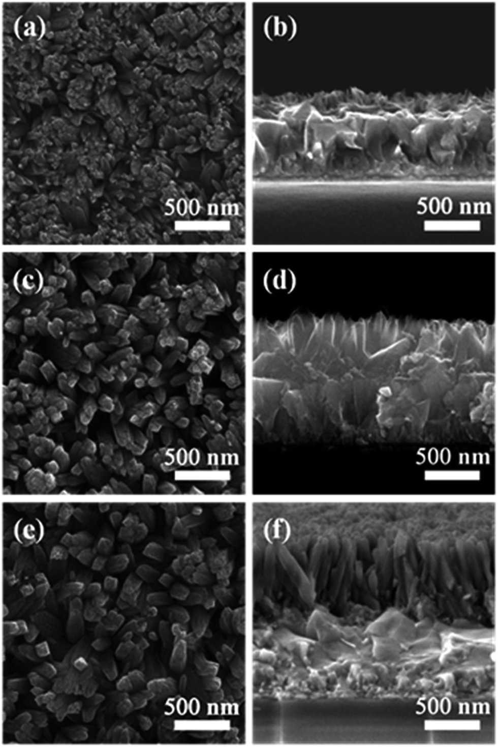 | ||
| Fig. 1 Top-view and cross-sectional SEM images of 1D RTNR arrays prepared hydrothermally with different TIP quantities showing the evolution of nanorod (NR) diameter and length: (a, b) 12.5 μL TIP (40 nm in diameter and 120 nm in length); (c, d) 25.0 μL TIP (80 nm in diameter and 600 nm in length), and (e, f) 50.0 μL TIP (120 nm in diameter and 850 nm in length). | ||
Preliminary studies of the photovoltaic performances of PSCs based on 1D RTNR arrays with different lengths were carried out and the corresponding photovoltaic parameters are presented in Table S1.† In general, the PCE increased with the increase of the RTNR length from 120 nm to 600 nm. But the PSC based on a longer RTNR (∼850 nm) exhibited decreased PCE, which is believed to be due to a declined charge generation efficiency, increased charge transport resistance as well as increased charge recombination.35 Overall, an optimal PCE of 11.15% was achieved for the PSC made from ∼600 nm long 1D RTNR.
The optimal ∼600 nm long 1D RTNR with open rod-to-rod space was subjected to a subsequent solution-processed step to construct 3D nanoarrays. As depicted in the schematic of the fabrication process in Fig. 2a, starting from the 1D vertically aligned RTNR arrays, a series of 3D array architectures (RTNR@RTB, RTNR@ATB and RTNR@Am-TB) consisting of nanorod backbones and numerous nano-branches of distinct crystal phases were formed. XRD patterns in Fig. S1† show the enhanced rutile phase characteristic peak intensities for the RTNR@RTB when compared with pristine RTNR, and mixed rutile/anatase for the RTNR@ATB, while the peak intensities were unchanged for the RTNR@Am-TB. The growth of the RTB occurred in a TiCl3/H2O/HCl solution at 80 °C for 2 h,30 ATB in a PTO/H2O/IPA/DEG solution at 190 °C for 3 h,12 and Am-TB in a PTO/H2O solution at 90 °C for 3 h.31 The crystal phase of the different TiO2 branches have been confirmed here, Fig. S1,† and further evidence is given in the previous reports.12,30,31 Specifically, it should be noted that the growth of TiO2 branches at low temperature (90 °C for 3 h, that were not annealed further) lead to the formation of amorphous TiO2, which was observed in our previous work.31 These routes for the preparation of TiO2 nanostructures with different crystal phases allow the formation of branched nanoarrays with engineered surfaces. The nano-branch density and coverage can be adjusted by varying the TiCl3 or PTO concentration, as can be seen in Fig. S2–S4.† The photovoltaic performance of PSCs based on these TiO2 array ETLs prepared with varying TiCl3 or PTO concentration are also summarized in Tables S2–S4.† The optimal morphology was achieved by using 0.2 mL TiCl3 for the RTNR@RTB, 12.5 mg PTO for RTNR@ATB or 200 mg PTO for RTNR@Am-TB.
 | ||
| Fig. 2 (a) Schematic illustration of the synthesis route for the fabrication of 3D TiO2 nanoarrays consisting of RTNR trunks and rutile, anatase or amorphous nano-branches. Top-view SEM images of (b) RTNR, (c) RTNR@RTB, (d) RTNR@ATB, and (e) RTNR@Am-TB. | ||
The 1D RTNRs have smooth sidewalls but rough top surfaces. Each large nanorod has a bundle-like morphology consisting of several slim nanorods due to a possible orientation attachment mechanism occurring during the hydrothermal process,36 (Fig. 2b). After the second hydrothermal growth step, the originally smooth 1D RTNRs are distinctly converted into 3D hierarchical tree-like architectures (Fig. 2c–e) with a large number of tiny nano-branches uniformly covering the NR surfaces. The lengths of the TiO2 branches are approximately 20–60 nm and the diameter of the TiO2 nanowires branches are approximately 10–20 nm. The diameter of the nanorods increased due to the additional branches, but the total film thicknesses of the array architectures did not change (Fig. S5†). Such 3D tree-like arrays with a high density of TiO2 nano-branches could provide a larger interfacial contact area between the perovskite and TiO2, which would enhance charge extraction.10,11 After the second-step solution-processed growth, the as-prepared RTNR@RTB and RTNR@ATB arrays were calcined in air at 500 °C for 3 h in order to improve the branch crystallinity. For the RTNR@Am-TB, no calcination was conducted (to maintain the amorphous phase of the titania branches prepared with the low temperature (90 °C) hydrothermal treatment).31 The surface of the RTNR was more evenly covered with the amorphous TiO2 coating creating the cross-linked nano-branches (Fig. 2e). The branches not only fill the interstices existing among the RTNR scaffold, but also connect the adjacent NRs together, forming a well-interconnected network, which benefits the charge transport and collection compared to non-connected branches.33
The CH3NH3PbI3 films were deposited onto the different TiO2 nanoarrays through a gas-assisted one-step spin coating method32 with slightly modified conditions. The grain size and thickness of the perovskite capping layers were governed by the different morphologies and crystal phases of the underlying TiO2 nanoarrays. The grain size distribution of the perovskite crystals and the thickness of the perovskite capping layer are summarized in Table S5.† For the 1D RTNR scaffold, larger-sized perovskite grains and a thicker capping layer (∼450 nm) were formed (Fig. 3a and b). However, pinholes were still observed in the perovskite capping layer, which increases the possibility of direct contact between the TiO2 and the HTL and hence charge recombination.37 For the 3D TiO2 nanoarrays, the increased surface area resulting from the high density of TiO2 nano-branches provides more nucleation sites for the perovskite via heterogeneous nucleation, thus forming smaller grains and thinner perovskite capping layers (300–350 nm).12 The surface coverage was slightly improved with less observable pinholes and smaller grain size (Fig. 3c and d and S6†). In addition, the 3D branched nanoarrays allowed comparatively better infiltration of the perovskite precursor solution into the mesopores within the TiO2 scaffolds than the 1D RTNR counterpart, as shown in the cross-sectional SEM images of the completed devices (Fig. 3b and d). A closer inspection of the surface SEM images of the perovskite capping layers indicates that the presence of the amorphous branches allows for the best surface coverage when compared with the crystalline rutile or anatase TiO2 branches. It is reported that the presence of higher amounts of –OH groups on the surface of amorphous TiO2 will help to improve the coordination ability with perovskite, which in turn, may lead to the growth of perovskite crystals along preferred planes, and thus possibly allow denser packing behavior.12,38,39
 | ||
| Fig. 3 Top-view SEM images of the CH3NH3PbI3 capping layer grown on (a) FTO/RTNR or (c) FTO/RTNR@Am-TNW electrodes. Cross-sectional SEM images of complete PSC devices (from bottom to top) for: (b) FTO/CH3NH3PbI3-infiltrated RTNR/CH3NH3PbI3/spiro-OMeTAD/Au and (d) FTO/CH3NH3PbI3-infiltrated RTNR@Am-TB/CH3NH3PbI3/spiro-OMeTAD/Au. | ||
To investigate the effect of the TiO2 nanoarray morphologies and compositions on the device performance, PSCs were fabricated using the aforementioned four types of 1D or 3D TiO2 nanoarray ETLs based on the device configuration of FTO/CH3NH3PbI3-infiltrated 1D or 3D TiO2 nanoarrays/CH3NH3PbI3/spiro-OMeTAD/Au. The photovoltaic performances of these PSCs were measured under AM 1.5G one sun illumination (100 mW cm−2). As shown in Fig. 4a and Table 1, the PSC with the pristine 1D RTNR array ETL showed a PCE of 11.15%. The 3D TiO2 nanoarray based PSCs exhibited higher PCEs of 12.27% for RTNR@RTB, 14.71% for RTNR@ATB and 16.06% for RTNR@Am-TB. Specifically, the Voc and FF of the 3D TiO2 nanoarray based devices were higher due to facilitated charge extraction and suppressed charge recombination compared with the 1D RTNR array counterpart (see the following photoluminescence quenching and intensity-modulated photovoltage spectroscopy characterization and discussion).10,11 A similar trend of Voc and FF enhancement has also been reported in the case of hierarchical rutile nanorods40 and core–shell ZnO@TiO2 heterostructured arrays.25 The RTNR@Am-TB showed the best photovoltaic performance with the highest Voc (1010 mV) and FF (0.73). Fig. S7† displays the incident photon-to-current conversion efficiency (IPCE) for the RTNR@Am-TB based device. The integrated current density (21.32 mA cm−2) calculated from the IPCE matched the Jsc measured under 1 sun illumination (21.80 mA cm−2) well.
 | ||
| Fig. 4 (a) J–V curves of the PSCs based on different TiO2 nanoarray ETLs. (b) Mott–Schottky plots of the different TiO2 nanoarray films. (c) Photoluminescence spectra of the perovskite films on different TiO2 nanoarray films. (d) Electron lifetime as a function of voltage for the PSCs based on different TiO2 nanoarray thin films. Note: the black, red, blue and green curves represent RTNR, RTNR@RTB, RTNR@ATB and RTNR@Am-TB in (b)–(d), respectively. | ||
In this work, the Voc and FF are strongly influenced by the morphological variation and surface properties of the various TiO2 nanoarrays. Theoretically, the Voc in solar cells is determined by the potential difference between the quasi Fermi level of the ETL and the highest occupied molecular orbital level of the HTL.41 From the Mott–Schottky plots in Fig. 4b, a gradual up-shift in the quasi Fermi energy level is observed from RTNR < RTNR@RTB < RTNR@ATB < RTNR@Am-TB as a result of increase in the charge-carrier (electron) density. This leads to a better matched energy band edge between perovskite and 3D TiO2 nanoarrays, which is believed to be beneficial for facilitating the charge extraction and collection within the corresponding cells.42 This also partially explains the notable enhancement in Voc for the PSCs based on 3D TiO2 nanoarrays.
Fig. 4c displays the photoluminescence (PL) spectra of the CH3NH3PbI3 films deposited on different TiO2 nanoarrays. A stronger PL quenching was observed in the 3D branched TiO2 array/CH3NH3PbI3 films than in the 1D RTNR nanoarray/CH3NH3PbI3 film, indicating that the photoinduced electrons in the perovskite could be more efficiently extracted by the branched TiO2 arrays. Intensity-modulated photovoltage spectroscopy (IMVS) was used to investigate charge recombination rates within the complete devices. The electron lifetime (τr) can be derived from the characteristic minimum frequency of the IMVS imaginary component. As shown in Fig. 4d, τr of the PSC based on the 3D branched TiO2 arrays is much longer than that of the 1D RTNR nanoarray based device when compared at the same voltage, indicating that the charge recombination is more effectively suppressed within the 3D branched array based devices.
These results clearly illustrate the morphological advantages of the 3D array architecture in terms of the increased interfacial contact area and the optimized band alignment between perovskite and the TiO2 ETL. Schematic illustrations of the band alignment, electron transport and charge recombination expected to occur at the different 3D TiO2 nanoarray/CH3NH3PbI3 interfaces, are depicted in Fig. 5. The advantage of the rutile structured RTNR@RTB over 1D RTNR is the enhanced internal surface area for increased interfacial contact between the TiO2 and the perovskite layer, this thus leads to slightly improved charge extraction. However, the photoinjected electrons can still recombine with the holes at the rutile TiO2/CH3NH3PbI3 interface. For the RTNR@ATB and RTNR@Am-TB arrays, in addition to the improved interfacial contact, the better energy level alignment between the CH3NH3PbI3 and TiO2 is beneficial for the electron–hole separation and facilitates charge extraction. Furthermore, the conduction band edge offset of the rutile trunk/anatase branches or rutile trunk/amorphous branches provides an energy level cascade, favoring electron transfer in the branched array ETLs. Moreover, the layer of ATNW nano-branches or Am-TNW nano-branches could create an interfacial energy barrier to minimize the back-flow of electrons from the conduction band of the RTNR trunk to the perovskite and thus retard the charge recombination. This was confirmed by the increased dark current onset (Fig. 4a) and prolonged electron lifetime (Fig. 4d) for the PSCs based on RTNR@ATNW and RTNR@Am-TNW ETLs. Surprisingly, the most efficient charge extraction and effective charge recombination suppression was observed in the RTNR@Am-TNW based devices. Compared with the crystalline ATNW branches, the well-interconnected and cross-linked amorphous branched networks, which link the adjacent trunks and branches, helped to efficiently extract the photogenerated electrons from the perovskite to the ETL.33,43 Moreover, amorphous TiO2 branches that provide good surface coverage are believed to be capable of passivating the surface defects and trap states on the RTNR trunk, thus hindering the charge recombination at the interface. The thin amorphous branched layers would ensure a reduction in the passivation layer film capacitance, resulting in devices with higher open-circuit voltage.20,23 Overall, the increased Voc and FF for the RTNR@Am-TB based devices resulted cumulatively from the charge recombination reduction, surface passivation, as well as interfacial resistance minimization due to the rutile/amorphous interface.
 | ||
| Fig. 5 Schematic illustrations of band alignment, electron transport and charge recombination behavior at the ETL/perovskite interface based on the 3D array architectures, where R, A and Am indicate rutile, anatase and amorphous phases respectively. | ||
PSCs often exhibit hysteresis in their J–V curves.44 The J–V curves for the PSCs based on the four types of TiO2 nanoarrays studied here were measured under both reverse and forward voltage scan directions with a scan rate of 0.1 V s−1 (Fig. S8†) and the photovoltaic parameters are summarized in Table S6.† The 3D TiO2 nanoarrays were effective in minimizing the hysteresis. The RTNR@Am-TB based device had the lowest hysteresis, which could be ascribed to the facilitated charge extraction, suppressed charge recombination, as well as a beneficial surface passivation effect within this cell.13,25 In order to accurately evaluate the performance of the PSC based on RTNR@Am-TB, the stabilized power output under load near the maximum power point was measured. As shown in Fig. S9,† the best-performing cell exhibited a stabilized PCE of ∼15.50% under a bias voltage of 0.82 V, which is close to the highest efficiency obtained from the derived J–V sweep (Fig. 4a and Table 1).
Conclusions
In summary, a solution-processed branch modification strategy was developed for the preparation of 3D RTNR@RTB as well as RTNR@ATB and RTNR@Am-TB nanoarray architectures, in which the rutile, anatase or amorphous titania nano-branches grew off the RTNR backbone. When used as ETLs in PSCs, the 3D TiO2 arrays have shown benefit in terms of the enlarged interfacial contact area between the perovskite and TiO2, which results in improved charge extraction. The rutile@anatase and rutile@amorphous structures raised the quasi Fermi energy level of the TiO2 array ETLs and thus improved the band alignment with the perovskite, which provides an energy cascade favoring extraction and transport of the electron from the perovskite layer to the TiO2 branches and trunks. The difference in the conduction band edge between the trunk and branches also served as an interfacial energy barrier to effectively block the electron back reaction. As a result, a notably improved photovoltaic performance (reaching a PCE of 16.06% and with less hysteresis) was attained by optimizing the array constituents with the combination of rutile trunk and amorphous nano-branches. This can be attributed to the synergistic effects of the facilitated charge extraction, suppressed charge recombination and beneficial surface passivation within the RTNR@Am-TB based devices. It is expected that the photovoltaic performance could be further improved if optimized perovskite light harvesting materials were incorporated with the heterocrystalline TiO2 nanoarrays. In particular, this work illustrates the design of various 3D inorganic semiconductor array architectures with engineered structures that show potential in energy conversion.Conflicts of interest
There are no conflicts to declare.Acknowledgements
W. Q. W. acknowledges the Albert Shimmins Fund for a postgraduate writing up award. The Melbourne Advanced Microscopy Facility at The University of Melbourne provided access to electron microscopy facilities. Support from the Australian Renewable Energy Agency, The Australian Centre for Advanced Photovoltaics and the ARC Centre of Excellence in Exciton Science (CE170100026) is acknowledged. R. A. C. acknowledges the Australian Research Council for a Future Fellowship (FT0990583).Notes and references
- J. Burschka, N. Pellet, S. J. Moon, R. Humphry-Baker, P. Gao, M. K. Nazeeruddin and M. Grätzel, Nature, 2013, 499, 316–319 CrossRef CAS PubMed.
- M. Z. Liu, M. B. Johnston and H. J. Snaith, Nature, 2013, 501, 395–398 CrossRef CAS PubMed.
- J. H. Heo, S. H. Im, J. H. Noh, T. N. Mandal, C. S. Lim, J. A. Chang, Y. H. Lee, H. J. Kim, A. Sarkar, M. K. Nazeeruddin, M. Grätzel and S. I. Seok, Nat. Photonics, 2013, 7, 487–492 CrossRef.
- M. D. Xiao, F. Z. Huang, W. C. Huang, Y. Dkhissi, Y. Zhu, J. Etheridge, A. Gray-Weale, U. Bach, Y. B. Cheng and L. Spiccia, Angew. Chem., Int. Ed., 2014, 53, 9898–9903 CrossRef CAS PubMed.
- A. Kojima, K. Teshima, Y. Shirai and T. Miyasaka, J. Am. Chem. Soc., 2009, 131, 6050–6051 CrossRef CAS PubMed.
- http://www.nrel.gov/ncpv/images/efficiency_chart.jpg .
- N. J. Jeon, J. H. Noh, Y. C. Kim, W. S. Yang, S. Ryu and S. I. Seol, Nat. Mater., 2014, 13, 897–903 CrossRef CAS PubMed.
- W. J. Ke, G. J. Fang, J. W. Wan, H. Tao, Q. Liu, L. B. Xiong, P. L. Qin, J. Wang, H. W. Lei, G. Yang, M. C. Qin, X. Z. Zhao and Y. F. Yan, Nat. Commun., 2015, 6, 6700 CrossRef CAS PubMed.
- W.-Q. Wu, F. Huang, D. Chen, Y.-B. Cheng and R. A. Caruso, Adv. Energy Mater., 2016, 6, 1502027 CrossRef.
- Y. Yu, J. Li, D. Geng, J. Wang, L. Zhang, T. L. Andrew, M. S. Arnold and X. Wang, ACS Nano, 2015, 9, 564–572 CrossRef CAS PubMed.
- K. Mahmood, B. S. Swain and A. Amassian, Adv. Mater., 2015, 27, 2859–2865 CrossRef CAS PubMed.
- W. Q. Wu, F. Z. Huang, D. H. Chen, Y. B. Cheng and R. A. Caruso, Adv. Funct. Mater., 2015, 25, 3264–3272 CrossRef CAS.
- K. Mahmood, B. S. Swain and A. Amassian, Adv. Energy Mater., 2015, 5, 1500568 CrossRef.
- L. Zuo, Z. Gu, T. Ye, W. Fu, G. Wu, H. Li and H. Chen, J. Am. Chem. Soc., 2015, 137, 2674–2679 CrossRef CAS PubMed.
- Q. Jiang, X. Sheng, Y. Li, X. Feng and T. Xu, Chem. Commun., 2014, 50, 14720–14723 RSC.
- H. S. Kim, J. W. Lee, N. Yantara, P. P. Boix, S. A. Kulkarni, S. Mhaisalkar, M. Grätzel and N. G. Park, Nano Lett., 2013, 13, 2412–2417 CrossRef CAS PubMed.
- P. Qin, M. Paulose, M. I. Dar, T. Moehl, N. Arora, P. Gao, O. K. Varghese, M. Grätzel and M. K. Nazeeruddin, Small, 2015, 11, 5533–5539 CrossRef CAS PubMed.
- D. Zhong, B. Cai, X. Wang, Z. Yang, Y. Xing, S. Miao, W.-H. Zhang and C. Li, Nano Energy, 2015, 11, 409–418 CrossRef CAS.
- D. Bi, L. Yang, G. Boschloo, A. Hagfeldt and E. M. J. Johansson, J. Phys. Chem. Lett., 2013, 4, 1532–1536 CrossRef CAS PubMed.
- A. K. Chandiran, A. Yella, M. T. Mayer, P. Gao, M. K. Nazeeruddin and M. Grätzel, Adv. Mater., 2014, 26, 4309–4312 CrossRef CAS PubMed.
- H.-S. Rao, B.-X. Chen, W.-G. Li, Y.-F. Xu, H.-Y. Chen, D.-B. Kuang and C.-Y. Su, Adv. Funct. Mater., 2015, 25, 7200–7207 CrossRef CAS.
- T. C. Li, M. S. Góes, F. Fabregat-Santiago, J. Bisquert, P. R. Bueno, C. Prasittichai, J. T. Hupp and T. J. Marks, J. Phys. Chem. C, 2009, 113, 18385–18390 CAS.
- S. S. Mali, C. S. Shim, H. K. Park, J. Heo, P. S. Patil and C. K. Hong, Chem. Mater., 2015, 27, 1541–1551 CrossRef CAS.
- B. C. O'Regan and J. R. Durrant, Acc. Chem. Res., 2009, 42, 1799–1808 CrossRef PubMed.
- K. Mahmood, B. S. Swain and A. Amassian, Nanoscale, 2015, 7, 12812–12819 RSC.
- X. Xu, H. Zhang, J. Shi, J. Dong, Y. Luo, D. Li and Q. Meng, J. Mater. Chem. A, 2015, 3, 19288–19293 CAS.
- M. M. Lee, J. Teuscher, T. Miyasaka, T. N. Murakami and H. J. Snaith, Science, 2012, 338, 643–647 CrossRef CAS PubMed.
- A. Y. Mei, X. Li, L. F. Liu, Z. L. Ku, T. F. Liu, Y. G. Rong, M. Xu, M. Hu, J. Z. Chen, Y. Yang, M. Grätzel and H. W. Han, Science, 2014, 345, 295–298 CrossRef CAS PubMed.
- W. Chen, Y. Wu, J. Liu, C. Qin, X. Yang, A. Islam, Y.-B. Cheng and L. Han, Energy Environ. Sci., 2015, 8, 629–640 CAS.
- X. Sheng, D. Q. He, J. Yang, K. Zhu and X. J. Feng, Nano Lett., 2014, 14, 1848–1852 CrossRef CAS PubMed.
- W.-Q. Wu, D. Chen, F. Huang, Y.-B. Cheng and R. A. Caruso, J. Power Sources, 2016, 329, 17–22 CrossRef CAS.
- F. Huang, Y. Dkhissi, W. Huang, M. Xiao, I. Benesperi, S. Rubanov, Y. Zhu, X. Lin, L. Jiang, Y. Zhou, A. Gray-Weale, J. Etheridge, C. R. McNeill, R. A. Caruso, U. Bach, L. Spiccia and Y.-B. Cheng, Nano Energy, 2014, 10, 10–18 CrossRef CAS.
- W. Q. Wu, H. L. Feng, H. S. Rao, Y. F. Xu, D. B. Kuang and C. Y. Su, Nat. Commun., 2014, 5, 3968 CAS.
- B. Liu and E. S. Aydil, J. Am. Chem. Soc., 2009, 131, 3985–3990 CrossRef CAS PubMed.
- H. S. Kim, C. R. Lee, J. H. Im, K. B. Lee, T. Moehl, A. Marchioro, S. J. Moon, R. Humphry-Baker, J. H. Yum, J. E. Moser, M. Gratzel and N. G. Park, Sci. Rep., 2012, 2, 591 CrossRef PubMed.
- R. Zeng, K. Li, X. Sheng, L. Chen, H. Zhang and X. Feng, Chem. Commun., 2016, 52, 4045–4048 RSC.
- G. C. Xing, N. Mathews, S. Y. Sun, S. S. Lim, Y. M. Lam, M. Grätzel, S. Mhaisalkar and T. C. Sum, Science, 2013, 342, 344–347 CrossRef CAS PubMed.
- E. Mosconi, E. Ronca and F. De Angelis, J. Phys. Chem. Lett., 2014, 5, 2619–2625 CrossRef CAS PubMed.
- C. Tao, S. Neutzner, L. Colella, S. Marras, A. R. Srimath Kandada, M. Gandini, M. D. Bastiani, G. Pace, L. Manna, M. Caironi, C. Bertarelli and A. Petrozza, Energy Environ. Sci., 2015, 8, 2365–2370 CAS.
- O. A. Jaramillo-Quintero, M. Solis de la Fuente, R. S. Sanchez, I. B. Recalde, E. J. Juarez-Perez, M. E. Rincon and I. Mora-Sero, Nanoscale, 2016, 8, 6271–6277 RSC.
- K. Wang, Y. Shi, B. Li, L. Zhao, W. Wang, X. Wang, X. Bai, S. Wang, C. Hao and T. Ma, Adv. Mater., 2015, 28, 1891–1897 CrossRef PubMed.
- R. O'Hayre, M. Nanu, J. Schoonman and A. Goossens, J. Phys. Chem. C, 2007, 111, 4809–4814 Search PubMed.
- W. Q. Wu, Y. F. Xu, H. S. Rao, C. Y. Su and D. B. Kuang, J. Am. Chem. Soc., 2014, 136, 6437–6445 CrossRef CAS PubMed.
- H. J. Snaith, A. Abate, J. M. Ball, G. E. Eperon, T. Leijtens, N. K. Noel, S. D. Stranks, J. T. W. Wang, K. Wojciechowski and W. Zhang, J. Phys. Chem. Lett., 2014, 5, 1511–1515 CrossRef CAS PubMed.
Footnote |
| † Electronic supplementary information (ESI) available. See DOI: 10.1039/c7se00377c |
| This journal is © The Royal Society of Chemistry 2017 |