
Shape-controlled electrochemical synthesis of mesoporous Si/Fe nanocomposites with tailored ferromagnetic properties†
B.
Bardet
 a,
T.
Defforge
a,
B.
Negulescu
a,
D.
Valente
a,
J.
Billoué
a,
P.
Poveda
b and
G.
Gautier
*a
a,
T.
Defforge
a,
B.
Negulescu
a,
D.
Valente
a,
J.
Billoué
a,
P.
Poveda
b and
G.
Gautier
*a
aUniversité François Rabelais de Tours, CNRS, CEA, INSA-CVL, GREMAN UMR 7347, 16 rue Pierre et Marie Curie, 37071 Tours, France. E-mail: gael.gautier@univ-tours.fr
bSTMicroelectronics Tours, 16 rue Pierre et Marie Curie, 37071 Tours, France
First published on 30th August 2016
Abstract
This study reports on an original and efficient way to synthesize iron nanowires and cubic-shaped nanoparticles by electrochemical deposition on a mesoporous silicon host and its impact on magnetic properties. The selective growth of iron nanostructures inside the pores can be achieved, thanks to the presence of a native oxide layer on the pore walls, suggesting a surface-state assisted electrochemical process. Because of hydrogen coevolution, the pH of the solution controls the shape of the iron nanostructures (particles or wires) while the electrodeposition current density can be adjusted to suppress the parasitic deposition on top of the structure. Under optimal conditions, nanowires with lengths up to 2 μm are synthesized after 15 seconds of deposition. Magnetic characterization of the ferromagnetic nanowire composite exhibits an easy axis of magnetization in the pore direction due to shape anisotropy with a remanence ratio of 0.6. The shape anisotropy of the nanoparticle composite is weaker than for the nanowire composite because of the homogeneous dispersion of the particles. The versatility of the mesoporous silicon framework is thus a considerable asset to tune the nanocomposite’s magnetic properties.
Introduction
Besides data storage applications,1 iron-based nanostructures present a specific interest for many applicative domains such as biomedicine,2 Li-ion batteries3 and high-frequency electronics.4 The large diversity of iron oxides and iron alloys opens up the scope of possibilities. In addition to the intrinsic physical properties of the magnetic material, special effort must be applied to control its shape, its size and also its orientation in order to get maximum benefit from anisotropic effects.5 Therefore, the use of an appropriate host material becomes a critical parameter. Due to its controllable size and shape6 and its versatility, the incorporation of magnetic nano-objects in mesoporous silicon (PS) is nowadays a crucial topic. For instance, the great interest of PS as a magnetic nanoparticle carrier for applications in magnetic resonance imaging or drug delivery has been recently demonstrated.7,8However, the insertion of magnetic nanostructures into a PS host remains a challenging task. Nanoparticles can be synthesized and then inserted into mesostructured silicon by sonication,9,10 but this technique is not suitable for large particles (size roughly comparable to the pore diameter) or nanowires. To date, electrochemical deposition has been seen as the most efficient approach to synthesize such mesoscopic structures in a porous medium. For instance, promising PS–nickel composites were synthesized by electrodeposition that provide adjustable ferromagnetic properties depending on the properties of the PS host.11–14 However, these results could not be replicated with PS–Fe composites because the deposition takes place preferentially on top of the porous layer instead of entering the pores, as reported by all studies published on this topic.15–17 As a result, the magnetic contribution of the iron nanostructure cannot be distinguished from the one of the surface deposit. In addition, this issue is especially critical for thin-film processing as a low surface roughness is required in a conventional process.
This work aims to fulfill two objectives. The first one is to suggest a strategy to synthesize both iron nanoparticles and iron nanowires in a 4 μm-thick mesoporous silicon host without any parasitic surface deposition. The pore surface chemistry, electrolyte composition, and deposition current density are adjusted to reach this goal. Their influence is discussed considering the interfacial electrochemical mechanisms. The second objective is to study the impact of the iron inclusion morphology (nanowires or nanoparticles) on the magnetic properties of the composites. Hysteresis magnetization loops are measured in plane and out of plane using a vibrating sample magnetometer. The magnetic behavior of the different structures is also discussed as a function of the morphology.
Experimental
PS formation
PS layers are obtained by electrochemical etching of 6 inch low-resistivity (10–15 mΩ cm) n-type (100) monocrystalline silicon wafers in a double-tank cell. The electrolyte is a mixture of water, hydrofluoric acid (HF) with a concentration of 5% in weight and Triton™ X-100 acting as a wetting agent. To obtain acceptable pore openings (e.g. higher than 20 nm) and straight vertical pores, the applied current density is chosen relatively high, that is to say close to the electropolishing regime.18,19 A galvanostatic regime is employed with a current density of 25 mA cm−2. The duration is adjusted to obtain 4 μm-thick PS layers with a porosity approximately equal to 66%. Porosity measurements are carried out by gravimetry. After the anodization, the wafers are thoroughly rinsed in deionized water and dried in a Semitool spin rinse dryer. The wafers are then cut into 3 × 3 cm2 samples.Synthesis of iron nanostructures in PS
The iron nanoparticles are synthesized by electrochemical deposition onto the PS layer. Indeed, iron salts are directly reduced to their metallic form on the corrugated pore sidewalls (cf.Fig. 1a). This operation is performed in an electrochemical cell using a three-electrode setup. A copper strip is stuck on the rear side of the PS cathode to obtain an efficient ohmic contact. A platinum disk plays the role of the anode whereas a saturated calomel electrode (SCE) is used as a reference electrode. Every electrode potential reported in this study is relative to the potential of the SCE electrode.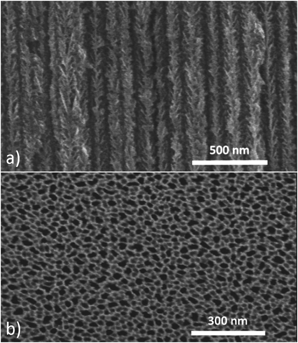 | ||
| Fig. 1 SEM views of the 66% porosity PS sample in (a) cross-section and (b) top view. | ||
Iron is electrodeposited from an electrolyte composed of 0.1 M FeSO4·7H2O (as a source of Fe2+ ions), ammonium lauryl sulfate (ALS), saccharine and acetic acid. ALS is used as a wetting agent; it helps to evacuate hydrogen bubbles from the pores and thus improves the renewal of the electrolyte in the porous layer. This molecule is known to be compatible with iron-based plating solutions.20 Acetic acid is used as a pH stabilizer,21 in the pH range of 1 to 3, instead of the more common boric acid.22–24 The substitution of boric acid by acetic acid is motivated by the guidance of the European Union's chemical regulations on carcinogenic, mutagenic and reprotoxic chemicals (CMR) which classify boric acid in the CMR1B category.25 Prior to electrodeposition, PS is impregnated with the electrolyte and sonicated for 15 minutes to ensure optimal penetration of the solution. A constant current density in the milliampere range is applied to synthesize iron particles in the pores with durations varying from a few seconds to a few minutes using a SP150 Bio-Logic galvanostat. The influence of duration, current density and electrolyte pH is specifically investigated in order to adjust the morphology of the iron nanostructures. After iron electrodeposition, the PS–Fe nanocomposite is rinsed in deionized water and dried on a hot plate at 120 °C.
Characterization tools
A Bruker Vertex 70v FT-IR spectrometer enables the chemical characterization of PS prior to deposition. High-resolution scanning electron microscopy (SEM) images of PS layers and PS–Fe composites are taken in top (0°), tilted (75°) and cross-sectional views (90°) using a Hitachi S-4160 or a FEI Strata 400S. To enhance the chemical contrast between iron and silicon, back-scattered electron (BSE) and energy-dispersive X-ray spectroscopy (EDX) detectors are employed in addition to a conventional secondary electrons detector (SE). A vibrating sample magnetometer (VSM) inserted into a Quantum Design PPMS is used to obtain magnetization hysteresis loops. Magnetic fields, between −1.5 T and 1.5 T, were applied successively in parallel (in plane) or perpendicularly (out of plane) to the sample surface to detect any anisotropic phenomena. The iron-based PS composite is characterized by X-ray diffraction (XRD) using a D8 Bruker powder diffractometer (λCu = 1.54 Å) over a 2θ range of 20° to 90° with a step of 0.02°.Results and discussion
Electrochemical deposition of iron nanostructures
The aim of this section is to describe an original method to synthesize homogenous PS–Fe nanocomposites, i.e. without any deposition on the layer surface. This selective process is found to be directly dependent on the surface chemistry of the silicon pore sidewalls, the pH of the electrolyte and the current density. The overall observed tendencies are put in perspective with electrochemical phenomena.Influence of PS surface chemistry
Generally, in order to deposit iron on silicon (planar or nanostructured), the surface is usually deoxidized prior to the cathodic process.26–28 Hydrogen-terminated silicon provides a low surface energy on which three-dimensional nucleation can occur owing to weak metal–silicon interactions. Once the first germs nucleate, growth prevails on the adsorbed particles. However, iron reduction inside PS is rendered difficult by the low fraction of nucleation sites inside the porous medium. In fact, previous studies on iron deposition in PS show that nucleation occurs inside the pores as well as on the surface of PS leading to large undesirable amounts of iron on the surface.16,17,29,30In this study, we also observe this phenomenon. The electrochemical deposition of iron on a hydrogen-terminated PS sample leads to a preferential growth of iron clusters on top of the sample. SEM views in SE and BSE modes highlight this behavior (Fig. 2).
 | ||
| Fig. 2 Tilted SEM views of the PS–Fe composite starting from a hydrogen-terminated PS surface using (a) a SE detector and (b) a BSE detector. Deposition of iron is performed at 6 mA cm−2 for 2.7 minutes. pH is fixed at 1.8. White spots represent iron particles. | ||
The density of iron clusters inside the pores is lower than on top of the structure. In fact, the presence of this rough thin-film formation on top of the layer could be a critical issue. On one hand, it would screen the interest of the composite and, on the other hand, it would hinder any subsequent microelectronic thin-film process by roughening the surface. As a result, the first objective is to selectively increase the density of iron nuclei inside the pores to avoid the formation of a parasitic film on top of the structure.
In this paper, a modification of the PS surface chemistry is suggested as an option to selectively grow iron in the porous matrix. For that purpose, a PS sample with the same characteristics as previously reported is dried and then stored in air for two weeks before the electrochemical deposition step. So a thin native oxide is present on the pore walls. Under similar electrochemical conditions, iron particles are deposited on this oxidized sample. SEM tilted views of the composite are shown in Fig. 3. The potential transients measured during the galvanostatic deposition are shown in Fig. S1 (ESI†).
 | ||
| Fig. 3 Tilted SEM views of the PS–Fe composite starting from an aged PS surface covered by a native oxide using (a) a SE detector and (b) a BSE detector. Deposition of iron was done at 6 mA cm−2 for 2.7 minutes. pH was fixed at 1.8. White spots represent iron particles. | ||
SEM views show a high density of randomly dispersed particles in the aged PS host (Fig. 3) which is a first significant improvement. The second advantage of this structure is the absence of large amounts of particles on top of the layer. So, the native oxide layer that covers the silicon crystallites seems to favor the deposition inside the porous structure.
To investigate the origin of such differences, the surface chemistry is characterized by means of transmission FT-IR spectroscopy (Fig. 4).
 | ||
| Fig. 4 FTIR transmittance spectra of PS samples measured immediately after drying (black curve) and after two weeks (red curve). The sample is deoxidized by HF dip, rinsed in deionized water, dried and immediately measured. After two weeks at room temperature, the measurement is repeated at the same location. Labels are added to identify vibration modes related to PS surface chemistry. | ||
Immediately after drying, the pore sidewalls are covered with hydrogen due to the chemical etching in HF. Silicon hydrides (SiHx with x = 1, 2, or 3) are detected, thanks to their characteristic stretching bands ν(SiH3) = 2140 cm−1, ν(SiH2) = 2114 cm−1 and ν(SiH) = 2090 cm−1.31 After ageing, absorption of OySiHx (with (x,y) = 1, 2, or 3) and a broad SiOH absorption area strongly increase which indicate a native oxide growth on the pore walls.32,33 A carbon-related contamination at ν(CH2) = 2860 cm−1, ν(CH2) = 2921 cm−1, ν(CH3) = 2960 cm−1 is also visible which originates from atmospheric pollution.34,35 The adsorption on silicon of hydroxyl groups and carbon compounds coupled to the unsaturated bonds at the silicon–silicon oxide interface is known to provide a high density of surface states.36,37 As a result, the electronic behavior of the silicon–electrolyte interface during metal electrodeposition changed. If the rate of charge transfer from the surface states is sufficiently high, then these surface states could act as nucleation sites for metal deposition.26 The high specific surface area of PS due to the small pore size and PS sidewall waviness necessarily reinforces this trend. This surface-state catalysis hypothesis correlates to some extent with the study of Hamadache and coworkers dealing with the deposition of FeCo on PS.15 The addition of cobalt salts in the electrolyte enhanced the nucleation rate preferentially inside the pores. As cobalt is easily reduced on the silicon pore walls, absorbed cobalt atoms act as surface states and provide nucleation sites for iron co-deposition.
Therefore, the introduction of extrinsic surface states at the semiconductor–electrolyte interface is a significant advantage to selectively deposit iron nanostructures inside the pores. In fact, this approach has some similitudes with nanopatterning techniques based on defect generation on silicon proposed by Schmuki's group in the early 2000's.38,39
In the following sections, native oxide is always kept on the pore walls. Iron deposition is carried out after a subsequent period of two weeks after the electrochemical etching of silicon. The aim of the next section is to describe the synthesis of various nanostructures (nanowires, nanoparticles) by adjusting different electrochemical parameters, such as the current density and the pH of the electrolyte.
Impact of pH
Another key parameter for the control of iron deposition is the acidity of the solution. Contrary to noble metals, iron deposition takes place with a low Coulombic efficiency owing to the low equilibrium potential of Fe2+/Fe compared to H+/H2. Therefore, hydrogen bubbling occurs as a concomitant reaction of iron deposition, eqn (1), (2). Low pH electrolytes (pH < 1) are expected to induce low Coulombic efficiency electrodeposition whereas less acidic electrolytes (pH > 3) are known to produce iron(III) hydroxide precipitates that cause a decrease of magnetization.24,40,41 So, the pH must be adjusted cautiously. | (1) |
 | (2) |
 | ||
| Fig. 5 SEM cross-sectional views of composites synthesized at 7.5 mA cm−2 for 2 minutes. pH of the electrolyte is 1.6 (a and c) or 2.2 (b and d). pH is adjusted by the addition of acetic acid. (a) and (b) are BSE tilted views, while (c) and (d) are SE high-magnification cross-sectional views of (a) and (b), respectively. | ||
Iron particles do not present the same shape and size depending on the pH of their respective electrolyte. Clusters are elongated along the pore direction with the pH 2.2 solution (Fig. 5b and d) whereas cubic and isolated iron particles are formed when using the pH 1.6 solution. The elongated particles are composed of many metal crystallites which aggregate to form a single nanowire. Its length reaches 2 μm whereas its mean diameter varies in the range 40–80 nm. The size of cubic particles obtained with the low pH solution is about 80 nm. Hydrogen bubbling is presumably the reason why the particles have the same shape and size. The formation and release of H2 bubbles produce a convective mixing that locally enhances the mass transport and thus tends to reduce the interparticle coupling.43–45 At pH 2.2 (and higher), hydrogen evolution is not as strong as at pH 1.6, so the Coulombic efficiency of the electrodeposition is slightly higher. As a result, growth occurs on iron nuclei and the formation of elongated structures is observed.
Impact of current density
In a large range of applications, the presence of particles or agglomerates on the top surface of the composite can cancel the beneficial effect of the PS–Fe composite. As a result, any iron particles on top of the PS layer should be completely avoided. When a high pH electrolyte and a low current density are used, 10 μm thick iron spots randomly appear on top of the structure as depicted in Fig. 6a. An optimal current density must be determined at which no cluster grows on the surface. To facilitate the comparison between the samples, the deposition was carried out under a galvanostatic regime, while keeping the injected charge constant. SEM and BSE cross-sectional views of the PS–Fe composites are depicted in Fig. 6. | ||
| Fig. 6 SEM tilted views in SE mode (a), (c) and (e) and cross-section views in BSE mode (b), (d) and (f) of PS–Fe composites synthesized at three different current densities using the same electrolyte (pH = 2.2). Tilted views show the deposition on the surface whereas the cross-sectional views highlight the presence of nanowires inside the pores. | ||
After electrodeposition at high current density (e.g. 25 mA cm−2 for 7.5 s), the micrometer-sized iron clusters disappear from the surface and are replaced by smaller clusters (D ≈ 100 nm) with quite homogeneous sizes (cf.Fig. 6e). BSE analysis also shows a high particle density inside the pores. Intermediate current density (12.5 mA cm−2 for 15 s) yields a surface free of iron particles while keeping a significant particle density in the porous media. The increase of current thus seems to promote the deposition of iron nanowires at the PS–Si interface. At high current density, the deposition overpotential is high (E < −3 V/ECS). An electric field enhancement at the PS–Si interface could explain this behavior.
These results show that the morphology of the PS–Fe composites can be controlled by adjusting the surface chemistry of the crystallites, the pH of the electrolyte and the current density of the electrochemical deposition of iron. The validity of this technique was checked using different PS samples with various pore sizes from 30 nm to 120 nm. The diameter of the NWs and the size of the NPs fit well with the pore diameter of the starting PS layer (see Fig. S2, ESI†). These tendencies allow us to form two optimal composites without any deposit on the surface. The conditions selected to synthesize the PS–Fe nanoparticle composite (PS–FeNPs) are an electrolyte of pH 1.6, a current density of 7.5 mA cm−2 and a duration of 120 s. The PS–Fe nanowire composite (PS–FeNWs) is obtained from an electrolyte of pH 2.2, a 12.5 mA cm−2 current density and a duration of 15 s.
PS–Fe composite characterization
 | ||
| Fig. 7 X-Ray diffraction patterns of the PS–NWs and PS–NPs composites. Miller indices of iron are extracted from bcc α-Fe (JCPDS 06-0696). | ||
The (200) and (211) peaks are not sufficiently intense to be accurately analyzed. However, the (110) peak broadening can be studied to determine an average crystallite size. The broadening due to the equipment is estimated from a reference sample and then subtracted from the total broadening. A Voigt function is employed to fit the (110) peak broadening of iron in order to deconvolute the broadening due to crystallite size, and the broadening attributed to stress.47 Average crystallite sizes of 32 nm and 59 nm are measured for FeNPs and FeNWs respectively.
 | ||
| Fig. 8 Normalized magnetization loops measured at 300 K in plane (black) and out of plane (red) for three different composites: (a) PS–FeNPs + parasitic layer (b), PS–FeNPs (c) and PS–FeNWs. The corresponding inset shows a schematic representation of the composite morphology. | ||
The magnetic behavior of the PS–FeNP and PS–FeNW composites is different (Fig. 8b and c). The detailed magnetic parameters of these two samples are given in Table S1 (ESI†). Both composites demonstrate a preferential magnetization along the pore direction. The anisotropy field (HA) is defined as the minimum field to apply in order to align the magnetic moments in the hard axis of magnetization. The value of HA (1 T) observed on the PS–FeNW sample is consistent with computed values of infinite iron wires,48 a sign of the high aspect ratio of the nanowires (see EDX mapping in Fig. S3 (ESI†) and the BSE SEM view in Fig. 6d). The anisotropy on this structure is assumed to originate from the shape of the iron inclusions whereas magnetocrystalline anisotropy and stress can be neglected.48 The remanence–saturation ratio (MR/MS = 0.6) is similar to the one for nanowires grown through an ordered porous alumina matrix.24,48,49 The porous framework is thus a very efficient template to create anisotropic structures because a single nanowire or disoriented structures do not exhibit such a behavior.46 The magnetic anisotropy of the PS–FeNP composite is less significant compared to the PS–FeNWs. The in-plane anisotropy field is around 0.65 T and the remanence–saturation ratio is 0.25. This quasi-isotropic behavior could be justified by the homogeneous repartition of NPs observed in the SEM views. (cf.Fig. 5a and c). Therefore, it is possible to selectively synthesize iron nanostructures inside the pores in order to tune the magnetic anisotropy.
Conclusion
The selective electrodeposition of iron nanostructures inside a host PS medium can be performed by adjusting the surface chemistry of the PS sidewalls. The hydrogen-terminated surface of PS is intentionally replaced by an aged and oxidized surface. The adsorption of atmospheric contaminants and the oxidation of the corrugated pore wall tend to enhance its chemical reactivity by providing singularities on which iron nucleation preferentially occurs. As a result, FeNPs are selectively synthesized inside the PS matrix. Because the equilibrium potential of Fe/Fe2+ is very low, hydrogen co-evolution is catalysed on iron germs and tends to equalize the NP sizes. The synthesis of homogeneously dispersed nanoparticles with cubic shape is a significant advantage of using PS as a host matrix instead of an insulating matrix. An increase in pH is sufficient to produce high aspect ratio nanowires with lengths up to 2 μm. The parasitic deposit on top can be avoided by adjusting the current density. Magnetization hysteresis loops of the composites highlight a marked shape anisotropy in the PS–FeNWs composite. Remanence, anisotropy, and coercivity are found to be quite similar to the results reported in the literature for FeNWs grown through a porous alumina template. On the other hand, the nanoparticle composite demonstrates a quasi-isotropic behavior. These results highlight the good versatility of the mesoporous silicon framework and pave the way for further studies on semiconductor/iron-based ferromagnetic nanocomposites.Acknowledgements
This work was performed in the frame of TOURS 2015, a project supported by the French “Programme de l'économie numérique des Investissements d'Avenir”.References
- C. Chappert, A. Fert and F. N. Van Dau, Nat. Mater., 2007, 6, 813–823 CrossRef CAS PubMed.
- M. Liong, J. Lu, M. Kovochich, T. Xia, S. G. Ruehm, A. E. Nel, F. Tamanoi and J. I. Zink, ACS Nano, 2008, 2, 889–896 CrossRef CAS PubMed.
- P. L. Taberna, S. Mitra, P. Poizot, P. Simon and J.-M. Tarascon, Nat. Mater., 2006, 5, 567–573 CrossRef CAS PubMed.
- B. K. Kuanr, V. Veerakumar, R. Marson, S. R. Mishra, R. E. Camley and Z. Celinski, Appl. Phys. Lett., 2009, 94, 202505 CrossRef.
- E. Araujo, A. Encinas, Y. Velázquez-Galván, J. M. Martínez-Huerta, G. Hamoir, E. Ferain and L. Piraux, Nanoscale, 2015, 7, 1485–1490 RSC.
- R. Herino, G. Bomchil, K. Barla, C. Bertrand and J. L. Ginoux, J. Electrochem. Soc., 1987, 134, 1994 CrossRef CAS.
- J. M. Kinsella, S. Ananda, J. S. Andrew, J. F. Grondek, M.-P. Chien, M. Scadeng, N. C. Gianneschi, E. Ruoslahti and M. J. Sailor, Adv. Mater., 2011, 23, H248–H253 CrossRef CAS PubMed.
- L. Gu, J.-H. Park, K. H. Duong, E. Ruoslahti and M. J. Sailor, Small, 2010, 6, 2546–2552 CrossRef CAS PubMed.
- F. A. Harraz, Appl. Surf. Sci., 2013, 287, 203–210 CrossRef CAS.
- P. Granitzer, K. Rumpf, R. Gonzalez-Rodriguez, J. L. Coffer and M. Reissner, Nanoscale, 2015, 7, 20220–20226 RSC.
- K. Rumpf, P. Granitzer, N. Koshida, P. Poelt and H. Michor, ECS J. Solid State Sci. Technol., 2015, 4, N41–N43 CrossRef CAS.
- A. L. Dolgiy, S. V. Redko, I. Komissarov, V. P. Bondarenko, K. I. Yanushkevich and S. L. Prischepa, Thin Solid Films, 2013, 543, 133–137 CrossRef CAS.
- P. Granitzer, K. Rumpf, T. Ohta, N. Koshida, M. Reissner and P. Poelt, Appl. Phys. Lett., 2012, 101, 033110 CrossRef.
- E. Michelakaki, K. Valalaki and A. G. Nassiopoulou, J. Nanopart. Res., 2013, 15, 1499 CrossRef.
- F. Hamadache, J.-L. Duvail, V. Scheuren, L. Piraux, C. Poleunis, P. Bertrand and M. S. Belkaïd, J. Mater. Res., 2002, 17, 1074–1084 CrossRef CAS.
- C. Renaux, V. Scheuren and D. Flandre, Microelectron. Reliab., 2000, 40, 877–879 CrossRef.
- G. Fortas, N. Haine, S. Sam, N. Gabouze, A. Saifi, S. Ouir and H. Menari, J. Magn. Magn. Mater., 2015, 378, 29–36 CrossRef CAS.
- V. Lehmann, R. Stengl and A. Luigart, Mater. Sci. Eng., B, 2000, 69, 11–22 CrossRef.
- F. A. Harraz, S. M. El-Sheikh, T. Sakka and Y. H. Ogata, Electrochim. Acta, 2008, 53, 6444–6451 CrossRef CAS.
- M. Izaki, in Modern Electroplating, John Wiley & Sons, Inc., Hoboken, NJ, USA, 2011, pp. 309–326 Search PubMed.
- E. I. Cooper, C. Bonhote, J. Heidmann, Y. Hsu, P. Kern, J. W. Lam, M. Ramasubramanian, N. Robertson, L. T. Romankiw and H. Xu, IBM J. Res. Dev., 2005, 49, 103–126 CrossRef CAS.
- J. Joo, J. F. Cruz, S. Vijayakumar, J. Grondek and M. J. Sailor, Adv. Funct. Mater., 2014, 24, 5688–5694 CrossRef CAS.
- S. Gadad, J. Electrochem. Soc., 1998, 145, 3699 CrossRef CAS.
- V. Haehnel, S. Fähler, P. Schaaf, M. Miglierini, C. Mickel, L. Schultz and H. Schlörb, Acta Mater., 2010, 58, 2330–2337 CrossRef CAS.
- The European Parliament and the Council, Regulation (EC) No 1272/2008 of the European Parliament and of the Council of 16 December 2008 on classification, labelling and packaging of substances and mixtures, amending and repealing Directives 67/548/EEC and 1999/45/EC, and amending Regulation (EC), 2008.
- G. Oskam, J. G. Long, A. Natarajan and P. C. Searson, J. Phys. D: Appl. Phys., 1998, 31, 1927–1949 CrossRef CAS.
- Y. Ogata, K. Kobayashi and M. Motoyama, Curr. Opin. Solid State Mater. Sci., 2006, 10, 163–172 CrossRef CAS.
- K. Fukami, R. Koda, T. Sakka, T. Urata, K. I. Amano, H. Takaya, M. Nakamura, Y. Ogata and M. Kinoshita, Chem. Phys. Lett., 2012, 542, 99–105 CrossRef CAS.
- F. Ronkel, J. Schultze and R. Arens-Fischer, Thin Solid Films, 1996, 276, 40–43 CrossRef CAS.
- F. Hamadache, C. Renaux, J.-L. Duvail and P. Bertrand, Phys. Status Solidi, 2003, 197, 168–174 CrossRef CAS.
- Y. Ogata, J. Electrochem. Soc., 1995, 142, 195 CrossRef CAS.
- E. Petrova, K. Bogoslovskaya, L. Balagurov and G. Kochoradze, Mater. Sci. Eng., B, 2000, 69–70, 152–156 CrossRef.
- Y. Ogata, J. Electrochem. Soc., 1995, 142, 1595 CrossRef CAS.
- C. Ortega, J. Siejka and G. Vizkelethy, Nucl. Instrum. Methods Phys. Res., Sect. B, 1990, 45, 622–626 CrossRef.
- L. T. Canham, M. R. Houlton, W. Y. Leong, C. Pickering and J. M. Keen, J. Appl. Phys., 1991, 70, 422–431 CrossRef CAS.
- X. G. Zhang, Electrochemistry of Silicon and Its Oxide, Kluwer Academic Publishers, Boston, 2004 Search PubMed.
- J.-N. Chazalviel, J. Electrochem. Soc., 1822, 127, 1822 CrossRef.
- P. Schmuki and L. E. Erickson, Phys. Rev. Lett., 2000, 85, 2985–2988 CrossRef CAS PubMed.
- L. Santinacci, T. Djenizian and P. Schmuki, Appl. Phys. Lett., 2001, 79, 1882 CrossRef CAS.
- S. R. Brankovic, S.-E. Bae and D. Litvinov, Electrochim. Acta, 2008, 53, 5934–5940 CrossRef CAS.
- D. Grujicic and B. Pesic, Electrochim. Acta, 2005, 50, 4405–4418 CrossRef CAS.
- F. a. Harraz, T. Sakka and Y. H. Ogata, Electrochim. Acta, 2005, 50, 5340–5348 CrossRef CAS.
- R. M. Penner, J. Phys. Chem. B, 2002, 106, 3339–3353 CrossRef CAS.
- M. P. Zach and R. M. Penner, Adv. Mater., 2000, 12, 878–883 CrossRef CAS.
- D. P. Sutija, J. Electrochem. Soc., 1994, 141, 2599 CrossRef CAS.
- M. Krajewski, W. S. Lin, H. M. Lin, K. Brzozka, S. Lewinska, N. Nedelko, A. Slawska-Waniewska, J. Borysiuk and D. Wasik, Beilstein J. Nanotechnol., 2015, 6, 1652–1660 CrossRef CAS PubMed.
- T. H. de Keijser, J. I. Langford, E. J. Mittemeijer and A. B. P. Vogels, J. Appl. Crystallogr., 1982, 15, 308–314 CrossRef CAS.
- D. J. Sellmyer, M. Zheng and R. Skomski, J. Phys.: Condens. Matter, 2001, 13, R433–R460 CrossRef CAS.
- H. Schlörb, V. Haehnel, M. S. Khatri, A. Srivastav, A. Kumar, L. Schultz and S. Fähler, Phys. Status Solidi B, 2010, 247, 2364–2379 CrossRef.
Footnote |
| † Electronic supplementary information (ESI) available: Fig. S1 shows the potential transients depending on the PS surface conditions. Fig. S2 presents four SEM views of PS–Fe composites with various pore diameters. Fig. S3 shows an EDX map (element Fe) of the PS–FeNW sample. Fig. S4 presents SEM views of the sample containing a parasitic layer. Table S1 summarizes the magnetic parameters extracted from VSM measurements. See DOI: 10.1039/c6qm00040a |
| This journal is © the Partner Organisations 2017 |