
Nanoplasmonically-engineered random lasing in organic semiconductor thin films
Esmaeil
Heydari
 ab,
Isabel
Pastoriza-Santos
c,
Luis M.
Liz-Marzán
def and
Joachim
Stumpe
*bg
ab,
Isabel
Pastoriza-Santos
c,
Luis M.
Liz-Marzán
def and
Joachim
Stumpe
*bg
aInstitut für Physik und Astronomie, University of Potsdam, 14476 Potsdam, Germany. E-mail: stumpe@uni-potsdam.de
bDepartment of Polymers and Optics, Fraunhofer Institute for Applied Polymer Research (IAP), 14476 Potsdam, Germany
cDepartamento de Química Física and CINBIO, Universidade de Vigo, 36310, Vigo, Spain
dDepartamento de Química Física, Universidade de Vigo, 36310 Vigo, Spain
eBioNanoPlasmonics Laboratory, CIC biomaGUNE, 20014 San Sebastian, Spain
fIkerbasque, Basque Foundation for Science, 48013 Bilbao, Spain
gFaculty of Science, University of Potsdam, 14476 Potsdam, Germany
First published on 9th June 2017
Abstract
We demonstrate plasmonically nano-engineered coherent random lasing and stimulated emission enhancement in a hybrid gain medium of organic semiconductors doped with core–shell plasmonic nanoparticles. The gain medium is composed of a 300 ± 2 nm thin waveguide of an organic semiconductor, doped with 53 nm gold nanoparticle cores, isolated within silica shells. Upon loading the nanoparticles, the threshold of amplified spontaneous emission is reduced from 1.75 μJ cm−2 × 10² for an undoped gain medium, to 0.35 μJ cm−2 × 10² for a highly concentrated gain medium, and lasing spikes narrower than 0.1 nm are obtained. Most importantly, selection of silica shells with thicknesses of 10, 17 and 21 nm enables engineering of the plasmon–exciton energy coupling and consequently tuning of the laser slope efficiency. With this approach, the slope efficiency is increased by two times by decreasing the silica shell from 21 nm down to 10 nm, due to the enhancement of the localized electric field.
Conceptual insightsA simple approach for engineering laser performance in the nanoscale is essential for further development of efficient nanoplasmonic lasers. Core–shell plasmonic-dielectric nanoparticles with their unique optical characteristics hold a huge potential for fabrication of such lasers. Plasmonic nanoparticles focus electromagnetic fields in a nanoscale volume, by coupling excitation light to the vibration of free electrons in the nanoparticles, which can be used for efficient pumping of the gain medium. Silica shells enable the distribution of nanoparticles in the gain medium and control the energy transfer between the gain medium and plasmonic sites, by changing the shell thickness. Here we report on nano-engineering the performance of random lasers formed in organic semiconductor thin films doped with Au@SiO2 core–shell nanoparticles, by modifying their slope efficiency and threshold. We demonstrate that, by applying different thicknesses of silica shell, it is possible to tune the excitation rate of the gain medium. This is important for further development of nanoplasmonic random lasers based on organic semiconductors. |
Introduction
Plasmonic nanoparticles (NPs) as a source of nanoscale and enhanced electric field have been a platform for diverse and emerging nanotechnologies. Upon resonant excitation of these NPs, photons are coupled to the vibration of free electrons, and consequently, concentrate and enhance the electric field in a nanoscale volume.1–3 Lasers based on plasmonic4 and non-plasmonic particles,5 especially random lasers,6 have been introduced by different groups in solid and liquid systems. Forming random lasers in liquid systems is more promising for biomedical studies, especially in living cells, whereas solid systems are more promising for sensing and imaging applications.7–9 Plasmonic NPs have been used for fabrication of solid-state random lasers using dyes10–13 or light emitting polymers.14 These lasers are easy to make, affordable, and require small mode volumes in comparison with conventional lasers. The plasmonic effect of these NPs induces a large scattering cross-section, larger than their dielectric counterparts, which is the dominant source of optical feedback in random lasers. Waveguide confinement through total internal reflection is another source of feedback in thin film random lasers and is responsible for their lower laser threshold compared with colloidal random lasers. In addition, plasmonic NPs can improve the optical function of the active gain materials by increasing the excitation (pump) rate and/or reducing the emission lifetime, depending on the physical parameters of the NPs and optical characteristics of the gain materials. Therefore, both essential elements of feedback and gain can be supported by plasmonic NPs. In addition, there is a spectral prerequisite for application of plasmonic NPs to random lasing that needs to be satisfied. It is required that the localized surface plasmon resonance (LSPR) band of the plasmonic NPs overlaps with both the excitation and emission spectra of the gain medium.15,16 In this way, it is possible to exploit the plasmonic effect to fabricate low threshold and efficient random lasers, since the overlap between the LSPR band and excitation spectrum leads to enhancement of excitation rate, while the overlap with the emission spectrum reduces the emission lifetime.17 The LSPR spectrum itself can be tailored by tuning the physical parameters of the NPs.18 While there are several reports on the observation of random lasing using different NP shapes,19 substrates,20 and different phases, engineering the energy transfer between the plasmonic NPs and the gain molecules for controlling the efficiency of lasers has not been studied in organic semiconductor thin films with volume distribution of plasmonic NPs. The possibility of tuning the threshold and slope efficiency, which is addressed here, is essential for further development of random lasers. We implemented plasmonically nano-engineered random lasing and observation of stimulated emission enhancement in a thin film comprising an organic semiconductor waveguide doped with Au@SiO2 core–shell NPs with different concentrations and silica thicknesses. The LSPR band of the NPs is engineered to overlap with both the excitation and emission spectra of the organic semiconductor thin film. We demonstrate five-fold reduction in the threshold of amplified spontaneous emission (ASE) by introducing a high concentration of nanoplasmonic scattering sites into the gain medium, and a two-fold increase in the laser slope efficiency as a result of tuning the exciton–plasmon energy coupling by reducing the thicknesses of the silica shell (SiO2) from 21 nm down to 10 nm. Strong nanoplasmonic scattering and optical confinement in a high refractive index polymer waveguide led to coherent nanoplasmonic random lasing.Results and discussion
Different concentrations of Au@SiO2 NPs and thicknesses of silica shell were considered for doping the organic semiconductor waveguide with a high refractive index (n = 1.84@633 nm), in order to nano-engineer the plasmon–exciton interactions, and consequently the laser function. The results were analyzed on the basis of changes in the threshold and slope efficiency of the nanoplasmonic random laser.Fig. 1a schematically shows a plasmonically nano-engineered random laser formed in a thin film waveguide of the F8BT/MEH-PPV polymer. Au@SiO2 NPs with an average Au core size of 53 nm and different thicknesses of silica shell are embedded in a 300 ± 2 nm thin film of F8BT/MEH-PPV. The selection of particle size was based on the degree of overlap between the LSPR of Au NPs and both the excitation and emission spectra of F8BT/MEH-PPV, as well as a trade-off between having a large scattering cross-section and preserving the film forming properties. A 532 nm laser beam with a pulse length of 300 ps and repetition frequency of 10 Hz was employed as the pump source. The pump beam impinged onto the random laser with an incident angle (∼30 degrees) to facilitate the actual test. The intensity of the laser beam could be continuously tuned using a variable optical attenuator. The emission was collected perpendicular to the random laser surface by a lens and focused onto an optical fiber that was coupled to the spectrometer. Fig. 1b presents the excitation, emission and ASE spectra of the F8BT/MEH-PPV semiconductor polymer, and the LSPR spectrum of Au@SiO2 NPs. In this hybrid plasmon–exciton system, in order to satisfy the condition of plasmonic emission enhancement, the NPs are designed in such a way that their LSPR spectrum (purple line) overlaps with both the excitation (blue line) and emission (orange line) spectra of the gain medium. ASE (red line) was captured when the nanoplasmonic random laser was excited resonantly (green line) with 0.75 μJ cm−2 × 10² laser pulses. In this case, the pump wavelength lies within the excitation spectrum of the F8BT/MEH-PPV layer, and the LSPR band of the NPs. The full width at half maximum (FWHM) of the ASE is 2.5 nm for this excitation energy, and it appeared close to the shoulder of the F8BT/MEH-PPV emission, far from the excitation spectrum.
 | ||
| Fig. 1 Nanoplasmonic random laser in a hybrid waveguide of organic semiconductor doped with Au@SiO2 core–shell NPs. (a) Schematic view of the nano-engineered plasmonic random laser formed in an organic semiconductor thin film. (b) Excitation (blue line), emission (orange line) and ASE (red line) spectra of the F8BT/MEH-PPV thin film, and LSPR (pink line) spectrum of Au@SiO2 NPs. There is a spectral overlap between the LSPR band of Au@SiO2 NPs and the excitation and emission spectra of the F8BT/MEH-PPV polymer layer. | ||
Fig. 2a–c show TEM images of the Au@SiO2 core–shell NPs with 53 nm Au cores and SiO2 shells with thicknesses of 10, 17, and 21 nm, which were used in our experiments. Hereafter they will be referred to as Au@SiO2 (53![[thin space (1/6-em)]](https://www.rsc.org/images/entities/char_2009.gif) :10), Au@SiO2 (53:17), and Au@SiO2 (53:21).
:10), Au@SiO2 (53:17), and Au@SiO2 (53:21).
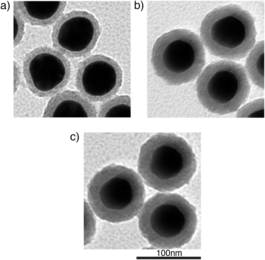 | ||
| Fig. 2 TEM images of Au@SiO2 core–shell NPs with 53 nm Au cores coated with 10 nm (a), 17 nm (b) and 21 nm (c) average silica shells. | ||
Fig. 3a presents the emission of the F8BT/MEH-PPV thin films for different concentrations of Au@SiO2 (53:10) core–shell NPs, based on excitation pump pulse energies. For a thin waveguide without NPs (blue color), the emission increased at a low rate by increasing the pump pulse energy, until it reached the threshold value of 1.75 μJ cm−2 × 10², and from there the ASE increased with a higher rate. The appearance of ASE is due to the waveguide confinement in a high refractive index polymer thin film. As shown in Fig. 3a, addition of Au@SiO2 NPs decreases the threshold while increasing the slope efficiency of ASE. For instance, by adding 10 μL of 8 mM Au@SiO2 (53:10) NPs (black dots), the threshold reduced down to 0.65 μJ cm−2 × 10², and the slope efficiency increased. However, for intense pumping above 2 μJ cm−2 × 10², the slope efficiency was changed due to the reduction of the refractive index and formation of triplet energy transfer.21 This was accompanied by an increase in the FWHM and a blue shift of the emission. The threshold and slope efficiency are a function of the number of particles, thus the addition of NPs up to 80 μL reduced the threshold down to 0.35 μJ cm−2 × 10² and increased the slope efficiency, but no sharp spikes were observed. Quantum yield (QY) measurements revealed that it increased with the number of particles. For 80 μL, the QY reached the value of 0.128, from 0.106 for the undoped case. Fig. 3b shows the ratio of emission intensity for Au@SiO2 NP-doped thin films as compared to the undoped thin film, based on pump pulse energies, regardless of the nature of emission. For 10 μL of Au@SiO2 NPs, this ratio was initially increased by increasing the pump pulse energy, and reached a maximum of 50 times at 1.25 μJ cm−2 × 10². This enhancement was expected because, according to Fig. 3a, for the undoped thin film the threshold is around 1.75 μJ cm−2 × 10² and the emission intensity increases at a low rate, while for the thin film doped with 10 μL of NPs the threshold is around 0.65 μJ cm−2 × 10² and the intensity grows at a higher rate. By passing 1.25 μJ cm−2 × 10² the ratio starts to decrease at a low rate until reaching 1.75 μJ cm−2 × 10², the threshold for the undoped thin film. For pump pulse energies beyond 1.75 μJ cm−2 × 10² the enhancement ratio decreases at a higher rate, revealing different dynamics induced by triplet energy transfer. Higher ratios were achieved for higher concentrations of the doping NPs. For ratios under 1.25 μJ cm−2 × 10², the enhancement rate was increased by increasing the concentration, while for ratios beyond 1.25 μJ cm−2 × 10² the reduction rate was increased. The maximum enhancement, as large as 200 times, was observed for the thin film doped with 80 μL of NPs. In this experiment, Au@SiO2 NPs, as nanoscale antennas, strongly scatter the emission of the gain medium and consequently enhance the ASE because of their role in increasing the optical path and confinement of emitted light by multiple scattering and reflection in the thin film waveguide.
 | ||
| Fig. 3 Emission of the F8BT/MEH-PPV thin film waveguides for different concentrations of Au@SiO2 NPs (53:10) when they were excited resonantly with different pump pulse energies. (a) Emission of the F8BT/MEH-PPV thin film based on excitation pump pulse energies for undoped thin film, and thin film doped with 10, 20, 40 and 80 μL of 8 mM Au@SiO2 (53:10) core–shell NPs when they are excited resonantly. (b) Ratio of emission for thin films doped with different concentrations of Au@SiO2 core–shell NPs to undoped film based on excitation pump pulse energies. | ||
By increasing the concentration of Au@SiO2 NPs, they eventually shaped a feedback mechanism due to plasmonic scattering and confinement, which is further supported by total internal reflection.
Fig. 4a demonstrates typical coherent nanoplasmonic random lasing (red line) when 200 μL of Au@SiO2 (53:10) core–shell NPs was loaded in the semiconductor polymer matrix, as compared with the output signal for excitation below the lasing threshold (black line). Multiple lasing spikes with FWHM less than 0.1 nm, associated with different modes of the random laser, were shaped as a result of the interference of waves in the organic semiconductor thin film. Fig. 4b illustrates the surface profile of the plasmonic random laser, each large peak representing a single NP. Based on these peaks, the average distance was calculated to be shorter than 280 nm. The corresponding characteristics diagram (red line) is shown in Fig. 4c. In this figure, the laser slope efficiency of the plasmonically nano-engineered random laser, using 53 nm Au NP cores coated with 10 nm silica shell (red), is compared with slope efficiencies of Au NPs coated with 17 nm (orange) and 21 nm (black) silica shells, in order to demonstrate that it is possible to tune the energy coupling between the plasmonic nano-antennas and excitons in the organic semiconductor thin film. The slope efficiency was increased by two times, by reducing the silica shell thickness from 21 nm to 10 nm, while there is a minor change in the threshold. Therefore, despite the earlier investigations in a bulk of dye solution,22 it was observed that in a thin film of organic semiconductor the silica shell dominantly influences the stimulated emission by increasing the slope efficiency, rather than reducing the lasing threshold. Here, the enhanced electric field in the vicinity of NPs can increase the excitation and/or radiative decay rate of the gain medium, however, the QY values show a minor contribution of the radiative decay rate in the enhanced emission. FDTD simulations were carried out for Au@SiO2 (53:10) and Au@SiO2 (53:21), to obtain a better insight into the distribution of the electric field in these resonantly coupled nano-engineered systems.
 | ||
| Fig. 4 (a) Coherent nanoplasmonic random lasing for a thin film of F8BT/MEH-PPV doped with 200 μL of Au@SiO2 core–shell (53:10) NPs (red line) compared with the output signal for excitation below the lasing threshold (black line). (b) Surface profile of the random laser. Large peaks are associated with the Au@SiO2 NPs doped in the waveguide. (c) Laser characteristics diagram and slope efficiency for random lasers doped with Au@SiO2 core–shell NPs with different thicknesses of silica shell. | ||
Nanoplasmonic random lasers can be engineered to work efficiently if the core–shell system is designed to exploit the enhanced and nanoscale electric field. Comparison between Fig. 5a and b shows that for NPs with 10 nm silica shell thickness, a stronger electric field is available outside the silica shell. The excitation rate of the gain medium comprising Au@SiO2 NPs doped in an organic semiconductor polymer matrix is a function of the distance between the NPs and semiconductor polymer, and it decreases by increasing this distance. In fact, the maximum value of the electric field is located on the surface of the NPs, however, because of the high absorption loss due to direct electron transfer, in this case, it quenches the emission of the semiconductor polymer molecules.23,24 Since the change in the QY is not significant, the enhancement of the excitation rate25 in the close vicinity of the NPs is dominantly responsible for the observed behavior in Fig. 4c through providing the highest available localized electric field for the organic semiconductor molecules. This experiment clearly demonstrates that it is possible to plasmonically nano-engineer the function of random lasers in organic semiconductor thin films with a random distribution of plasmonic NPs and a sufficient overlap of plasmonic and organic semiconductor energy levels to form low threshold and efficient random lasers.
 | ||
| Fig. 5 Distribution of the electric field around the Au@SiO2 core–shell NPs based on FDTD simulation when it was excited along the x-direction. (a) Au@SiO2 core–shell NP with a 53 nm Au core diameter and 10 nm shell thickness. (b) Au@SiO2 NP with a 53 nm Au core diameter and 21 nm shell thickness. | ||
Conclusions
In conclusion, we have implemented plasmonically nano-engineered random lasing in a hybrid system of an organic semiconductor thin film and Au@SiO2 core–shell plasmonic sites, using the silica shells to tune the energy coupling. NPs are designed to have their plasmon resonance spectrum overlapping the emission and excitation energy levels of the high refractive index semiconductor polymer waveguide, and provide the required feedback and emission enhancement. It was demonstrated that the efficiency of these coherent random lasers can be controlled by tuning the energy coupling between plasmon and exciton through adjusting the thickness of the insulating silica shells. These nano-engineered plasmonic lasers are simple, small, affordable and easy to make, which makes them promising for biomedical and sensing applications.Experimental section
Random laser fabrication
Poly[2-methoxy-5-(2-ethylhexyloxy)-1,4-phenylene-vinylene] (F8BT) and poly[(9,9-dioctylfluorenyl-2,7-diyl)-alt-co-(1,4-benzo-{2,1′,3}-thiadiazole)] (MEH-PPV) were purchased from ADSDYES and used as received. 37 mg of F8BT (30 mg)/MEH-PPV (7 mg) was dissolved in 1 mL of toluene and incubated for 24 h at room temperature for complete dissolution, and then stirred for a few seconds. 8 mM Au@SiO2 core–shell NPs in toluene were synthesized as previously described.26 Au@SiO2 NPs were mixed with 200 μL of the semiconductor polymer solution and diluted up to 400 μL. The solution was spin-coated onto glass substrates using a Laurel WS-400B-6TFM/LITE/3AS spin-coater to form 300 nm thin films. Thin films were dried on a hot plate for 1 min at 110 °C to remove the remaining solvent. A NT-MDT MOD-1M plus scanning probe microscope (SPM) was used for surface characterization, a Dektak 0815 profilometer for thickness measurements, an Elmer Lamda 2 UV-vis spectrometer for measurement of extinction spectra, a Hamamatsu C9920-02 for QY measurements, a Soliton PNG-M02010 frequency-doubled diode pumped Nd:YAG laser with a pulse length of 300 ps for optical excitation, a Horiba iHR200 spectrometer equipped with Synapse's thermoelectric cooled CCD for recording emission spectra and a Coherent LabMax-Top for measuring the energy of the laser.Acknowledgements
The research leading to these results has received funding from the European Commission, Marie Curie Initial Training Network (ITN) “Dendreamers” FP7 215884, and the European Union Seventh Framework Programme under Grant Agreement No. 262348 (ESMI).References
- A. Wokaun, H. P. Lutz, A. P. King, U. P. Wild and R. R. Ernst, J. Chem. Phys., 1983, 79, 509 CrossRef CAS.
- S. A. Maier, M. L. Brongersma, P. G. Kik, S. Meltzer, A. A. G. Requicha and H. A. Atwater, Adv. Mater., 2001, 13, 1501 CrossRef CAS.
- P. Muhlschlegel, H. J. Eisler, O. J. F. Martin, B. Hecht and D. W. Pohl, Science, 2005, 308, 1607 CrossRef CAS PubMed.
- M. A. Noginov, G. Zhu, A. M. Belgrave, R. Bakker, V. M. Shalaev, E. E. Narimanov, S. Stout, E. Herz, T. Suteewong and U. Wiesner, Nature, 2009, 460, 1110 CrossRef CAS PubMed.
- S. Gottardo, R. Sapienza, P. D. García, A. Blanco, D. S. Wiersma and C. López, Nat. Photonics, 2008, 2, 429 CrossRef CAS.
- G. D. Dice, S. Mujumdar and A. Y. Elezzabi, Appl. Phys. Lett., 2005, 86, 131105 CrossRef.
- R. C. Polson and Z. V. Vardeny, Appl. Phys. Lett., 2004, 85, 1289 CrossRef CAS.
- B. Redding, M. A. Choma and H. Cao, Nat. Photonics, 2012, 6, 355 CrossRef CAS PubMed.
- W. Z. W. Ismail, G. Liu, K. Zhang, E. M. Goldys and J. M. Dawes, Opt. Express, 2016, 24, A85 CrossRef CAS PubMed.
- Z. Wang, X. Meng, S. H. Choi, S. Knitter, Y. L. Kim, H. Cao, V. M. Shalaev and A. Boltasseva, Nano Lett., 2016, 16, 2471 CrossRef CAS PubMed.
- X. Meng, K. Fujita, Y. Zong, S. Murai and K. Tanaka, Appl. Phys. Lett., 2008, 92, 201112 CrossRef.
- O. Popov, A. Zilbershtein and D. Davidov, Appl. Phys. Lett., 2006, 89, 191116 CrossRef.
- T. Zhai, X. Zhang, Z. Pang, X. Su, H. Liu, S. Feng and L. Wang, Nano Lett., 2011, 11, 4295 CrossRef CAS PubMed.
- T. Zhai, Z. Xu, X. Wu, Y. Wang, F. Liu and X. Zhang, Opt. Express, 2016, 24, 437 CrossRef CAS PubMed.
- L. Novotny and P. Bharadwaj, Opt. Express, 2007, 15, 14266 CrossRef.
- Y. Chen, K. Munechika and D. S. Ginger, Nano Lett., 2007, 7, 690 CrossRef CAS PubMed.
- S. Gerber, F. Reil, U. Hohenester, T. Schlagenhaufen, J. R. Krenn and A. Leitner, Phys. Rev. B: Condens. Matter Mater. Phys., 2007, 75, 073404 CrossRef.
- K. L. Kelly, E. Coronado, L. L. Zhao and G. C. Schatz, J. Phys. Chem. B, 2003, 107, 668 CrossRef CAS.
- J. Ziegler, C. Wörister, C. Vidal, C. Hrelescu and T. A. Klar, ACS Photonics, 2016, 3, 919 CrossRef CAS PubMed.
- T. Zhai, J. Chen, L. Chen, J. Wang, L. Wang, D. Liu, S. Li, H. Liu and X. Zhang, Nanoscale, 2015, 7, 2235 RSC.
- Z. V. Vardeny, Ultrafast Dynamics and Laser Action of Organic Semiconductors, CRC Press, 2009 Search PubMed.
- X. Meng, K. Fujita, S. Murai, T. Matoba and K. Tanaka, Nano Lett., 2011, 11, 1374 CrossRef CAS PubMed.
- V. Walhorn, J. Paskarbeit, H. G. Frey, A. Harder and D. Anselmetti, Beilstein J. Nanotechnol., 2011, 2, 645 CrossRef CAS PubMed.
- Z. Gueroui and A. Libchaber, Phys. Rev. Lett., 2004, 93, 166108 CrossRef PubMed.
- J. A. Schuller, E. S. Barnard, W. Cai, Y. C. Jun, J. S. White and M. L. Brongersma, Nat. Mater., 2010, 9, 193 CrossRef CAS PubMed.
- I. Pastoriza-Santos, J. Perez-Juste and L. M. Liz-Marzán, Chem. Mater., 2006, 18, 2465 CrossRef CAS.
| This journal is © The Royal Society of Chemistry 2017 |