Uniform and perfectly linear current–voltage characteristics of nitrogen-doped armchair graphene nanoribbons for nanowires†
Lingling
Liu
a,
Xiao-Fei
Li
*a,
Qing
Yan
a,
Qin-Kun
Li
a,
Xiang-Hua
Zhang
a,
Mingsen
Deng
b,
Qi
Qiu
a and
Yi
Luo
bcd
aSchool of Optoelectronic Information, University of Electronic Science and Technology of China, Chengdu, Sichuan 610054, P. R. China
bGuizhou Synergetic Innovation Center of Scientific Big Data for Advanced Manufacturing Technology, Guizhou Education University, Guiyang, 550018, China
cHefei National Laboratory for Physical Science at the Microscale, University of Science and Technology of China, Hefei, Anhui 230026, P. R. China
dDepartment of Theoretical Chemistry and Biology, School of Biotechnology, KTH Royal Institute of Technology, S-10691 Stockholm, Sweden
First published on 29th November 2016
Abstract
Metallic nanowires with desired properties for molecular integrated circuits (MICs) are especially significant in molectronics, but preparing such wires at a molecular level still remains challenging. Here, we propose, from first principles calculations, experimentally realizable edge-nitrogen-doped graphene nanoribbons (N-GNRs) as promising candidates for nanowires. Our results show that edge N-doping has distinct effects on the electronic structures and transport properties of the armchair GNRs and zigzag GNRs (AGNRs, ZGNRs), due to the formation of pyridazine and pyrazole rings at the edges. The pyridazine rings raise the Fermi level and introduce delocalized energy bands near the Fermi level, resulting in a highly enhanced conductance in N-AGNRs at the stable nonmagnetic ground state. Especially for the family of AGNRs with widths of n = 3p + 2, their semiconducting characteristics are transformed to metallic characteristics via N-doping, and they exhibit perfectly linear current–voltage (I–V) behaviors. Such uniform and excellent features indicate bright application prospects of the N-AGNRs as nanowires and electrodes in molectronics.
Introduction
Graphene nanoribbon (GNR) is a fantastic type of one-dimensional material with novel properties that are distinct from graphene.1–3 GNRs in different configurations are appealing in terms of their electronic properties that are governed by chirality and width.4,5 Chiral and zigzag GNRs (CGNRs, ZGNRs) are spin-polarized with appealing magnetic structures, whereas armchair GNRs (AGNRs) are spin-unpolarized and can be classified into three different families due to their distinct width-dependent energy gaps. For practical device applications, the widths of the GNRs should be several nanometers or even reach molecular scale levels.4–6 Ultra-narrow GNRs (sub-10 nm) with precise edge structures have already been synthesized in experiments by the unzipping of carbon nanotubes (CNTs),7 the controlled cutting of graphene8 and a chemical bottom-up fabrication,9–12 thus rendering GNR as an attractive alternative for the fabrication of switches,13 transistors,14 filters,2 rectifiers15,16 and other emerging devices.17–20Although the obtained GNRs have flexible one-dimensional (1D) structures, they normally cannot be used directly as nanowires in molecular integrated circuits (MICs), due to the fact that their semiconducting and nonlinear current–voltage (I–V) characteristics can result in non-trivial changes to the functions of integrated devices.21 Metal materials are widely proposed and adopted as electrodes in molectronics for obvious reasons,22 but to obtain molecular-scale metal nanowires with desired properties for MICs remains a huge challenge. CNTs have also been presented as electrodes in molectronics,15,16,23,24 due to the fact that CNTs possess 1D structures and metallic properties that can be obtained by controlling their chiralities during fabrication. Although metallic CNTs are proposed as nanowires in MICs, they look to be not the most desired candidates, due to their tubular structures making the crossed-connections in MICs difficult to utilize. In contrast, GNRs have perfect planar structures and can tightly adhere to molecular devices by the formation of covalent bonds. Therefore, for the adequate use of nanowires in MICs, it is essential to design and fabricate metallic GNRs with desirable properties.21
Chemical doping is a promising route to tailor the properties of graphene materials.17 In particular, substitutional nitrogen-doping (N-doping),25,26 which prefers to occur at the edges and vacancies of graphene,27 has an impressive ability to enhance the performance of graphene materials in multiple important applications. For example, N-doping can induce robust negative differential resistance (NDR) behaviour amid other useful effects in GNRs,18–20 and the obtained N-graphene exhibits strong catalytic capacity in oxygen reduction,28,29 hydrogen evolution30 and nitrogen fixation.31
In this work, we propose from first principles calculations that fully edge N-doped AGNRs (N-AGNRs), which have been synthesized in recent experiments,32 can be used in nanowire applications in MICs, due to the fact that they are observed to possess unique metallic electronic structures with perfectly linear I–V characteristics.
Models and methods
Both ZGNRs and AGNRs, and the N-doping that occurred at the single and double-edges of the ribbons, were evaluated. The width-dependent band gaps4,5 of the AGNRs with various widths (n = 5, 8–17) were explored. To eliminate the artificial periodic interactions, a vacuum distance of 15 Å along the x and y directions was used.All the calculations were performed using SIESTA 3.2,33 by employing spin-resolved density functional theory (DFT) in combination with non-equilibrium Green’s functions (NEGF). The Perdew–Burke–Ernzerhof (PBE)34 generalized gradient approximation (GGA) was used for the exchange correction, and a numerical double-ζ plus polarization (DZP) basis set was used with an energy shift of 0.01 Ry to determine the cutoff radii of the atomic orbitals. The Brillouin zone (BZ) was sampled with a Monkhorst–Pack grid of 1 × 1 × 23 in the structural optimizations and band-structure analyses, and a grid of 1 × 1 × 100 in the transport calculations. All the structures were fully relaxed until the residual force on each atom was smaller than 0.001 eV Å−1.
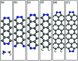
As a representative example, the optimized structures of the double-edge N-AGNRs with n = 9, 10 and 11 and the single-edge N-AGNR with n = 11, as well as the single and double-edge N-ZGNRs with a width of n = 8, are displayed in Fig. 1(a)–(f). One can see that the N-doping forms five-membered pyrazole and six-membered pyridazine rings at the zigzag and armchair edges, respectively. The calculated binding energies of the pyrazole and pyridazine rings have been reported32 to be −2.50 eV per N2 and −1.96 eV per N2 respectively, suggesting relative stabilities and quite different effects on the electronic structures and transport properties of the ZGNRs and AGNRs.
The current was evaluated using the Landauer–Büttiker formalism
Results and discussion
Electronic structures
It is well-known that the ground states of AGNRs and ZGNRs are nonmagnetic (NM) and anti-ferromagnetic (AFM) states, respectively. We first considered the N-doping effect on the electronic structure. Our calculations showed that the energy differences (ΔE) between the ferromagnetic (FM) and NM states of single- and double-edge N-AGNRs are very small (<0.01 eV), yet AFM states never appear. This means that N-doping cannot change the ground state of AGNRs. The quantum confinement in AGNRs greatly restrains the emergence of spin-polarization.12For double-edge N-ZGNRs, the ΔE between the AFM and NM states, and between the AFM and FM states is also very small (<0.01 eV), indicating that the two magnetic edge states of the ZGNRs are totally destroyed by the edge N-doping that results in NM ground states. In contrast, for single-edge N-ZGNR, the ΔE between the FM and NM states is about 0.14 eV and the spin moment for the FM state is about 0.66 μB. It is obvious that the magnetic edge state remains at the undoped edge, which makes the FM state be the ground state of the system.4,5,12
Therefore, both the double-edge N-AGNR and N-ZGNR always possess NM ground states, indicating a significant advantage in nanowire applications.
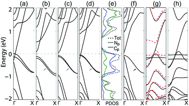
To further understand this advantage, the band structures of the double-edge N-AGNRs with n = 8, 9, 10 and 11 at the NM ground state are shown in Fig. 2. One can see that N-doping introduces two delocalized impurity-bands (as denoted by the blue short arrows) in each system. The bands approach each other as the width (n) increases, due to the gradually decreased quantum confinement in the AGNRs. Introducing delocalized bands near the Fermi level by doping is a hot topic in modern science and technology, due to its dramatic ability to tune the properties of host materials. More importantly, the ribbons with widths of n = 8 and 11 exhibit bands which cross the Fermi level, indicating metallic characteristics. It is obvious that the band that crosses the Fermi level should be the lowest conduction band (CB) of the pristine ribbons. Fig. S1 (in ESI†) shows that the ribbons with n = 14, and 17 also possess such a band running across the Fermi level. Undoubtedly, double-edge N-doping can alternate the electronic properties of all the AGNRs in the family with widths of n = 3p + 2 from semiconducting to metallic, by inducing the CB to run across the Fermi level. This can be well understood by observing the following two facts: that the family of n = 3p + 2 has the narrowest band gap which contrasts with the families of n = 3p and 3p + 1 with the same p,4,5 and that N-doping that occurs at either the edge or the middle of the AGNRs can induce the raising of the Fermi level.20 The combination of these two facts results in the CB crossing the Fermi level, thus resulting in the metallic characteristics.
To further understand the band across the Fermi level, we calculated the normalized partial density of states (PDOS) of the double-edge N-AGNR (n = 11). Considering that the s electrons of N and C atoms are mainly distributed far away from the Fermi level, only the p electrons are depicted in Fig. 2(e). One can see the heavy PDOSs extending and running across the Fermi level, indicating metallic characteristics with a very good electronic conductive ability. Furthermore, it also shows that the total PDOS near the Fermi level solely derives from the interaction between the N-dopants and the pristine AGNR, about 1/3 from the N atoms and 2/3 from the C atoms, thus unambiguously explaining the formation of a delocalized π system. From the point of view of chemistry, besides the formation of two σ bands in the six-membered pyridazine ring, the N atom possesses a lone electron pair, thus a 2p electron remains which forms a π bond with the neighbouring atoms. This characteristic is similar to that of the –CH– group at the armchair edges as shown in the inset of Fig. 1(a).
We also considered N-doping that occurs at a single edge of the AGNR and, as an example, the band structure of single-edge N-AGNR with n = 11 is plotted in Fig. 2(f). One can see that although a well-delocalized band (denoted by a black arrow) is present near the Fermi level, the system is still semiconducting with a small band gap of 0.08 eV. This is because a delocalized π bond can only be formed by single-edge N-doping and the Fermi level is not raised enough to close the band gap, even if the reduction of the band gap is obvious.
Different from the N-AGNRs, localized impurity-bands emerge near the Fermi level of both the single-edge and double-edge N-ZGNRs, as shown in Fig. 2(g) and (h). We noticed that the N atoms at the armchair edges are located in the six-membered pyridazine rings, which is favourable to form delocalized π bonds, whereas the N atoms at the zigzag edges comprise part of the five-membered pyrazole rings, which prefer to form localized bonds. Therefore, this is the structural reason that explains the formation of delocalized and localized bonds in N-AGNRs and N-ZGNRs, respectively.
For the single-edge N-ZGNR, N-doping introduces only one localized band near the Fermi level and thus eliminates only one edge state of the pristine ZGNR, resulting in the FM ground state. Hence, the system is still spin-dependent and a band largely splits, as shown in Fig. 2(g). Undoubtedly, the split band is the magnetic edge-state from the undoped edge. For the double-edge N-ZGNR, two edge states of the pristine ZGNR are completely eliminated by N-doping, resulting in the NM ground state. One can see that two localized bands are present near the Fermi level of the system, and the lowest CB and the highest valence band (VB) are degenerated across the Fermi level, indicating the spin-independent metallic transport properties of the system.
Electronic transport properties
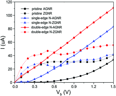
To evaluate the possibility to use metallic N-GNRs as nanowires, we focused on their electronic transport properties. To avoid direct interaction between electrodes, a long section of the ribbons containing 9 unit cells of N-AGNR or 15 unit cells of N-ZGNR was chosen as the central scattering region (CSR) in the transport calculations. The obtained I–V characteristics of the single-edge and double-edge N-AGNRs (n = 11), and the single-edge and double-edge N-ZGNRs, as well as the pristine AGNR and ZGNR at their ground states, are shown in Fig. 3. The currents of the spin-up and spin-down systems in single-edge N-ZGNR and pristine ZGNR are summarized for comparative purposes.For the ZGNRs, one can see that the current starts to flow at zero bias, confirming the metallic characteristics. Moreover, the N-doping enhances the conductance of the system, especially at the low bias region, as suggested in the band structure calculations. Furthermore, their I–V curves are nonlinear, implying inadequate performance for use as nanowires.
In contrast, the situation for the AGNRs is quite different. One can see that the single and double-edge N-doping reduces the threshold voltage from 0.4 V for the pristine AGNR to about 0.2 V and 0.0 V, respectively, confirming the important role of armchair-edge N-doping in reducing the band gap, and transforming the pristine AGNR from semiconducting to metallic characteristics. Moreover, at each bias the current is several times larger than that of pristine AGNR, and the linear increasing voltage is accompanied by a linear increase in current in both the single and double-edge N-AGNRs. The perfectly linear I–V characteristics are desirable and pivotal properties for nanowire applications in molectronics.
Considering that the N-AGNRs with different widths have similar band structures, especially near the Fermi level, as shown in Fig. 2(a) for n = 8, Fig. 2(d) for n = 11, Fig. S1(a) for n = 5, Fig. S1(d) for n = 14 and Fig. S1(h) for n = 17 (ESI†), and that the current of the system at low biases is mainly determined by the bands near the Fermi level, we believe that the linear I–V characteristics observed here for n = 11 should be uniform in the family of n = 3p + 2.
It should be mentioned that middle N-doping in AGNRs can also induce metallic band structures, but it normally results in nonlinear I–V characteristics and even NDR effects.18–20 Other elements and groups have also been proposed as dopants in GNRs, and novel properties with promising applications have been observed.35–40 However, the perfectly linear I–V characteristics revealed here, which is one of the most important features for nanowire applications, have rarely been reported in previous works.
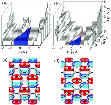
To reveal the underlying mechanisms of linear I–V characteristics, we plotted the contour of the bias-dependent transmission T(E,Vb) of the double-edge N-AGNR and the pristine AGNR in Fig. 4(a) and (b), respectively, in which the bias windows are marked by two red lines, and the meaningful transmissions for the current calculations are coloured in blue.
Clearly, the transmissions from the delocalized impurity-bands (the 45th and 46th orbitals of the N-AGNR cell) are located at the left-side of the bias window. Therefore, they do not contribute to the current. Meanwhile, the transmissions in the bias window have nearly the same intensity of 1. The almost flat feature of the transmissions suggests that edge N-doping does not considerably affect the ballistic transport characteristics of the GNRs. Each electron transports through the N-AGNR nanowire via only one channel, which is afforded by either the 44th or 47th orbitals. Hence, the area under the transmission spectra in the meaningful region increases linearly with increasing voltage, which accounts for the linear I–V characteristics. We plotted the isosurface of the 44th and 47th orbitals in Fig. 4(c) and (d), respectively. One can see that although the two orbitals possess different parities, they are well delocalized and distributed over the entire ribbon, and the N-doping indeed does affect the delocalization. This can be well understood by noticing that some defects can even enhance the transport ability of the GNRs.41 Thus, the orbitals can afford perfect transport channels with unit transmission intensity.
In contrast, for the pristine AGNR, considerable transmissions appear only after the voltage increases to 0.5 V as shown in Fig. 4(b). The first transport channel can be formed only as the CB and VB of the semiconducting system overlap in energy due to the bias increasing. Moreover, the area (coloured) under the transmission spectra extends nonlinearly with increasing voltage, indicating nonlinear I–V characteristics that are undesirable and unsuitable for nanowire applications.
Conclusions
The band structures and transport properties of single-edge and double-edge nitrogen-doped ZGNRs and AGNRs with different widths have been systematically investigated, using a nonequilibrium Green's function formalism in combination with density functional theory. We found that edge N-doping forms five-membered pyrazole rings at the zigzag edges, which destroys the magnetic edge-state, resulting in the FM and NM ground states of the single-edge and double-edge N-doped ZGNRs, respectively. However, in AGNRs, N-doping forms six-membered pyridazine rings, which cannot change the NM ground state, but introduces delocalized bands near the Fermi level, and induces a metallic electronic structure by raising the Fermi level. More importantly, unique and perfectly linear I–V characteristics have been observed for the AGNRs in the family of width n = 3p + 2. The stable NM ground state, the uniformly metallic electronic structure, and the uniform and perfectly linear I–V characteristics indicate promising applications as electrodes and nanowires in molectronics.Acknowledgements
We acknowledge the support from the National Natural Science Foundation of China (Grant No. 61271030, 21643011, 11264005), the Scientific Research Foundation of Hunan Provincial Education Department (15C0329), and the Göran Gustaffson Foundation for Research in Natural Sciences and Medicine.Notes and references
- A. K. Geim and K. S. Novoselov, Nat. Mater., 2007, 6, 183 CrossRef CAS PubMed.
- B. Wang, J. Li, Y. Yu, Y. Wei, J. Wang and H. Guo, Nanoscale, 2016, 8, 3432 RSC.
- J. Huang, R. Xie, W. Wang, Q. Li and J. Yang, Nanoscale, 2016, 8, 609 RSC.
- Y.-W. Son, M. L. Cohen and S. G. Louie, Phys. Rev. Lett., 2006, 97, 216803 CrossRef PubMed.
- M. Y. Han, B. Ozyilmaz, Y. Zhang and P. Kim, Phys. Rev. Lett., 2007, 98, 206805 CrossRef PubMed.
- X. Wang, Y. Ouyang, X. Li, H. Wang, J. Guo and H. Dai, Phys. Rev. Lett., 2008, 100, 206803 CrossRef PubMed.
- L. Y. Jiao, L. Zhang, X. R. Wang, G. Diankov and H. J. Dai, Nature, 2009, 458, 877 CrossRef CAS PubMed.
- L. C. Campos, V. R. Manfrinato, J. D. Sanchez-Yamagishi, J. Kong and P. Jarillo-Herrero, Nano Lett., 2009, 9, 2600 CrossRef CAS PubMed.
- J. Cai, P. Ruffieux, R. Jaafar, M. Bieri, T. Braun, S. Blankenburg, M. Muoth, A. P. Seitsonen, M. Saleh, X. Feng, K. Müllen and R. Fasel, Nature, 2010, 466, 470 CrossRef CAS PubMed.
- H. Suzuki, T. Kaneko, Y. Shibuta, M. Ohno, Y. Maekawa and T. Kato, Nat. Commun., 2016, 7, 11797 CrossRef CAS PubMed.
- Y.-C. Chen, T. Cao, C. Chen, Z. Pedramrazi, D. Haberer, D. G. de Oteyza, F. R. Fischer, S. G. Louie and M. F. Crommie, Nat. Nanotechnol., 2015, 10, 156 CrossRef CAS PubMed.
- P. Ruffieux, S. Wang, B. Yang, C. Sanchez-Sanchez, J. Liu, T. Dienel, L. Talirz, P. Shinde, C. A. Pignedoli, D. Passerone, T. Dumslaff, X. Feng, K. Mullen and R. Fasel, Nature, 2016, 531, 489 CrossRef CAS PubMed.
- F. Xie, Z.-Q. Fan, K. Liu, H.-Y. Wang, J.-H. Yu and K.-Q. Chen, Org. Electron., 2015, 27, 41 CrossRef CAS.
- J. A. Mol, C. S. Lau, W. J. M. Lewis, H. Sadeghi, C. Roche, A. Cnossen, J. H. Warner, C. J. Lambert, H. L. Anderson and G. A. D. Briggs, Nanoscale, 2015, 7, 13181 RSC.
- D. Wei, L. Xie, K. K. Lee, Z. Hu, S. Tan, W. Chen, C. H. Sow, K. Chen, Y. Liu and A. T. S. Wee, Nat. Commun., 2013, 4, 1374 CrossRef PubMed.
- X.-H. Zhang, X.-F. Li, L.-L. Wang, L. Xu and K.-W. Luo, Appl. Phys. Lett., 2014, 104, 103107 CrossRef.
- R. Konnerth, C. Cervetti, A. Narita, X. Feng, K. Mullen, A. Hoyer, M. Burghard, K. Kern, M. Dressel and L. Bogani, Nanoscale, 2015, 7, 12807 RSC.
- H. Ren, Q.-X. Li, Y. Luo and J. Yang, Appl. Phys. Lett., 2009, 94, 173110 CrossRef.
- J. Huang, W. Wang, Q. Li and J. Yang, J. Chem. Phys., 2014, 140, 164703 CrossRef PubMed.
- X.-F. Li, K.-Y. Lian, Q. Qiu and Y. Luo, Nanoscale, 2015, 7, 4156 RSC.
- A. Kimouche, M. M. Ervasti, R. Drost, S. Halonen, A. Harju, P. M. Joensuu, J. Sainio and P. Liljeroth, Nat. Commun., 2015, 6, 10177 CrossRef CAS PubMed.
- A. Bonifas and R. McCreery, Nat. Nanotechnol., 2010, 5, 612 CrossRef CAS PubMed.
- R. H. Baughman, A. A. Zakhidov and W. A. de Heer, Science, 2002, 297, 787 CrossRef CAS PubMed.
- X. Guo, A. A. Gorodetsky, J. Hone, J. K. Barton and C. Nuckolls, Nat. Nanotechnol., 2008, 3, 163 CrossRef CAS PubMed.
- D. Wei, Y. Liu, Y. Wang, H. Zhang, L. Huang and G. Yu, Nano Lett., 2009, 9, 1752 CrossRef CAS PubMed.
- X. Wang, X. Li, L. Zhang, Y. Yoon, P. K. Weber, H. Wang, J. Guo and H. Dai, Science, 2009, 324, 768 CrossRef CAS PubMed.
- X.-F. Li, K.-Y. Lian, L. Liu, Y. Wu, Q. Qiu, J. Jiang, M. Deng and Y. Luo, Sci. Rep., 2016, 6, 23495 CrossRef CAS PubMed.
- H. J. Cui, H. M. Yu, J. F. Zheng, Z. J. Wang, Y. Y. Zhu, S. P. Jia, J. Jia and Z. P. Zhu, Nanoscale, 2016, 8, 2795 RSC.
- D. Guo, R. Shibuya, C. Akiba, S. Saji, T. Kondo and J. Nakamura, Science, 2016, 351, 361 CrossRef CAS PubMed.
- Y. Zheng, Y. Jiao, Y. Zhu, L. H. Li, Y. Han, Y. Chen, A. Du, M. Jaroniec and S. Z. Qiao, Nat. Commun., 2014, 5, 3783 Search PubMed.
- X.-F. Li, Q.-K. Li, J. Cheng, L. Liu, Q. Yan, Y. Wu, X.-H. Zhang, Z.-Y. Wang, Q. Qiu and Y. Luo, J. Am. Chem. Soc., 2016, 138, 8706 CrossRef CAS PubMed.
- I.-Y. Jeon, H.-J. Choi, M. J. Ju, I. T. Choi, K. Lim, J. Ko, H. K. Kim, J. C. Kim, J.-J. Lee, D. Shin, S.-M. Jung, J.-M. Seo, M.-J. Kim, N. Park, L. Dai and J.-B. Baek, Sci. Rep., 2013, 3, 2260 Search PubMed.
- J. M. Soler, E. Artacho, J. D. Gale, A. García, J. Junquera, P. Ordejón and D. Sánchez-Portal, J. Phys.: Condens. Matter, 2002, 14, 2745 CrossRef CAS.
- J. P. Perdew, K. Burke and M. Ernzerhof, Phys. Rev. Lett., 1996, 77, 3865 CrossRef CAS PubMed.
- X.-F. Yang, W.-Q. Zhou, X.-K. Hong, Y.-S. Liu, X.-F. Wang and J.-F. Feng, J. Chem. Phys., 2015, 142, 024706 CrossRef PubMed.
- Q. Yan, B. Huang, J. Yu, F. Zheng, J. Zang, J. Wu, B.-L. Gu, F. Liu and W. Duan, Nano Lett., 2007, 7, 1469 CrossRef CAS PubMed.
- M. Wu, X. Wu and X. C. Zeng, J. Phys. Chem. C, 2010, 114, 3937 CAS.
- E. J. Kan, Z. Li, J. Yang and J. G. Hou, J. Am. Chem. Soc., 2008, 130, 4224 CrossRef CAS PubMed.
- S. Dutta, A. K. Manna and S. K. Pati, Phys. Rev. Lett., 2009, 102, 096601 CrossRef PubMed.
- C. Bronner, S. Stremlau, M. Gille, F. Braube, A. Haase, H. Stefan and T. Petra, Angew. Chem., Int. Ed., 2013, 52, 4422 CrossRef CAS PubMed.
- X.-H. Zhang, X.-F. Li and Q. Qiu, J. Appl. Phys., 2016, 120, 164303 CrossRef.
Footnote |
| † Electronic supplementary information (ESI) available. See DOI: 10.1039/c6cp06640b |
| This journal is © the Owner Societies 2017 |


