Band-structure engineering in conjugated 2D polymers†
Received
3rd September 2016
, Accepted 28th September 2016
First published on 28th September 2016
Abstract
Conjugated polymers find widespread application in (opto)electronic devices, sensing, and as catalysts. Their common one-dimensional structure can be extended into the second dimension to create conjugated planar sheets of covalently linked molecules. Extending π-conjugation into the second dimension unlocks a new class of semiconductive polymers which as a consequence of their unique electronic properties can find usability in numerous applications. In this article the theoretical band structures of a set of conjugated 2D polymers are compared and information on the important characteristics band gap and valence/conduction band dispersion is extracted. The great variance in these characteristics within the investigated set suggests 2D polymers as exciting materials in which band-structure engineering can be used to tailor sheet-like organic materials with desired electronic properties.
1 Introduction
Synthetic organic two-dimensional polymers (2DP) can be envisioned as intermediate materials between layered covalent organic frameworks (COF) and inorganic 2D materials such as graphene, single-layer MoS2, silicene, etc.1 Whereas COF2–4 and microporous conjugated polymer5,6 synthesis is a mature research field and tailored materials with desired properties are reported with increasing frequency,7–9 the fabrication of single sheets of covalently linked organic building blocks remains a great technical challenge. Two major synthetic routes towards conjugated and non-conjugated 2DPs are currently pursued, one using solid-state topochemical reactions,10 the other making use of surface-mediated reactions in ultra-high vacuum.11–15 Solution-based approaches emerged as an alternative reaction pathway and are currently widely explored.16–19 Delamination of layered 2D COFs offers a viable alternative to afford 2DPs10,20–22 directly from the parent material.
Much of the research of organic 2D materials is driven by their expected unique electronic properties. Theoretical studies predict 2DPs as semiconductors with tuneable band gap and correlate geometric structure with electronic properties.23–29 In parallel, graphene allotropes have been studied intensively which conductive properties vary widely from insulators to metals including numerous semiconductors.30 These include, for example, graphynes and graphdyines,31 biphenylene sheets,32–35 phagraphene,36 or T-graphene.37 Band-structure engineering in two dimensions emerges from these studies as an achievable goal and inspiration can be drawn from studies of COFs that start to reach out towards their characterization for applications in (opto)electronic devices, solar cells, etc.
For example, photoconductive properties of a pyrene based COF have recently been reported with long-range exciton delocalization.38 Phthalocyanine- and porphyrin-based COFs have shown charge carrier mobilites up to several cm2 V−1 s−1.39,40 Donor–acceptor properties within the same COF were reported,41,42 as well as first results on a photovoltaic device.43,44 Several COFs have been shown to be catalytically active, which can be traced back to the electronic structure and chemical composition of the frameworks.45,46 However, for strictly two-dimensional layers there are still very few studies in which any physical or chemical property is reported, although the great number of studies on the properties of COFs clearly encourages research in this direction. Few experimental examples confirm the reduction of the band gap in the transition from molecular precursor to 2DP,47,48 which is predicted to be a general feature of conjugated 2DPs.29 The HOMO/LUMO gap decreases continuously with increasing polymer size until electronic bands are formed in the ideal infinite 2DP. In order to gain deeper insight into the electronic band structure of extended conjugated materials, systematic density functional theory calculations on different experimentally realized 2D polymers were performed. The focus rests on free-standing 2DPs with extended π-conjugation in the plane of the polymer. Parameters that alter the band structure are discussed in detail such as the effect of chemical composition of the molecular repeat unit (unit cell), dihedral angles between different π-electron systems within one polymer, configurational isomerization, and the change in band structure in the transition from monolayer to multilayer and to 2D COF. The results unveil the wealth of electronic structures that can be realized in 2DPs with tuneable properties like the band gap and valence/conduction band dispersion.
2 Results and discussion
2.1 Conjugation length in repeat unit
Special attention has drawn a 2DP dubbed porous graphene (1), which was synthesized using metal substrates as templates.49,50 The electronic structure was reported previously with direct band gaps of 2.34 eV (LDA),51,52 2.40 eV (PW91),53 2.48 eV (PW91),54 3.2 eV (HSE06)51 and 3.91 eV (B3LYP),29 of which the HSE06 and B3LYP values are probably the best approximations to the still unreported experimental value. This is a consequence of a cancellation of inadequacies to describe the band gap of the two contributions to hybrid functionals, the Hartree–Fock contribution, which overestimates band gaps, and the underestimation through pure DFT. The here calculated PBE value of 2.42 eV is lower than the HSE06 and B3LYP values as the PBE functional underestimates band gaps compared to the hybrid functionals. However, the band structures qualitatively agree with relatively large valence and conduction band dispersion (Fig. 1a). Despite being cross-conjugated,551 allows efficient charge delocalization over the polymer, and hence a finite effective mass of charge carriers (see later discussion).
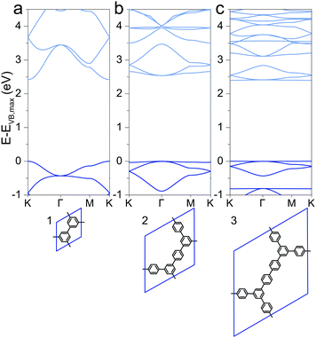 |
| | Fig. 1 Band structures of (a) 1, (b) 2, and (c) 3. The energy of the valence band maximum VB,max is set to 0. | |
Extending the ring size in porous graphene by introducing additional phenyl rings results in a series of isoreticular networks 1, 2, and 3. Like 1, the two structures in Fig. 1b and c have been experimentally realized as monolayers on metal substrates.56–58 For better comparison, 2DPs were calculated with coplanar phenyl groups – the effect of dihedral twists is discussed below. The band gap remains almost constant with increasing number of phenyls and thus increasing spatial extension between vertices (2.54 eV for 2 and 2.40 eV for 3). Two competing factors are responsible for the constant band gap, one is the more pronounced effect of cross-conjugation, which increases the gap, and the other factor being the longer direct conjugation pathway between cross-conjugated vertices, which reduces the gap. Concurrently, conduction and valence bands become flatter with increasing number of phenyl rings. Flat bands are also reported for structurally similar and fully planar 1,3,5 graphdiyne.15 The reduced band gap in structure 3 compared to 2 is in agreement with previously calculations with similar 2DPs including triazine and boroxine groups at the vertices.24 The effect of heteroatom substitution can be studied on 2DP 2. Substituting carbon by nitrogen and converting the vertex phenyls into s-triazines transforms 2 into a single sheet of the conjugated microporous polymer CTF-1 (4, Fig. 2a).5 In a similar fashion, replacing the vertex phenyls by boroxine converts 2 into the covalent organic framework COF-1 (5, Fig. 2c).2,16,59 The band gap increases in the series 2, 4, 5 because of the decreasing electron conjugation in the heterocycles (2.54 eV, 2.66 eV, and 3.59 eV, respectively). Structure 4 has a slight indirect gap between K and Γ, the direct gap at Γ is 2.70 eV. At the same time, band dispersion decreases from 2 to 4 and 5. This has prominent consequences for the synthesis of conductive materials like COFs, in which triazine and boroxine rings are commonly formed as linking units in their synthesis. In-plane conjugation is suppressed compared to phenyl rings, which adds to the deteriorating effect of cross-conjugation at the vertexes and leads to suppressed charge carrier mobility along the plane.
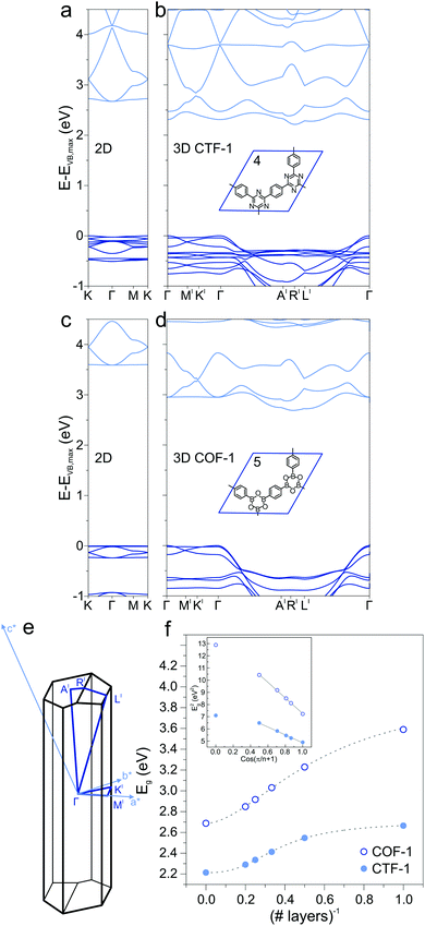 |
| | Fig. 2 (a) Band structure of a single layer of CTF-1 4 and (b) of the crystal of CTF-1. (c) Band structure of a single layer of COF-1 5 and (d) of the crystal of COF-1. (e) Brillouin zone of the 3D crystal structure of CTF-1 and COF-1. (f) Dependence of the band gap Eg on number of layers for 4 and 5. The inset shows the linear correlation between the squares of Eg and cos(π/(n + 1)), where n is the number of layers. | |
2.2 2D, multilayers, and 3D
In the transition from strictly two-dimensional polymer to layered COF, additional band-gap reduction is achieved. CTF-1 4 and COF-1 5 were investigated as model systems to study the dependence of the electronic structure on the number of 2DP sheets. The band structures of a single layer (Fig. 2a and c), bilayer, up to five layers, and finally the 3D structure (Fig. 2b and d) were calculated and the band gaps as a function of number of layers is plotted in Fig. 2f. A slip in adjacent layers from the on-top position between adjacent layers is the energetically most favorable structure of CTF-1 and COF-1 and consequently leads to an out-of-plane unit cell vector that is not perpendicular to the a and b vectors spanning the unit cell of the single layer. The Brillouin zone is depicted in Fig. 2e. With increasing number of layers, the band gap decreases due to the interaction with neighboring layers, confirming previous calculations on CTF-1.60 This is reminiscent of the decreased HOMO/LUMO gap in organic semiconductors in the crystalline state compared to the isolated molecule and stems from a destabilization of the occupied electronic state and a stabilization of the unoccupied electronic state.61 The inset of Fig. 2e shows the squares of the band gap as a function of cos(π/(n + 1)) and a linear fit, modeling the sheets as coupled oscillators.62 The smallest gap is found for the 3D structure, which notably shows an indirect band gap (Fig. 2b and c). A similar observation was made for the inorganic semiconductor MoS2, in which a direct gap is found in the single layer and indirect gaps in the multilayer and crystal.63 The rather flat valence and conduction bands of the single layer CTF-1 and COF-1, evidence of localized states and large effective masses of the charge carriers, acquire significant dispersion in 3D. The dispersion is not observed along the symmetry lines in-plane, but perpendicular to the 2DP sheets (from Γ to A′ and L′). The band curvature along these lines leads to smaller effective masses and more efficient charge transport perpendicular to the polymer planes than it is in plane. The π–π stacking between sheets results in better electronic coupling between the sheets than the covalent bonds through the cross-conjugated vertices. This observation is in accord with experimental findings that report enhanced charge transport perpendicular to the 2D sheets in COFs.41,42,64
2.3 Dihedral angle
Another parameter that can be used to adjust the band structure is the dihedral angle of conjugated groups within the plane. The phenyl rings in 2DPs based on tetraphenylporphyrins 6, a building block which can be encountered in surface-confined synthesis of 2DPs 6,65,66 in 2D COFs,40,64 and in microporous polymers,67 are rotated out of plane with respect to the porphyrin. Steric repulsion between the ortho-hydrogens makes it energetically challenging for the phenyls to lie coplanar to the macrocycle. The crystal structure of tetraphenylporphyrin shows dihedral angles larger 60°,68 whereas the adsorption on solid surfaces reduces the angle considerably to roughly 30°.69 Embedded in COFs, the angle is calculated to be around 45°.64 The environment of the phenylporphyrins thus has a pronounced effect on the dihedral angle and consequently on the electronic structure of the polymer. The valence and conduction bands of 6 are depicted in Fig. 3a as a function of dihedral angle (C2 symmetry in the repeat unit), showing an increasing band gap with increasing angle. Qualitatively, the band structure of 6 resembles the band structures reported previously using the tight-binding crystal orbital method for similar porphyrin-based 2DPs.70 Likewise, the central phenyl ring between two vertex rings of 2 can rotate out of the plane, and in fact does so in the energetically favorable geometry. The valence band (dotted line) and the next lower band (solid line), which meet at the Γ point, together with the conduction band (dotted line) and the next higher band (solid line) are shown in Fig. 3b. The dependence of the band gap on the dihedral angle is plotted for both structures 2 and 6 in Fig. 3c. The gap increases monotonically with increasing angle and follows a sine function, with its minimum at 0° and its maximum at 90°. The π-electron systems of two adjacent phenyl rings have maximal overlap in the coplanar conformation, which is gradually reduced upon rotating the ring out of the polymer plane. Once the ring stands perpendicular to the adjacent phenyls, the diminished π-overlap considerably increases band gap and reduces band dispersion. The overlap of π-orbitals decreases with the cosine of the dihedral angle which translates to the sine fit used to model the gap vs. dihedral angel dependence. Furthermore, the band curvature and hence the effective masses of the charge carriers are effected by the dihedral angle. The calculated effective masses  are plotted as a function of dihedral angle in Fig. 3d. Only the light electron and hole masses are plotted for 2 as they stem from more dispersive bands than the valence and conduction bands. The effective mass depends superlinearly on the rotational angle and is similarly pronounced in 6 and in 2. The reduced effective exciton mass
  71 depends inversely on the dihedral angle with similar slopes for 2 and 6 (inset Fig. 3d, the outlier of 6 at 0° is excluded from the linear fit). Larger deviations from planarity thus lead to more localized excitons on the polymer. As discussed above, the dihedral angle in the polymer sheet depends heavily on its environment, whether it is a free-standing sheet, resting as a layer in a COF, or sitting on a surface. The (optical) gap and charge transport within the sheet will hence likewise depend on the environment.
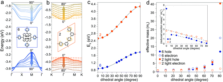 |
| | Fig. 3 (a) Valence and conduction bands plotted for different dihedral angles in structures 6 (a) and 2 (b). Dotted lines in (b) are valence and conduction bands, solid lines next lower/higher bands. (c) Dependence of the band gap on dihedral angle for 2 and 6. (d) Dependence of the effective masses on dihedral angle. Inset: Inverse of the reduced exciton mass as a function of dihedral angle. | |
2.4 Indirect gaps and metallic polymers
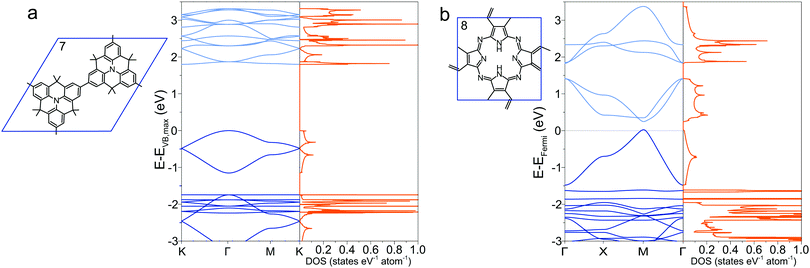
Most 2DPs calculated in this study are direct band-gap semiconductors with the Fermi level resting between valence and conduction band with few notable exceptions. Structures 5 described above exhibits a change from direct to indirect gap in the transition from single layer to 3D crystal. In addition, the heterotriangulene polymer 772,73 exhibits an indirect band gap of 1.80 eV between the Γ and the K point and a direct gap of 1.87 eV at the Γ point (Fig. 4a). The comparatively low band gap stems from the rather large conjugated organic repeat unit in the unit cell and the direct conjugation pathway that singles out this polymer from all other polymers with hexagonal unit cell. Notable is the Dirac cone feature at the K point about 0.5 eV below the valence band maximum. Dirac cones are also present in the band structures of the 2DPs 2, 3, and 4, which all share a hexagonal unit cell as common structural property. Through adequate doping it might be possible to convert these polymers into Dirac materials which can be used to study the physics of the Dirac cone. Phthalocyanine-based 2DP 8 (Fig. 4b), synthesized as a single sheets74 or found as building blocks in COFs39,41 has metallic character with the Fermi level crossing through one of the occupied bands. This stands in contrast to a previous study which reports a semiconductor with a direct band gap of 0.29 eV,75 in which a different unit cell was chosen to account for alternating positions of the hydrogen atoms in the macrocycle, effectively reducing the symmetry of the unit cell and hence possibly opening a band gap. The band gap in a B3LYP calculation is even larger with 0.59 eV.29 More refined computational methods are required to clear up the exact band structure of 8 and whether it really is a metallic organic polymer. Like 7, 2DP 8 is directly conjugated and additionally has several conjugated covalent bonds connecting adjacent molecular repeat units instead of only one as in all other structures, which is the reason for the non-existing (or very small) band gap. The density of states for both polymers shows appreciable occupation of conduction and valence bands exhibiting Van Hove singularities, promising interesting optical properties.
 |
| | Fig. 4 Band structure and density of states of (a) 7 and (b) 8. In (b), the Fermi level is set to zero. | |
2.5 Constitutional isomerization
To circumnavigate the cross-conjugation limitation found in phenyl-based 2DPs, other building blocks are investigated to synthesize directly conjugated polymers. One such molecule is the tetrathienoanthracene 9,47 which exhibits a band gap of 1.37 eV at the Γ point and large valence and conduction band dispersion (Fig. 5a). Its constitutional isomer 10, in which the position of the sulfur in the thiophene ring is altered, has a smaller band gap of 0.94 eV with similar band dispersion (Fig. 5b). A minor chemical modification by changing the position of sulfur in the molecule alters the electronic structure and the conjugation pathway dramatically in a way that the band diagrams of 9 and 10 appear dissimilar. Switching the position of the sulfur atom also reduces considerable the density of states at the conduction band maximum and valence band minimum in 10 compared to 9. The density of states has several Van Hove singularites, which depend strongly on the position of the sulfur atoms.
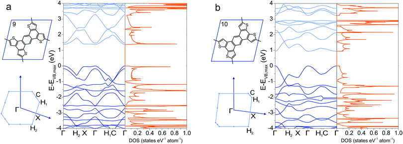 |
| | Fig. 5 Band structure and density of states of (a) 9 and (b) 10, together with their Brillouin zone. | |
A collection of the band gaps and unit cell parameters is given in Table 1. The PBE gaps are underestimated compared to more sophisticated theoretical approaches (hybrid exchange functionals and GW0). Already the limited set of structures presented in this work spans band gaps ranging from 0 to 3.59 eV. The effective masses given in Table 2 likewise span a wide range and are comparable to those calculated for 2D transition-metal dichalcogenides and oxides.76 As pictured in Fig. 3d, charge carrier mobility depends on the dihedral angle and is reduced by a factor of 10 in the energetically favorable geometry of 2DP 6 with 60° angle of the phenyl groups with respect to the macrocycle compared to the fully planar geometry of 2DP 6. The reduced exciton mass as a function of the band gap is plotted in Fig. 6a for all coplanar 2DPs. Light hole/electron masses are used to calculate the reduced exciton mass where applicable. The exciton masses correlate with band dispersion: the smaller the band gap, the larger the band dispersion and conversely the smaller the exciton mass. This can be intuitively understood by evoking an established simple picture that captures the physics of conjugated π-electron systems (Fig. 6b). By covalent linking molecular repeat units, the previously two separate highest occupied orbitals (HOMO) split into two occupied states, whereby one is energetically destabilized (shifted upward) with respect to the previous HOMO, the other is stabilized (shifted downward). The same occurs for the lowest occupied orbital (LUMO). The splitting depends on hybridization of the monomer levels in the newly formed dimer. This can be repeated by linking two dimers into a 2 × 2 dimer (linking the repeat units not linearly but in a plane) and subsequently into n × n oligomers, whereby the HOMO is successively shifted upward and the LUMO downward, reducing the band gap. In the complete polymer, separate molecular orbital levels lie so close that occupied valence bands and unoccupied conduction bands are formed. A detailed discussion of HOMO/LUMO position and gap reduction as a function of oligomer size in 2DPs is provided elsewhere.29 In this picture the trend depicted in Fig. 6a can then be rationalized as follows: conjugated polymers have two sources for a small band gap, one is the original HOMO/LUMO gap in the molecular repeat unit (monomer), i.e., the smaller this gap, the smaller the final band gap. The second source is the strength of hybridization between adjacent monomers in oligomers/polymers. Stronger hybridization leads to stronger orbital splitting, which is manifested in lower band gaps and larger dispersion of the bands. Care must be taken to not over-interpret this model since only excitons as a measure of band dispersion resulting from light holes and electrons are plotted in Fig. 6a, and only those of planar structures. Non-dispersive valence and conduction bands are frequently encountered, for example in 2DPs 2 and 3, which result from low hybridization of HOMO and LUMO between repeat units. Only the next orbitals, HOMO−1 and LUMO+1, evolve into dispersive bands. It is instructive to estimate the exciton binding energy in the simple Rydberg model, in which the electron–hole pair is described in analogy to an hydrogen atom. Assuming a dielectric constant of 3, the exciton binding energy measures few 100 meV to 1 eV. This is one to two orders of magnitude larger than the exciton binding energy of 3D inorganic semiconductors and comparable to 2D transition-metal dichalcogenides and oxides.76
Table 1 Band gaps Eg and unit cell vectors
| 2DP |
E
g (eV) |
Additional theoretical values (eV) |
a (nm) |
b (nm) |
Angle (°) |
|
Planar geometry.
Dihedral angle 30°.
Optimized dihedral angle ≈60°.
Dihedral angle 60°.
|
|
1
|
2.42 |
2.34 (LDA),51,52 2.40 (PW91),53 2.48 (PW91),54 3.2 (HSE06),51 3.91 (B3LYP)29 |
0.75 |
0.75 |
120 |
|
2
|
2.54 |
|
1.50 |
1.50 |
120 |
|
2
|
2.93 |
|
1.50 |
1.50 |
120 |
|
3
|
2.40 |
3.68 (B3LYP)29 |
2.26 |
2.26 |
120 |
|
3
|
3.59 |
5.01 (B3LYP)29 |
2.23 |
2.23 |
120 |
|
4
|
2.67 (1D, indirect), 2.21 (3D) |
2.65 (PBE),24 5.44 (GW0),24 2.42 (PBE)60 |
1.45 |
1.45 |
120 |
|
5
|
3.59 (1D), 2.69 (3D) |
3.6 (DFTB),23 3.55 (PBE),24 7.94 (GW0),24 3.50 (PBE)77 |
1.50 |
1.50 |
120 |
|
6
|
0.89 |
|
1.78 |
1.78 |
90 |
|
6
|
1.52 |
1.34 (tight-binding),70 2.62 (B3LYP, 71° angle)29 |
1.78 |
1.78 |
90 |
|
7
|
1.80 (indirect) |
3.08 (B3LYP)29 |
1.74 |
1.74 |
120 |
|
8
|
0 |
0.29 (PBE),75 0.59 (B3LYP)29 |
1.07 |
1.07 |
90 |
|
9
|
1.37 |
2.47 (B3LYP)29 |
1.20 |
1.20 |
71 |
|
10
|
0.94 |
1.79 (B3LYP)29 |
1.16 |
1.16 |
97 |
Table 2 Effective charge carrier masses (at k-point) and reduced exciton mass
| 2DP |
Hole mass (me) |
Electron mass (me) |
Exciton mass (me) |
|
Planar geometry.
Dihedral angle 30°.
Optimized dihedral angle ≈60°.
Dihedral angle 60°.
Light hole/electron.
|
|
1
|
1.28 (K) |
0.67 (K) |
0.44 |
|
2
|
1.36, 0.83e (Γ) |
1.39, 0.66e (Γ) |
0.69, 0.37e |
|
2
|
2.00, 1.12e (Γ) |
5.93, 0.84e (Γ) |
1.50, 0.48e |
|
3
|
5.45, 0.78e (Γ) |
42.83, 0.90e (Γ) |
4.83, 0.42e |
|
3
|
4.48, 2.60e (Γ) |
22.35, 1.05e (Γ) |
3.73, 0.75e |
|
4
|
3.04 (K) |
2.95, 0.56e (Γ) |
1.50, 0.47e |
|
5
|
30 (Γ) |
15, 0.63e (Γ) |
10, 0.62e |
|
6
|
0.25 (M) |
0.31 (M) |
0.14 |
|
6
|
2.49 (M) |
3.46 (M) |
1.45 |
|
7
|
0.32 (Γ) |
1.68 (K) |
0.27 |
|
9
|
0.31 (Γ) |
0.47 (Γ) |
0.19 |
|
10
|
0.26 (Γ) |
0.38 (Γ) |
0.15 |
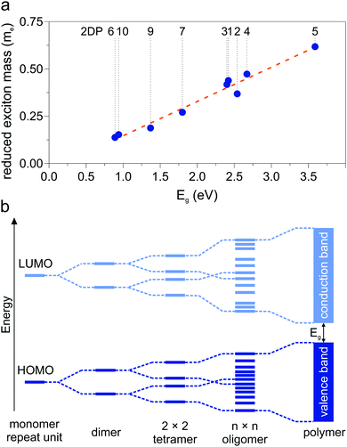 |
| | Fig. 6 (a) Reduced exciton mass as a function of band gap Eg for all coplanar polymers (light excitons). (b) Band formation from molecular repeat unit to π-conjugated polymer. | |
3 Conclusions
The presented conjugated 2D polymers exhibit intriguing band structures which depend on different factors such as the original molecular repeat unit in the unit cell, dihedral angles within a polymer sheet, number of layers, or constitutional isomerization. Band gaps and conduction/valence band dispersion depend on these parameters, which can be used for deliberate band-structure engineering. It is possible to synthesize polymers with non-dispersive bands, which have large density of states, suitable as strong light-absorbing materials. Other polymers have dispersive bands, more apt as conductive polymer sheets. There is an indirect correlation between band gap and dispersion of conduction/valence bands, which can be understood within a simple picture well-established for 1D conjugated polymers: the stronger the hybridization between occupied (unoccupied) orbitals, the smaller the band gap and the larger the dispersion of the valence (conduction) band. This translates into a direct relationship between the band gap and the reduced exciton mass of a polymer.
The diversity in the calculated band structures of 2DPs underlines their possible usefulness as materials with tailor-made electronic properties in numerous applications. Band-structure engineering through a suitable choice of monomeric building block and linking motifs can be used to design organic sheets with adjustable band gap and valence/conduction band dispersion, as well as density of states with characteristic Van Hove singularities. Dirac cones are features common to many of the 2DPs with hexagonal unit cell. The position of these cones with respect to valence band maximum and conduction band minimum depend on the structure of the organic backbone in the unit cell and it can be expected that 2DPs with Dirac cones close to the Fermi level can be experimentally realized. It is also clear that the band-structure engineering approach can likely be extended to electrically conductive metal–organic networks.78 However, if efficient charge transport within the polymer plane is the goal, for example as semiconductive channels in 2D field-effect transistors, new synthetic routes have to be investigated that circumnavigate the limitations of the abundant cross-conjugated polymers and which allow for the fabrication of directly conjugated polymers. Although experimental studies on the electronic structure of 2DPs are still scarce, future research should be able to probe relevant electronic characteristics detailed in this work. Of particular interest is the fabrication of lateral and vertical heterojunctions and heterostructures of 2DPs with differing band structure, which can be used as organic lasers, solar cells, or transistors. In addition, understanding the electronic structure of 2DPs will help to design COFs with desired catalytic properties.46,79
4 Methods
The Quantum Espresso 5.1 code was used for all calculations,80 employing a plane-wave basis set, the Perdew–Burke–Ernzerhof (PBE) functional,81 and normconserving Martins–Troullier pseudopotentials.82 All 2DPs were structurally relaxed in non-fixed unit cells (single-point calculations for varying dihedral angle in non-planar polymers were performed on optimized planar structures, in which only the dihedral angle was modified). An additional SCF step was performed on the optimized structure with a finer k-point grid. The vacuum along the z-direction perpendicular to the 2DP was ≥10 Å in all cases. For the multilayer calculation, a semiempirical van der Waals interaction was added.83 Unit cell vectors, number of k-points, and energy cut-offs are reported in excerpts of the input data for the SCF step before band structure calculation given in the ESI.† In the band-structure plots, the energy of the valence band maximum VB,max was set to 0. Effective electron and hole masses are calculated from the band plots by fitting parabola to the k-points in proximity to the valence band maximum and the conduction band minimum. The approximation of the exchange–correlation functional within the generalized gradient approximation through the PBE functional is known to underestimate band gaps and likely also effects the shape of the bands (dispersion). The values reported here are thus to be taken with care and do not establish exact numbers for comparison with experiment. However, a qualitative and relative comparison between band structures of different systems in a systematic study is achievable with this approximation and grants valuable insight into the electronic structure of 2DPs. The trends reported here are expected to be real and measurable.
Acknowledgements
Discussions with Vijay Vyas, Christian Schön, Claudius Morchutt, Klaus Kern, and Christian Ast are gratefully acknowledged.
References
- P. Miró, M. Audiffred and T. Heine, Chem. Soc. Rev., 2014, 43, 6537–6554 RSC.
- A. P. Côté, A. I. Benin, N. W. Ockwig, M. O'Keeffe, A. J. Matzger and O. M. Yaghi, Science, 2005, 310, 1166–1170 CrossRef PubMed.
- X. Feng, X. Ding and D. Jiang, Chem. Soc. Rev., 2012, 41, 6010–6022 RSC.
- P. J. Waller, F. Gándara and O. M. Yaghi, Acc. Chem. Res., 2015, 48, 3053–3063 CrossRef CAS PubMed.
- A. I. Cooper, Adv. Mater., 2009, 21, 1291–1295 CrossRef CAS.
- Y. Xu, S. Jin, H. Xu, A. Nagai and D. Jiang, Chem. Soc. Rev., 2013, 42, 8012–8031 RSC.
- S.-Y. Ding and W. Wang, Chem. Soc. Rev., 2013, 42, 548–568 RSC.
- J. W. Colson and W. R. Dichtel, Nat. Chem., 2013, 5, 453–465 CrossRef CAS PubMed.
- M. Dogru and T. Bein, Chem. Commun., 2014, 50, 5531–5546 RSC.
- P. Kissel, R. Erni, W. B. Schweizer, M. D. Rossell, B. T. King, T. Bauer, S. Götzinger, A. D. Schlüter and J. Sakamoto, Nat. Chem., 2012, 4, 287–291 CrossRef CAS PubMed.
- D. F. Perepichka and F. Rosei, Science, 2009, 323, 216–217 CrossRef CAS PubMed.
- G. Franc and A. Gourdon, Phys. Chem. Chem. Phys., 2011, 13, 14283–14292 RSC.
- M. Lackinger and W. M. Heckl, J. Phys. D: Appl. Phys., 2011, 44, 464011 CrossRef.
- M. El Garah, J. M. MacLeod and F. Rosei, Surf. Sci., 2013, 613, 6–14 CrossRef CAS.
- F. Klappenberger, Y.-Q. Zhang, J. Björk, S. Klyatskaya, M. Ruben and J. V. Barth, Acc. Chem. Res., 2015, 48, 2140–2150 CrossRef CAS PubMed.
- J. F. Dienstmaier, A. M. Gigler, A. J. Goetz, P. Knochel, T. Bein, A. Lyapin, S. Reichlmaier, W. M. Heckl and M. Lackinger, ACS Nano, 2011, 5, 9737–9745 CrossRef CAS PubMed.
- R. Tanoue, R. Higuchi, N. Enoki, Y. Miyasato, S. Uemura, N. Kimizuka, A. Z. Stieg, J. K. Gimzewski and M. Kunitake, ACS Nano, 2011, 5, 3923–3929 CrossRef CAS PubMed.
- C.-Z. Guan, D. Wang and L.-J. Wan, Chem. Commun., 2012, 48, 2943–2945 RSC.
- L. Xu, X. Zhou, W. Q. Tian, T. Gao, Y. F. Zhang, S. Lei and Z. F. Liu, Angew. Chem., Int. Ed., 2014, 53, 9564–9568 CrossRef CAS PubMed.
- I. Berlanga, M. L. Ruiz-González, J. M. González-Calbet, J. L. Fierro, R. Mas-Ballesté and F. Zamora, Small, 2011, 7, 1207–1211 CrossRef CAS PubMed.
- S. Chandra, S. Kandambeth, B. P. Biswal, B. Lukose, S. M. Kunjir, M. Chaudhary, R. Babarao, T. Heine and R. Banerjee, J. Am. Chem. Soc., 2013, 135, 17853–17861 CrossRef CAS PubMed.
- D. N. Bunck and W. R. Dichtel, J. Am. Chem. Soc., 2013, 135, 14952–14955 CrossRef CAS PubMed.
- B. Lukose, A. Kuc, J. Frenzel and T. Heine, Beilstein J. Nanotechnol., 2010, 1, 60–70 CrossRef CAS PubMed.
- P. Zhu and V. Meunier, J. Chem. Phys., 2012, 137, 244703 CrossRef CAS PubMed.
- Y. Zhou, Z. Wang, P. Yang, X. Zu and F. Gao, J. Mater. Chem., 2012, 22, 16964–16970 RSC.
- G. V. Baryshnikov, B. F. Minaev, N. N. Karaush and V. A. Minaeva, RSC Adv., 2014, 4, 25843–25851 RSC.
- J.-J. Adjizian, P. Briddon, B. Humbert, J.-L. Duvail, P. Wagner, C. Adda and C. Ewels, Nat. Commun., 2014, 5, 5842 CrossRef CAS PubMed.
- L. Liang, P. Zhu and V. Meunier, J. Chem. Phys., 2015, 142, 184708 CrossRef PubMed.
- R. Gutzler and D. F. Perepichka, J. Am. Chem. Soc., 2013, 135, 16585–16594 CrossRef CAS PubMed.
- A. N. Enyashin and A. L. Ivanovskii, Phys. Status Solidi B, 2011, 248, 1879–1883 CrossRef CAS.
- A. L. Ivanovskii, Prog. Solid State Chem., 2013, 41, 1–19 CrossRef CAS.
- M. A. Hudspeth, B. W. Whitman, V. Barone and J. E. Peralta, ACS Nano, 2010, 4, 4565–4570 CrossRef CAS PubMed.
- F. Schlütter, T. Nishiuchi, V. Enkelmann and K. Müllen, Angew. Chem., Int. Ed., 2014, 53, 1538–1542 CrossRef PubMed.
- N. N. Karaush, G. V. Baryshnikov and B. F. Minaev, Chem. Phys. Lett., 2014, 612, 229–233 CrossRef CAS.
- N. N. Karaush, S. V. Bondarchuk, G. V. Baryshnikov, V. A. Minaeva, W.-H. Sun and B. F. Minaev, RSC Adv., 2016, 6, 49505–49516 RSC.
- Z. Wang, X.-F. Zhou, X. Zhang, Q. Zhu, H. Dong, M. Zhao and A. R. Oganov, Nano Lett., 2015, 15, 6182–6186 CrossRef CAS PubMed.
- Y. Liu, G. Wang, Q. Huang, L. Guo and X. Chen, Phys. Rev. Lett., 2012, 108, 225505 CrossRef PubMed.
- S. Wan, J. Guo, J. Kim, H. Ihee and D. Jiang, Angew. Chem., Int. Ed., 2009, 48, 5439–5442 CrossRef CAS PubMed.
- X. Ding, J. Guo, X. Feng, Y. Honsho, J. Guo, S. Seki, P. Maitarad, A. Saeki, S. Nagase and D. Jiang, Angew. Chem., Int. Ed., 2011, 50, 1289–1293 CrossRef CAS PubMed.
- S. Wan, F. Gándara, A. Asano, H. Furukawa, A. Saeki, S. K. Dey, L. Liao, M. W. Ambrogio, Y. Y. Botros, X. Duan, S. Seki, J. F. Stoddart and O. M. Yaghi, Chem. Mater., 2011, 23, 4094–4097 CrossRef CAS.
- S. Jin, X. Ding, X. Feng, M. Supur, K. Furukawa, S. Takahashi, M. Addicoat, M. E. El-Khouly, T. Nakamura, S. Irle, S. Fukuzumi, A. Nagai and D. Jiang, Angew. Chem., Int. Ed., 2013, 52, 2017–2021 CrossRef CAS PubMed.
- X. Feng, L. Chen, Y. Honsho, O. Saengsawang, L. Liu, L. Wang, A. Saeki, S. Irle, S. Seki, Y. Dong and D. Jiang, Adv. Mater., 2012, 24, 3026–3031 CrossRef CAS PubMed.
- J. Guo, Y. Xu, S. Jin, L. Chen, T. Kaji, Y. Honsho, M. A. Addicoat, J. Kim, A. Saeki, H. Ihee, S. Seki, S. Irle, M. Hiramoto, J. Gao and D. Jiang, Nat. Commun., 2013, 4, 2736 Search PubMed.
- M. Dogru, M. Handloser, F. Auras, T. Kunz, D. Medina, A. Hartschuh, P. Knochel and T. Bein, Angew. Chem., Int. Ed., 2013, 52, 2920–2924 CrossRef CAS PubMed.
- V. S. Vyas, F. Haase, L. Stegbauer, G. Savasci, F. Podjaski, C. Ochsenfeld and B. V. Lotsch, Nat. Commun., 2015, 6, 8508 CrossRef CAS PubMed.
- R. S. Sprick, J.-X. Jiang, B. Bonillo, S. Ren, T. Ratvijitvech, P. Guiglion, M. A. Zwijnenburg, D. J. Adams and A. I. Cooper, J. Am. Chem. Soc., 2015, 137, 3265–3270 CrossRef CAS PubMed.
- L. Cardenas, R. Gutzler, J. Lipton-Duffin, C. Fu, J. L. Brusso, L. E. Dinca, M. Vondráček, Y. Fagot-Revurat, D. Malterre, F. Rosei and D. F. Perepichka, Chem. Sci., 2013, 4, 3263–3268 RSC.
- A. Wiengarten, K. Seufert, W. Auwärter, D. Ecija, K. Diller, F. Allegretti, F. Bischoff, S. Fischer, D. A. Duncan, A. C. Papageorgiou, F. Klappenberger, R. G. Acres, T. H. Ngo and J. V. Barth, J. Am. Chem. Soc., 2014, 136, 9346–9354 CrossRef CAS PubMed.
- M. Bieri, M. Treier, J. Cai, K. Aït-Mansour, P. Ruffieux, O. Gröning, P. Gröning, M. Kastler, R. Rieger, X. Feng, K. Müllen and R. Fasel, Chem. Commun., 2009, 6919–6921 RSC.
- M. Bieri, M.-T. Nguyen, O. Gröning, J. Cai, M. Treier, K. Aït-Mansour, P. Ruffieux, C. A. Pignedoli, D. Passerone, M. Kastler, K. Müllen and R. Fasel, J. Am. Chem. Soc., 2010, 132, 16669–16676 CrossRef CAS PubMed.
- A. Du, Z. Zhu and S. C. Smith, J. Am. Chem. Soc., 2010, 132, 2876–2877 CrossRef CAS PubMed.
- Y. Ding, Y. Wang, S. Shi and W. Tang, J. Phys. Chem. C, 2011, 115, 5334–5343 CAS.
- R. Lu, Z. Meng, E. Kan, F. Li, D. Rao, Z. Lu, J. Qian, C. Xiao, H. Wu and K. Deng, Phys. Chem. Chem. Phys., 2013, 15, 666–670 RSC.
- Y. Li, Z. Zhou, P. Shen and Z. Chen, Chem. Commun., 2010, 46, 3672–3674 RSC.
- M. H. van der Veen, M. T. Rispens, H. T. Jonkman and J. C. Hummelen, Adv. Funct. Mater., 2004, 14, 215–223 CrossRef CAS.
- J. Liu, P. Ruffieux, X. Feng, K. Müllen and R. Fasel, Chem. Commun., 2014, 50, 11200–11203 RSC.
- R. Gutzler, H. Walch, G. Eder, S. Kloft, W. M. Heckl and M. Lackinger, Chem. Commun., 2009, 4456–4458 RSC.
- M. O. Blunt, J. C. Russell, N. R. Champness and P. H. Beton, Chem. Commun., 2010, 46, 7157–7159 RSC.
- N. A. A. Zwaneveld, R. Pawlak, M. Abel, D. Catalin, D. Gigmes, D. Bertin and L. Porte, J. Am. Chem. Soc., 2008, 130, 6678–6679 CrossRef CAS PubMed.
- X. Jiang, P. Wang and J. Zhao, J. Mater. Chem. A, 2015, 3, 7750–7758 CAS.
- J. L. Brédas, J. P. Calbert, D. A. da Silva Filho and J. Cornil, Proc. Natl. Acad. Sci. U. S. A., 2002, 99, 5804–5809 CrossRef PubMed.
- J. Torras, J. Casanovas and C. Alemán, J. Phys. Chem. A, 2012, 116, 7571–7583 CrossRef CAS PubMed.
- J. K. Ellis, M. J. Lucero and G. E. Scuseria, Appl. Phys. Lett., 2011, 99, 261908 CrossRef.
- X. Feng, L. Liu, Y. Honsho, A. Saeki, S. Seki, S. Irle, Y. Dong, A. Nagai and D. Jiang, Angew. Chem., Int. Ed., 2012, 51, 2618–2622 CrossRef CAS PubMed.
- L. Grill, M. Dyer, L. Lafferentz, M. Persson, M. V. Peters and S. Hecht, Nat. Nanotechnol., 2007, 2, 687–691 CrossRef CAS PubMed.
- S. Krasnikov, C. Doyle, N. Sergeeva, A. Preobrajenski, N. Vinogradov, Y. Sergeeva, A. Zakharov, M. Senge and A. Cafolla, Nano Res., 2011, 4, 376–384 CrossRef CAS.
- X. Liu, Y. Xu, Z. Guo, A. Nagai and D. Jiang, Chem. Commun., 2013, 49, 3233–3235 RSC.
- S. J. Silvers and A. Tulinsky, J. Am. Chem. Soc., 1967, 89, 3331–3337 CrossRef CAS PubMed.
- F. Klappenberger, A. Weber-Bargioni, W. Auwärter, M. Marschall, A. Schiffrin and J. V. Barth, J. Chem. Phys., 2008, 129, 214702 CrossRef CAS PubMed.
- K. Tanaka, N. Kosai, H. Maruyama and H. Kobayashi, Synth. Met., 1998, 92, 253–258 CrossRef CAS.
-
G. Grosso and G. P. Parravicini, Solid State Physics, Academic Press, San Diego, California, USA, 2nd edn, 2003 Search PubMed.
- M. Bieri, S. Blankenburg, M. Kivala, C. A. Pignedoli, P. Ruffieux, K. Müllen and R. Fasel, Chem. Commun., 2011, 47, 10239–10241 RSC.
- F. Schlütter, F. Rossel, M. Kivala, V. Enkelmann, J.-P. Gisselbrecht, P. Ruffieux, R. Fasel and K. Müllen, J. Am. Chem. Soc., 2013, 135, 4550–4557 CrossRef PubMed.
- M. Abel, S. Clair, O. Ourdjini, M. Mossoyan and L. Porte, J. Am. Chem. Soc., 2011, 133, 1203–1205 CrossRef CAS PubMed.
- J. Zhou and Q. Sun, J. Am. Chem. Soc., 2011, 133, 15113–15119 CrossRef CAS PubMed.
- F. A. Rasmussen and K. S. Thygesen, J. Phys. Chem. C, 2015, 119, 13169–13183 CAS.
- R.-N. Wang, X.-R. Zhang, S.-F. Wang, G.-S. Fu and J.-L. Wang, Phys. Chem. Chem. Phys., 2016, 18, 1258–1264 RSC.
- L. Sun, M. G. Campbell and M. Dincă, Angew. Chem., Int. Ed., 2016, 55, 3566–3579 CrossRef CAS PubMed.
- V. S. Vyas, V. W. Lau and B. V. Lotsch, Chem. Mater., 2016, 28, 5191–5204 CrossRef CAS.
- P. Giannozzi, S. Baroni, N. Bonini, M. Calandra, R. Car, C. Cavazzoni, D. Ceresoli, G. L. Chiarotti, M. Cococcioni, I. Dabo, A. Dal Corso, S. de Gironcoli, S. Fabris, G. Fratesi, R. Gebauer, U. Gerstmann, C. Gougoussis, A. Kokalj, M. Lazzeri, L. Martin-Samos, N. Marzari, F. Mauri, R. Mazzarello, S. Paolini, A. Pasquarello, L. Paulatto, C. Sbraccia, S. Scandolo, G. Sclauzero, A. P. Seitsonen, A. Smogunov, P. Umari and R. M. Wentzcovitch, J. Phys.: Condens. Matter, 2009, 21, 395502 CrossRef PubMed.
- J. P. Perdew, K. Burke and M. Ernzerhof, Phys. Rev. Lett., 1996, 77, 3865–3868 CrossRef CAS PubMed.
- N. Troullier and J. L. Martins, Phys. Rev. B: Condens. Matter Mater. Phys., 1991, 43, 1993–2006 CrossRef CAS.
- S. Grimme, J. Comput. Chem., 2006, 27, 1787–1799 CrossRef CAS PubMed.
Footnote |
| † Electronic supplementary information (ESI) available: SCF input file excerpts: cut-off frequency, k-points, optimized unit cell and atomic coordinates. See DOI: 10.1039/c6cp06101j |
|
| This journal is © the Owner Societies 2016 |

 Open Access Article
 This Open Access Article is licensed under a

 are plotted as a function of dihedral angle in Fig. 3d. Only the light electron and hole masses are plotted for 2 as they stem from more dispersive bands than the valence and conduction bands. The effective mass depends superlinearly on the rotational angle and is similarly pronounced in 6 and in 2. The reduced effective exciton mass
 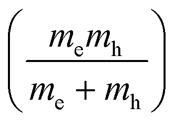 71 depends inversely on the dihedral angle with similar slopes for 2 and 6 (inset Fig. 3d, the outlier of 6 at 0° is excluded from the linear fit). Larger deviations from planarity thus lead to more localized excitons on the polymer. As discussed above, the dihedral angle in the polymer sheet depends heavily on its environment, whether it is a free-standing sheet, resting as a layer in a COF, or sitting on a surface. The (optical) gap and charge transport within the sheet will hence likewise depend on the environment.


