 Open Access Article
Creative Commons Attribution 3.0 Unported Licence
Large-area synthesis of monolayer MoSe2 films on SiO2/Si substrates by atmospheric pressure chemical vapor deposition
Yu Zhaoab,
Hyunjea Leec,
Woong Choi*d,
Weidong Feib and
Cheol Jin Lee *ac
*ac
aDepartment of Micro/Nano Systems, Korea University, Seoul 02841, Korea. E-mail: cjlee@korea.ac.kr
bSchool of Materials Science and Engineering, Harbin Institute of Technology, Harbin 150001, PR China
cSchool of Electrical Engineering, Korea University, Seoul 02841, Korea
dSchool of Advanced Materials Engineering, Kookmin University, Seoul 02707, Korea. E-mail: woongchoi@kookmin.ac.kr
First published on 26th May 2017
Abstract
We report the synthesis of large-scale continuous MoSe2 films on SiO2/Si substrates by atmospheric pressure chemical vapor deposition (CVD). As-grown thin films were composed of a continuous monolayer of MoSe2 and extended up to a millimeter scale. The CVD-grown monolayer MoSe2 films were uniform in thickness and highly crystalline with hexagonal crystal structures. Raman and photoluminescence spectra showed that CVD-grown monolayer MoSe2 films have similar vibrational and optical properties to those of mechanically exfoliated monolayer MoSe2. These results demonstrate that the CVD-grown monolayer MoSe2 films have reasonably high quality comparable to that of mechanically exfoliated monolayer MoSe2 flakes.
Introduction
In recent years, transition metal dichalcogenides (TMDs) with an atomically thin two-dimensional layer structure have attracted enormous attention because of their excellent electronic and optical properties.1–8 The band gap of TMDs semiconductors (1–2 eV) makes them promising candidates for the channel materials of field-effect transistors (FETs).9–11 Moreover, TMDs materials such as MoS2 or MoSe2 show indirect-to-direct bandgap transition when their thickness decreases down to monolayer.12,13 This suggests that monolayer TMDs semiconductors are very promising for potential applications in optoelectronic devices such as photo detectors.14,15So far, various methods have been tried to obtain large-area TMDs films as the synthesis of large-area TMDs is one of the critical challenges for their real applications. Most emphasis has been put on MoS2. Mechanical exfoliation provides high-quality crystalline flakes. But, their size is limited, the number of layer is uncontrollable, and the product yield is very low.4,16,17 Chemical exfoliation and electrochemical exfoliation provide a simple and easy way but obtained flakes are small in the size and uncontrollable in thickness.18,19 Sulfurization of transition metals or transition metal oxides provides large-area films, but obtained films show uncontrollable thickness uniformity.20 In comparison, chemical vapor deposition (CVD) with solid-phase precursors (such as S and MoO3 powder) can provide an effective method to synthesize monolayer MoS2 with reasonable quality on different substrates including SiO2/Si wafers, metal foils, or sapphire wafers.21–24 Moreover, CVD with metalorganic (MO) precursors can provide wafer-scale continuous MoS2 films.25
The use of MoSe2 could be more suitable than MoS2 for the application of tunnel FETs, optoelectronic devices and spintronic devices with its narrower bandgap,13 higher optical absorbance26 and larger spin-splitting energy27 than MoS2. However, compared to CVD-grown monolayer MoS2, there have been much less reports on CVD-grown monolayer MoSe2.28–37 Thin films of MoSe2 has not yet been obtained by CVD with MO precursors. Furthermore, it is much more difficult to synthesize monolayer MoSe2 films by CVD with solid-phase precursors than monolayer MoS2 films because of the low chemical reactivity of Se. CVD with solid-phase precursors commonly results in triangular-shaped discontinuous domains of either single-layer MoSe2 or mixtures of single- and few-layer MoSe2.28–30,32–35,37 While continuous thin films of monolayer MoSe2 can be obtained on substrates up to about 1 cm2 in size by meticulously tuning and optimizing experimental parameters of low pressure CVD processes,36 continuous MoSe2 films with such size have not yet been reported by atmospheric pressure CVD. As atmospheric pressure CVD can allow higher deposition rate and lower substrate temperature than low pressure CVD in general, it is still of interest to synthesize large-area MoSe2 films with a uniform thickness by atmospheric pressure CVD. Here, we demonstrate the synthesis of large-area monolayer MoSe2 films extended up to a millimeter scale on SiO2/Si substrates by atmospheric pressure CVD. The obtained monolayer MoSe2 shows very uniform film thickness, good continuity, highly crystalline hexagonal crystal structures. Furthermore, we compare for the first time the vibrational and optical properties of monolayer MoSe2 thin films to those of mechanically exfoliated monolayer MoSe2 single crystals.
Experimental
The schematic illustration of the synthesis of MoSe2 films is shown in Fig. 1. The atmospheric pressure CVD reaction was carried out using a two-zone horizontal tube furnace with a one inch diameter quartz tube. Se powder was loaded in an alumina boat at the center of zone 1, and MoO3 powder was loaded in an alumina boat at the center of zone 2. A 300 nm-SiO2/Si substrate was located at the center of zone 2 with its face down on another alumina boat. During the synthesis of MoSe2 film, zone 1 was heated to 300 °C with flowing Ar/H2 carrier gases under atmospheric pressure while zone 2 was heated to 750 °C. The Ar and H2 flow rates were 1500 sccm and 150 sccm, respectively. Se powder was evaporated at the center of zone 1 and transported to zone 2 downstream by Ar carrier gas, and MoO3 powder was reduced by H2 gas at the same time. The selenization of vapor-phase Mo produced nucleation of MoSe2 species on the SiO2/Si substrate. Finally, the nucleated MoSe2 species grew into large-area MoSe2 films. It is well understood that hydrogen plays a critical role in the growth of MoSe2 films as an additional reducing agent with Se and MoO3 powder precursors.30,38 MoSe2 films were not observed on the substrates without H2 gas.Results and discussion
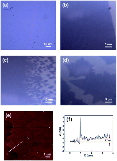
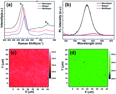
Fig. 2(a)–(d) show the optical images of as-grown MoSe2. The area covered with monolayer MoSe2 looks dark while uncovered area looks bright. The monolayer MoSe2 films with several hundred micrometers were found on SiO2/Si substrates as shown in Fig. 2(a) and (b) (we intentionally scratched the surface to leave the pink colored line). Fig. 2(c) shows some triangular domains of MoSe2 with several micrometers on SiO2/Si substrates. Those domains merge together and become a continuous and large-area film up to several hundred micrometers. Partly some triangular domains are folded, resulting in bilayers or triple layers as shown in Fig. 2(d). The homogeneous color of MoSe2 films in optical images suggests that the as-grown MoSe2 films have good continuity and uniformity. Atomic force microscopy (AFM) was used to measure the morphology and the thickness of the MoSe2 films. Fig. 2(e) and (f) show the AFM image and the height of as-grown MoSe2 film on the SiO2/Si substrate, respectively. The measured height is about 0.7 nm, which is consistent with the thickness of mechanically exfoliated monolayer MoSe2 flakes.Raman spectrum is an effective method to characterize layer numbers of TMDs materials. Fig. 3(a) shows the Raman spectra of as-grown mono-, bi-, and multilayer MoSe2 films with a 514 nm excitation laser. There are two main peaks in the Raman spectra, one is a sharp peak at low wavenumber corresponding to A1g mode (out of plane vibration), and another is a broad peak at high wavenumber corresponding to E2g mode (in plane vibration). In general, the location of Raman modes can be used to determine the thickness of TMDs materials. In this work, the A1g and E2g modes of monolayer MoSe2 films are located at 239.2 and 290.3 cm−1, respectively, which is well agreed with the previous results of 2H-phase exfoliated monolayer MoSe2 flakes and CVD-grown monolayer MoSe2 films.12,33 As the thickness of MoSe2 film increases from monolayer to multilayer, the A1g mode is blue-shifted to 240.2 cm−1, and the E2g mode is red-shifted to 285.9 cm−1. Similar results were also previously reported by other groups.15,30,32,33
In order to confirm the bandgap of CVD-grown MoSe2 films, photoluminescence (PL) spectra were measured. Fig. 3(b) shows the PL spectra of mono-, bi-, and multilayer MoSe2 films. A monolayer MoSe2 film shows a high intensity peak at 790 nm (1.57 eV), which can be ascribed to the direct bandgap at K point of Brillouin zone.13 The observed PL emission at 1.57 eV is in good agreement with the reported values in literature.32,33 The bandgap of MoSe2 changes from direct to indirect as the thickness increases from monolayer to multilayer. This significantly decreases PL peak intensity.13 The PL peak of bilayer MoSe2 films is red-shifted to 810 nm (1.53 eV), and the peak intensity is approximately 15 times weaker than that of monolayer MoSe2 films. This is also in good agreement with the results on MoSe2 bilayer in literature.33 Moreover, it is difficult to find noticeable peak intensity for multilayer MoSe2 films.
It is well known that Raman mapping can further confirm uniformity and continuity of the CVD-grown MoSe2 films. Fig. 3(c) and (d) show Raman mapping of monolayer MoSe2 films in the area of 40 × 40 μm2 where the distribution in A1g and E2g mode is presented, respectively. The uniform color of the two mapping images indicates that the CVD-grown MoSe2 films have considerably good uniformity and continuity. Raman and PL analysis suggests that our CVD-grown monolayer MoSe2 films are uniform in thickness.
In order to investigate elemental composition and binding energy of the as-grown monolayer MoSe2 films, X-ray photoelectron spectroscopy (XPS) was used. Carbon binding energy was set as a reference to remove any effects of charge accumulation on these samples, and the backgrounds were estimated as Shirley-type.28 Fig. 4(a) shows that MoSe2 films have the binding energy of 229.1 and 232.2 eV at Mo 3d5/2 and 3d3/2 peaks, respectively. In this work, the binding energies of Mo are significantly shifted from those of hexavalent Mo (∼232.5 and 235.9 eV), suggesting the reduction of Mo from Mo6+ (MoO3) to Mo4+.39 Fig. 4(b) shows the binding energies of 54.5 and 55.3 eV corresponding to divalent Se ions (Se 3d5/2 and 3d3/2, respectively). It is worth noting that XPS results are consistent with previous works in literature confirming the chemical valence states of the CVD-grown monolayer MoSe2 films.28,31
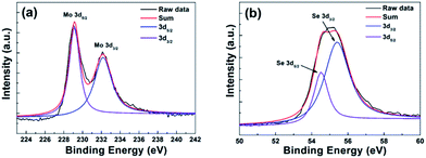 | ||
| Fig. 4 XPS characterization of monolayer MoSe2 film. (a) XPS spectra of Mo 3d binding energy and (b) XPS spectra of Se 3d binding energy. | ||
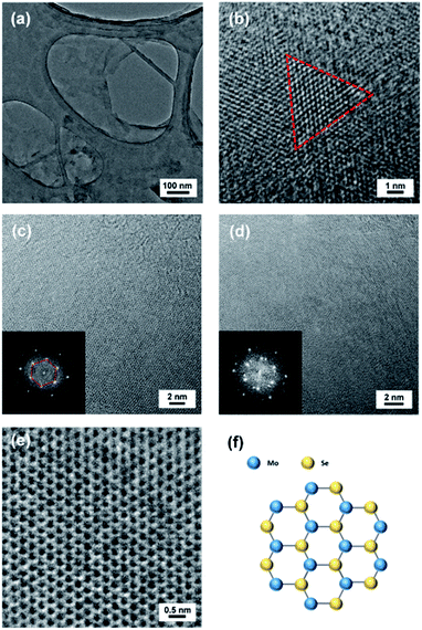
The crystal structure of CVD-grown monolayer MoSe2 films was characterized using transmission electron microscopy (TEM). The MoSe2 films were transferred to a carbon-coated Cu TEM grid. Fig. 5(a) shows that the transferred MoSe2 film has good continuity but some folds and small particles exist due to residual organics or unskillful transfer technique. Fig. 5(b) shows a triangular grain with several micrometers in size inside a continuous MoSe2 film, indicating the polycrystalline nature of CVD-grown monolayer MoSe2 films. Fig. 5(c) shows a TEM image of a monolayer MoSe2 film with a corresponding fast Fourier transformation (FFT) pattern in the inset. The FFT pattern exhibits clear six-fold symmetry of diffraction spots, demonstrating single layer MoSe2 film with a hexagonal structure. Fig. 5(d) shows a TEM image of a bilayer MoSe2 film with a corresponding FFT pattern in the inset. The FFT pattern indicates a twist between two layers with additional six diffraction spots. Fig. 5(e) clearly demonstrates the expected hexagonal crystal structure of monolayer MoSe2 in the high resolution TEM (HRTEM) image. The lattice constant is ∼0.3 nm, which is well agreed with the previous results of monolayer MoSe2.28,30,31,33 HRTEM images and FFT patterns confirm the high crystallinity of the CVD-grown monolayer MoSe2 films.
It needs to be mentioned that, while perfect 2H-phase MoS2 is known to be inert, defects such as vacancies and grain boundaries in real MoS2 can lead to poor long-term stability in air.40,41 As a theoretical calculation predicts comparable oxidation behavior between single layer MoS2 and MoSe2,40 we expect our CVD-grown MoSe2 thin films could be more resistant to oxidation with improved crystallinity in the future.
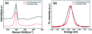
Finally, the quality of the CVD-grown monolayer MoSe2 film was compared to a mechanically exfoliated monolayer MoSe2 flake through Raman and PL spectra. Fig. 6(a) shows that Raman spectrum of CVD-grown monolayer MoSe2 film is consistent with that of an exfoliated monolayer MoSe2 flake, which indicates the high quality of the CVD-grown monolayer MoSe2 film. Even though the PL spectrum in Fig. 6(b) shows that the emission peak of CVD-grown monolayer MoSe2 film exhibits very similar intensity and energy to those of the mechanically exfoliated monolayer MoSe2 flake, the CVD-grown monolayer MoSe2 film shows a slightly wider full-width at half-maximum of PL peak than that of the mechanically exfoliated monolayer MoSe2 flake. It may imply that the CVD-grown monolayer MoSe2 film has a little higher defect density than that of the mechanically exfoliated monolayer MoSe2 flake. In fact, the interpretation of the crystal quality by optical analysis like Raman or PL is complicated to assess the crystal quality of two-dimensional materials.42 Nevertheless, these results suggest that the CVD-grown monolayer MoSe2 film has reasonably high quality comparable to that of the mechanically exfoliated monolayer MoSe2 flake.
Conclusions
We investigated the synthesis of large-area monolayer MoSe2 films on SiO2/Si substrates by atmospheric pressure CVD. The CVD-grown monolayer MoSe2 exhibited continuous and large- scale films with uniform thickness. The HRTEM images with corresponding FFT patterns revealed that CVD-grown monolayer MoSe2 films have hexagonal crystal structure with high crystallinity. Raman and PL spectra analysis showed that the CVD-grown monolayer MoSe2 films have comparable vibrational and optical properties with those of mechanically-exfoliated monolayer MoSe2 flakes. These results demonstrate that our large-area CVD-grown monolayer MoSe2 films have reasonably high quality comparable to that of the mechanically exfoliated monolayer MoSe2 flake. We suggest that our large-area and high quality CVD-grown monolayer MoSe2 films can expand understanding on the synthesis of TMDs materials, providing potentially important implications on their applications in various electronic and photonic devices in the future.Acknowledgements
This work was supported by Brain Korea 21 Plus Project (T1300304) and Carbon-based Technology for the Internet-of-Things Era Project (K1518861).References
- A. Splendiani, L. Sun, Y. Zhang, T. Li, J. Kim, C. Y. Chim, G. Galli and F. Wang, Nano Lett., 2010, 10, 1271–1275 CrossRef CAS PubMed.
- B. Radisavljevic, A. Radenovic, J. Brivio, V. Giacometti and A. Kis, Nat. Nanotechnol., 2011, 6, 147–150 CrossRef CAS PubMed.
- G. Eda, H. Yamaguchi, D. Voiry, T. Fujita, M. Chen and M. Chhowalla, Nano Lett., 2011, 11, 5111–5116 CrossRef CAS PubMed.
- Q. H. Wang, K. Kalantar-Zadeh, A. Kis, J. N. Coleman and M. S. Strano, Nat. Nanotechnol., 2012, 7, 699–712 CrossRef CAS PubMed.
- W. Choi, M. Y. Cho, A. Konar, J. H. Lee, G. B. Cha, S. C. Hong, S. Kim, J. Kim, D. Jena, J. Joo and S. Kim, Adv. Mater., 2012, 24, 5832–5836 CrossRef CAS PubMed.
- S. Kim, A. Konar, W.-S. Hwang, J. H. Lee, J. Lee, J. Yang, C. Jung, H. Kim, J.-B. Yoo, J.-Y. Choi, Y. W. Jin, S. Y. Lee, D. Jena, W. Choi and K. Kim, Nat. Commun., 2012, 3, 1011 CrossRef PubMed.
- H. Kwon, W. Choi, D. Lee, Y. Lee, J. Kwon, B. Yoo, C. P. Grigoropoulos and S. Kim, Nano Res., 2014, 7, 1137–1145 CrossRef CAS.
- H. T. Mohammad and J. S. Volker, Nanotechnology, 2015, 26, 344005 CrossRef PubMed.
- O. Lopez-Sanchez, D. Lembke, M. Kayci, A. Radenovic and A. Kis, Nat. Nanotechnol., 2013, 8, 497–501 CrossRef CAS PubMed.
- B. Chamlagain, Q. Li, N. J. Ghimire, H.-J. Chuang, M. M. Perera, H. Tu, Y. Xu, M. Pan, D. Xaio, J. Yan, D. Mandrus and Z. Zhou, ACS Nano, 2014, 8, 5079–5088 CrossRef CAS PubMed.
- D. Ovchinnikov, A. Allain, Y.-S. Huang, D. Dumcenco and A. Kis, ACS Nano, 2014, 8, 8174–8181 CrossRef CAS PubMed.
- K. F. Mak, C. Lee, J. Hone, J. Shan and T. F. Heinz, Phys. Rev. Lett., 2010, 105, 136805 CrossRef PubMed.
- S. Tongay, J. Zhou, C. Ataca, K. Lo, T. S. Matthews, J. Li, J. C. Grossman and J. Wu, Nano Lett., 2012, 12, 5576–5580 CrossRef CAS PubMed.
- H. R. Gutiérrez, N. Perea-López, A. L. Elías, A. Berkdemir, B. Wang, R. Lv, F. López-Urías, V. H. Crespi, H. Terrones and M. Terrones, Nano Lett., 2013, 13, 3447–3454 CrossRef PubMed.
- P. Tonndorf, R. Schmidt, P. Bottger, X. Zhang, J. Borner, A. Liebig, M. Albrecht, C. Kloc, O. Gordan, D. R. T. Zahn, S. M. de Vasconcellos and R. Bratschitsch, Opt. Express, 2013, 21, 4908–4916 CrossRef CAS PubMed.
- H. Li, J. Wu, Z. Yin and H. Zhang, Acc. Chem. Res., 2014, 47, 1067–1075 CrossRef CAS PubMed.
- M. Chhowalla, H. S. Shin, G. Eda, L.-J. Li, K. P. Loh and H. Zhang, Nat. Chem., 2013, 5, 263–275 CrossRef PubMed.
- J. N. Coleman, M. Lotya, A. O'Neill, S. D. Bergin, P. J. King, U. Khan, K. Young, A. Gaucher, S. De, R. J. Smith, I. V. Shvets, S. K. Arora, G. Stanton, H. Y. Kim, K. Lee, G. T. Kim, G. S Duesberg, T. Hallam, J. J. Boland, J. J. Wang, J. F. Donegan, J. C. Grunlan, G. Moriarty, A. Shmeliov, R. J. Nicholls, J. M. Perkins, E. M. Grieveson, K. Theuwissen, D. W. McComb, P. D. Nellist and V. Nicolosi, Science, 2011, 331, 568–571 CrossRef CAS PubMed.
- Z. Zeng, Z. Yin, X. Huang, H. Li, Q. He, G. Lu, F. Boey and H. Zhang, Angew. Chem., Int. Ed., 2011, 50, 11093–11097 CrossRef CAS PubMed.
- Y.-C. Lin, W. Zhang, J.-K. Huang, K.-K. Liu, Y.-H. Lee, C.-T. Liang, C.-W. Chu and L.-J. Li, Nanoscale, 2012, 4, 6637–6641 RSC.
- Y.-H. Lee, L. Yu, H. Wang, W. Fang, X. Ling, Y. Shi, C.-T. Lin, J.-K. Huang, M.-T. Chang, C.-S. Chang, M. Dresselhaus, T. Palacios, L.-J. Li and J. Kong, Nano Lett., 2013, 13, 1852–1857 CrossRef CAS PubMed.
- J. Shi, D. Ma, G.-F. Han, Y. Zhang, Q. Ji, T. Gao, J. Sun, X. Song, C. Li, Y. Zhang, X.-Y. Lang, Y. Zhang and Z. Liu, ACS Nano, 2014, 8, 10196–10204 CrossRef CAS PubMed.
- L. Ma, D. N. Nath, E. W. Lee, C. H. Lee, M. Yu, A. Arehart, S. Rajan and Y. Wu, Appl. Phys. Lett., 2014, 105, 072105 CrossRef.
- W. Shanshan, P. Merce, B. Harish and H. W. Jamie, Nanotechnology, 2016, 27, 085604 CrossRef PubMed.
- K. Kang, S. Xie, L. Huang, Y. Han, P. Y. Huang, K. F. Mak, C.-J. Kim, D. Muller and J. Par, Nature, 2015, 520, 656–660 CrossRef CAS PubMed.
- M. Bernardi, M. Palummo and J. C. Grossman, Nano Lett., 2013, 13, 3664 CrossRef CAS PubMed.
- Y. Zhang, T.-R. Chang, B. Zhou, Y.-T. Cui, H. Yan, Z. Liu, F. Schmitt, J. Lee, R. Moore, Y. Chen, H. Lin, H.-T. Jeng, S.-K. Mo, Z. Hussain, A. Bansil and Z.-X. Shen, Nat. Nanotechnol., 2014, 9, 111 CrossRef CAS PubMed.
- Y. H. Chang, W. Zhang, Y. Zhu, Y. Han, J. Pu, J. K. Chang, W. T. Hsu, J. K. Huang, C. L. Hsu, M. H. Chiu, T. Takenobu, H. Li, C. I. Wu, W. H. Chang, A. T. S. Wee and L. J. Li, ACS Nano, 2014, 8, 8582–8590 CrossRef CAS PubMed.
- A. Bachmatiuk, R. F. Abelin, H. T. Quang, B. Trzebicka, J. Eckert and M. H. Rummeli, Nanotechnology, 2014, 25, 365603 CrossRef CAS PubMed.
- J. Shaw, H. Zhou, Y. Chen, N. Weiss, Y. Liu, Y. Huang and X. Duan, Nano Res., 2014, 7, 511–517 CrossRef CAS.
- X. Wang, Y. Gong, G. Shi, W. L. Chow, K. Keyshar, G. Ye, R. Vajtai, J. Lou, Z. Liu, E. Ringe, B. K. Tay and P. M. Ajayan, ACS Nano, 2014, 8, 5125–5131 CrossRef CAS PubMed.
- X. Lu, M. I. B. Utama, J. H. Lin, X. Gong, J. Zhang, Y. Y. Zhao, S. T. Pantelides, J. X. Wang, Z. L. Dong, Z. Liu, W. Zhou and Q. H. Xiong, Nano Lett., 2014, 14, 2419–2425 CrossRef CAS PubMed.
- J. Xia, X. Huang, L.-Z. Liu, M. Wang, L. Wang, B. Huang, D.-D. Zhu, J.-J. Li, C.-Z. Gu and X.-M. Meng, Nanoscale, 2014, 6, 8949–8955 RSC.
- G. W. Shim, K. Yoo, S.-B. Seo, J. Shin, D. Y. Jung, I.-S. Kang, C. W. Ahn, B. J. Cho and S.-Y. Choi, ACS Nano, 2014, 8, 6655–6662 CrossRef CAS PubMed.
- C. Jung, S. M. Kim, H. Moon, G. Han, J. Kwon, Y. K. Hong, I. Omkaram, Y. Yoon, S. Kim and J. Park, Sci. Rep., 2015, 5, 15313 CrossRef CAS PubMed.
- Y. Gong, G. Ye, S. Lei, G. Shi, Y. He, J. Lin, X. Zhang, R. Vajtai, S. T. Pantelides, W. Zhou, B. Li and P. M. Ajayan, Adv. Funct. Mater., 2016, 26, 2009–2015 CrossRef CAS.
- H. Liu, Z. Chen, X. Chen, S. Chu, J. Huang and R. Peng, J. Mater. Chem. C, 2016, 4, 9399–9404 RSC.
- J.-K. Huang, J. Pu, C.-L. Hsu, M.-H. Chiu, Z.-Y. Juang, Y. H. Chang, W.-H. Chang, Y. Iwasa, T. Takenobu and L.-J. Li, ACS Nano, 2014, 8, 923–930 CrossRef CAS PubMed.
- M. Bougouma, A. Batan, B. Guel, T. Segato, J. B. Legma, F. Reniers, M.-P. Delplancke-Ogletree, C. Buess-Herman and T. Doneux, J. Cryst. Growth, 2013, 363, 122–127 CrossRef CAS.
- H. Liu, N. Han and J. Zhao, RSC Adv., 2015, 5, 17572–17581 RSC.
- J. Gao, B. Li, J. Tan, P. Chow, T.-M. Lu and N. Koratkar, ACS Nano, 2016, 10, 2628–2635 CrossRef CAS PubMed.
- S. Tongay, J. Suh, C. Ataca, W. Fan, A. Luce, J. S. Kang, J. Liu, C. Ko, R. Raghunathanan, J. Zhou, F. Ogletree, J. B. Li, J. C. Grossman and J. Wu, Sci. Rep., 2013, 3, 2657 CrossRef PubMed.
| This journal is © The Royal Society of Chemistry 2017 |


