Highly efficient organic p–i–n photovoltaic cells based on tetraphenyldibenzoperiflanthene and fullerene C70†
Zhongqiang
Wang
a,
Daisuke
Yokoyama
*a,
Xiao-Feng
Wang
a,
Ziruo
Hong
*a,
Yang
Yang
*b and
Junji
Kido
a
aResearch Center for Organic Electronics and Department of Organic Device Engineering, Yamagata University, 4-3-16 Jonan, Yonezawa, Yamagata 992-8510, Japan. E-mail: d_yokoyama@yz.yamagata-u.ac.jp; ziruo@yz.yamagata-u.ac.jp
bDepartment of Materials Science and Engineering, University of California-Los Angeles, Los Angeles, CA 90095, USA. E-mail: yangy@ucla.edu
First published on 23rd October 2012
Abstract
In this work, tetraphenyldibenzoperiflanthene (DBP) and fullerene C70 were used to construct organic photovoltaic cells. A power conversion efficiency of 5.19% was obtained by inserting a blend layer of DBP and C70 between the two neat layers, i.e. the so-called p–i–n structure, while the bilayer cell has an efficiency of 3.56%. The significant enhancement in photocurrent was mainly ascribed to absorption of the blend film. Interestingly optical characterization revealed that DBP molecules in the blend film showed a preferable orientation parallel to the substrate surface, suggesting that anisotropic properties can be realized in vacuum deposited donor–acceptor blend films for efficient light harvesting. Photoresponse of the p–i–n cells extended into the spectral range longer than band-edge absorption of the two materials, which is clearly associated with formation of charge transfer states between the DBP donor and C70 acceptor. On the other hand, the charge transfer states cause increase of saturation current of the diodes, and thus decrease of open circuit voltage. Our results indicate that the controversial effects of such charge transfer states should be considered in organic solar cells with respect to material selection and device design.
Broader contextSolar cells provide feasible solutions to the upcoming energy crisis due to limited availability of fossil fuels, delivering electricity without any CO2 emission. From viewpoints of material selection and manufacturing technology, organic material based photovoltaic cells have the potential to convert solar power into electricity at an affordable price with minimal environmental impacts. One of the major challenges of organic photovoltaic cells in practical applications is the inferior power conversion efficiency relative to that of Si based solar cells. To promote the efficiency, it is important to understand the interaction between electron donor and acceptor molecules in organic heterojunction systems. We chose a model system using tetraphenyldibenzoperiflanthene as a donor with a rigid and co-planar conjugated backbone in combination with fullerene C70 as an acceptor. Compared to normal planar heterojunction cells, significant enhancement in photocurrent was observed from p–i–n type organic photovoltaic cells, and hence a power conversion efficiency of >5% was demonstrated. Formation of ground state charge-transfer states and molecular orientation in the donor–acceptor blend layer were observed, and correlation of ground-state charge transfer with open circuit voltage was discussed, revealing an alternative way to control the effective bandgap in organic heterojunction solar cells. |
1. Introduction
Photoinduced charge transfer in organic donor–acceptor (D–A) systems enables exciton dissociation into free carriers with near unity efficiency.1,2 So far, organic photovoltaic (OPV) cells have been regarded as promising candidates for photon-to-electron conversion devices, i.e. solar cells and photodetectors.3 Typically external quantum efficiency (EQE), ηEQE, is determined by four factors, i.e.| ηEQE = ηAbs × ηED × ηCG × ηCC, |
The photon energy has to exceed the bandgap of the materials in order to facilitate the electronic transition from ground to excited states. Alternatively, it has been recognized that ground-state charge transfer states might form and have photoresponse in organic heterojunctions.4–6 Such electronic transitions are limited by the orbital overlap between donor and acceptor molecules.7 Therefore it is weak in comparison to the intrinsic absorption of individual molecules.
In a layer-by-layer structure referred to as planar heterojunction OPV cells,2 exciton generation is dominated by intrinsic absorption of both donor and acceptor layers, and thus has little to do with the interface, since planar heterojunction has minimized the donor–acceptor interface. In such a structure, the exciton dissociation was limited by the short exciton diffusion length, usually on the order of 10 nm in organic amorphous films,3 while to achieve sufficient light absorption it requires a thickness of at least 50 nm.8 The concept of bulk heterojunction was then introduced, in which donor and acceptor materials are mixed in the same layer. Exciton separation may occur everywhere throughout the bulk film due to the intimate contact between donor and acceptor molecules.9
Pioneered by Hiramoto et al.,10 a donor–acceptor blend film can be inserted between donor and acceptor layers, resulting in a p–i–n architecture.11,12 Such an architecture greatly enhances exciton collection via using a blend film consisting of donor and acceptor molecules,13i.e. the i-layer, while the intrinsic donor and acceptor layers, i.e. p- and n-layers, also contribute to photoresponse via efficient charge collection. When donor and acceptor molecules are co-deposited to form a blend film, the intermolecular interaction between the donor and acceptor shall be intensified, while the interaction between the same species of molecules is depressed. As a result, intrinsic absorption bands may shift and/or narrow down.12,14 In some cases, ground-state charge transfer results in new absorption bands below the bandgaps, which would be a promising way to extend the light harvesting of organic heterojunctions.4
In this work, we investigated photovoltaic properties of p–i–n devices based on tetraphenyldibenzoperiflanthene (DBP) and C70. Taking the above-mentioned advantages of p–i–n structures, a power conversion efficiency (PCE) of >5.0% was obtained from vacuum deposited devices. Comparison between the planar and bulk heterojunction clearly showed formation of charge transfer states in the blend film, which contributes to the photoresponse beyond the absorption of both DBP and C70. Furthermore the effects of the blend films on the device performance, especially open circuit voltage (Voc), are discussed. We also observed anisotropic optical properties from the DBP:C70 blend films due to horizontal orientation of DBP molecules.
2. Experimental
Organic materials were commercially available and were purified twice via vacuum sublimation. The p–i–n photovoltaic cells have a structure of indium-tin-oxide (ITO)/DBP (10 nm)/DBP:C70 (1![[thin space (1/6-em)]](https://www.rsc.org/images/entities/char_2009.gif) :X, Y nm)/C70 (30 nm)/bathocuproine (BCP, 10 nm)/Al, where DBP:C70 blend films with a blend ratio of 1:X and a thickness of Y nm were inserted between DBP and C70 layers. D/A ratios and thicknesses of the blend films were tuned for performance optimization. The organic layers and metal electrodes were thermally deposited in sequence on pre-cleaned ITO-coated glass substrates in a vacuum chamber with a base pressure of 1 × 10⁻⁶ Pa. The deposition rates of organic materials were controlled at 0.2–0.6 Å s−1 depending on the blending ratios. The deposition rate of aluminum was ∼5 Å s−1. The thickness and deposition rates were independently monitored by quartz crystal sensors in order to control over volume ratios in the blend films. The active area of individual OPV cells is typically ∼0.1 cm2 as defined by the overlap of the ITO anode and Al cathode. The made-up devices were transferred to a nitrogen filled glovebox for encapsulation, and then brought to ambient conditions for measurement of both efficiencies (EQE and PCE) and current density–voltage (J–V) characteristics using a CEP-2000 integrated system by Bunkoukeiki Co. Bright state J–V characteristics were measured under simulated 100 mW cm−2 AM1.5G irradiation from a Xe lamp with an AM1.5 global filter. EQE was measured with a Xe lamp, monochromator, optical chopper, and lock-in amplifier. Integrating the current density from EQE data under the AM1.5G solar spectrum showed <5% discrepancy from Jsc recorded by the measurement system. Absorption spectra were recorded using a SHIMADZU MPC-2200 UV-visible spectrophotometer. Optical properties of DBP and C70 neat films, as well as the DBP:C70 blend, were investigated using a variable angle spectroscopic ellipsometry method, short as VASE, in order to investigate the anisotropic properties of the organic film.15
:X, Y nm)/C70 (30 nm)/bathocuproine (BCP, 10 nm)/Al, where DBP:C70 blend films with a blend ratio of 1:X and a thickness of Y nm were inserted between DBP and C70 layers. D/A ratios and thicknesses of the blend films were tuned for performance optimization. The organic layers and metal electrodes were thermally deposited in sequence on pre-cleaned ITO-coated glass substrates in a vacuum chamber with a base pressure of 1 × 10⁻⁶ Pa. The deposition rates of organic materials were controlled at 0.2–0.6 Å s−1 depending on the blending ratios. The deposition rate of aluminum was ∼5 Å s−1. The thickness and deposition rates were independently monitored by quartz crystal sensors in order to control over volume ratios in the blend films. The active area of individual OPV cells is typically ∼0.1 cm2 as defined by the overlap of the ITO anode and Al cathode. The made-up devices were transferred to a nitrogen filled glovebox for encapsulation, and then brought to ambient conditions for measurement of both efficiencies (EQE and PCE) and current density–voltage (J–V) characteristics using a CEP-2000 integrated system by Bunkoukeiki Co. Bright state J–V characteristics were measured under simulated 100 mW cm−2 AM1.5G irradiation from a Xe lamp with an AM1.5 global filter. EQE was measured with a Xe lamp, monochromator, optical chopper, and lock-in amplifier. Integrating the current density from EQE data under the AM1.5G solar spectrum showed <5% discrepancy from Jsc recorded by the measurement system. Absorption spectra were recorded using a SHIMADZU MPC-2200 UV-visible spectrophotometer. Optical properties of DBP and C70 neat films, as well as the DBP:C70 blend, were investigated using a variable angle spectroscopic ellipsometry method, short as VASE, in order to investigate the anisotropic properties of the organic film.15
3. Results and discussion
3.1 Device design
Chemical structures of DBP and C70 are shown in the upper part of Fig. 1(a). The bottom part illustrates the molecular sizes of two C70 balls and one DBP molecule from the B3LYP/6-31G(d) calculation. The planar backbone of DBP allows much interaction between the two species on a molecular level. As discussed later, it should be the trigger for the formation of charge transfer states. The UV-vis absorption spectrum of DBP and C70 is shown in Fig. 1(b). Absorption of the DBP film shows three peaks between 500 nm and 630 nm, and a dip in the blue range. This dip is compensated with strong absorption of C70 and thus DBP and C70 have complementary absorption bands to completely cover the spectral wavelength from near UV up to 650 nm. Fig. 2(a) and (b) illustrate the device architecture and its energy diagram, respectively. DBP has highest occupied molecular orbital (HOMO) and lowest unoccupied molecular orbital (LUMO) energies of −5.5 eV and −3.5 eV, respectively.16 As a result, Voc of ∼0.90 V was obtained, consistent with its HOMO and the LUMO of C70.17 To ensure that both exciton harvesting and charge transport are efficient in the blend films, it is critical to tune the composition and thickness.18 The thickness of the i-layer was set at 30 nm according to previous reports,19 while adjusting the D/A ratio for optimal efficiency.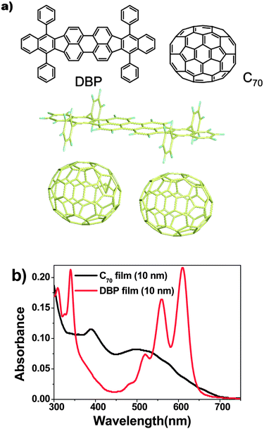 | ||
| Fig. 1 (a) (Top) Molecular structures of DBP and C70 and (bottom) aspect ratio of DBP and C70 molecules. The optimized structures of each single molecule were obtained by the B3LYP/6-31G(d) calculation. Note that this figure shows the difference in the molecular sizes, not the accurate aggregation structure in the co-deposited film. (b) Absorbance of DBP (red) and C70 (black) with a thickness of 10 nm on glass substrates. | ||
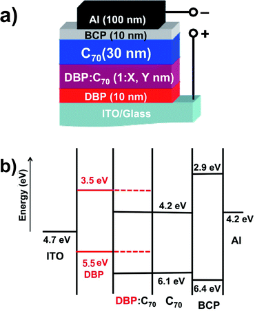 | ||
| Fig. 2 (a) Device architecture of the p–i–n photovoltaic cells, i.e. ITO/DBP (10 nm)/DBP:C70 (1:X, Y nm)/C70 (30 nm)/BCP (10 nm)/Al (100 nm) and (b) energy diagram of the photovoltaic cells. | ||
As shown in Table 1, high Jsc was observed to be >9.0 mA cm−2, when the D–A blend, i.e. the i-layer, was introduced, except for the case of 2:1 D/A ratio. A D/A ratio of 1:2 offered an optimal PCE of 5.19%. Thus we fabricated a bilayer reference cell that had the same thickness of photoactive layers, i.e. 20 nm DBP and 50 nm C70. The bilayer reference device showed Voc, short circuit current (Jsc), and FF of 0.91 V, 5.87 mA cm−2 and 67%, respectively, delivering a PCE of 3.56%. The major limitation to PCE is the relatively low Jsc of 5.87 mA cm−2. In the optimal cell having a D/A ratio of 1:2, while Voc and FF were 0.86 V and 59%, respectively, slightly lower than those of the reference cell, Jsc reached 10.26 mA cm−2. It is obvious that the 2:1 ratio based device showed very low Jsc according to Fig. 3(a), which can be ascribed to inferior carrier mobility.3
| Ratios | J sc (mA cm−2) | V oc (V) | FF (%) | PCE% |
|---|---|---|---|---|
| Bilayer | 5.87 | 0.91 | 67 | 3.56 |
| 2:1 |
4.17 | 0.89 | 47 | 1.73 |
| 1:1 |
9.31 | 0.88 | 50 | 4.08 |
| 1:2 |
10.26 | 0.86 | 59 | 5.19 |
| 1:3 |
9.87 | 0.83 | 59 | 4.78 |
| 1:4 |
9.89 | 0.86 | 56 | 4.78 |
| 1:8 |
10.02 | 0.87 | 56 | 4.85 |
| 1:16 |
9.97 | 0.87 | 49 | 4.20 |
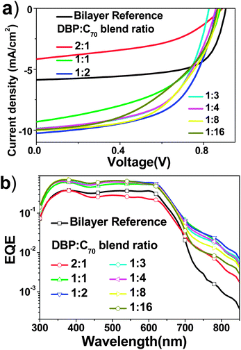 | ||
| Fig. 3 (a) J–V characteristics of the device (ITO/DBP(10 nm)/DBP:C70(30 nm)/C70(30 nm)/BCP(10 nm)/Al) with different D/A ratios under 100 mW cm−2 illumination of the AM1.5G solar spectrum. (b) Log-scale EQE of OPV devices with different D/A ratios. The bilayer reference cell has a structure of ITO/DBP (20 nm)/C70 (50 nm)/BCP (10 nm)/Al. | ||
3.2 Optical characterization
Meanwhile, molecular orientation of DBP20 and thiophene oligomers21 along the substrate surface has been studied in the neat films, providing an alternative way to maximize the resonance of light waves and the molecule by aligning the molecular plane perpendicular to the direction of light propagation. It is believed that such a molecular orientation in the horizontal direction enhances both optical and electrical properties in organic photovoltaic cells even when the films are amorphous.15Therefore VASE was used to investigate the anisotropic property of DBP and C70 co-deposited films. The refractive index and extinction coefficient of the blend films were analyzed. X-ray diffraction measurement showed no sign of any crystalline structures in both DBP neat films and the DBP:C70 blend, suggesting high accuracy of VASE data. We took the optimal ratio of 1:2 as a representative as shown in Fig. 4(a). The refractive index (n) and extinction coefficient (k) in the horizontal direction (no and ko) are higher than those in the vertical direction (ne and ke), respectively. In particular, there are two distinct anisotropies in the extinction coefficient at around 350 and 615 nm, which correspond to absorption peaks of DBP. It shows considerable horizontal orientation of DBP molecular planes even in the blend film. The rigid π-conjugated plane caused the deposited DBP film with high extinction coefficient along the direction normal to the substrates.
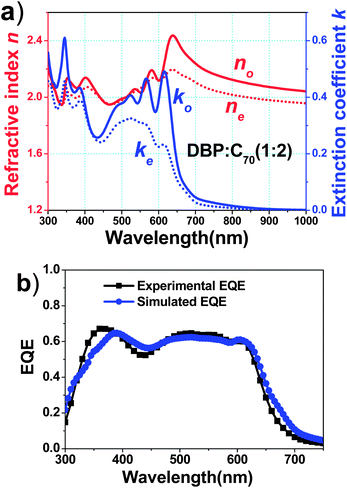 | ||
| Fig. 4 (a) Optical constants of the 1:2 DBP:C70 blend film. Red solid and dotted lines show ordinary (horizontal) and extraordinary (vertical) refractive indices (no and ne), respectively, and blue solid and dotted lines show ordinary (horizontal) and extraordinary (vertical) extinction coefficients (ko and ke), respectively. (b) Experimental and simulated EQE curves of the optimal device of ITO/DBP (10 nm)/DBP:C70 (30 nm)/C70 (30 nm)/BCP (10 nm)/Al. | ||
For comparison, anisotropic properties of series samples, including the neat DBP film and the blend films of 1:2 and 1:4, are shown in Fig. S1.† Anisotropic behaviors of the blend films are not as significant as those of the neat DBP film. no and ne have very little difference, and k values drop down dramatically in the blend films. These are mainly due to the dilution effects of C70. However it is noteworthy to point out that the ko/ke ratio at 615 nm in the blend films is still as high as that in the neat film. It indicates that the horizontal orientation of DBP molecules in the blend film is almost as good as that in the neat film. Co-deposited C70 molecules hardly disturbed the orientation of DBP ones. See Fig. S1† for further discussion.
Taking the anisotropic properties into account, we calculated EQE of the optimal device with 1:2 ratio using a reported method.20 2D absorption profiles of the OPV device under AM1.5G illumination are given in Fig. S2.† It is assumed that exciton and charge collection efficiencies are 100% in the blend film, because of complete photoluminescence quenching of DBP in the presence of C70, and negligible recombination indicated by high FF and large shunt resistance of the OPV cells. Fig. 4(b) shows the experimental and simulated EQE using no and ko data. The simulated EQE is close to the measured EQE, especially from 500 nm to 650 nm, mainly corresponding to absorption of DBP. These results show high molecular orientation in vacuum-deposited D–A blend films of OPV cells.22 Note that DBP anisotropy is still similar to that in neat DBP films. Here we address the anisotropic properties of the DBP:C70 blend films only via the VASE method. It has obvious potential, if the alignment of acceptor molecules other than fullerenes can be made for more favorable light harvesting and charge transport.15 A comprehensive work recently reported by Rand et al. explores the important role of molecular orientation in OPV cells, promoting Voc, Jsc and FF spontaneously.23
3.3 EQE and Voc with absorption of charge transfer states
EQE curves in logarithmic scale from photovoltaic cells with different D/A ratios are shown in Fig. 3(b). See linear scale EQE data in Fig. S3.† Integrating EQE with the standard AM1.5G solar spectrum yielded the calculated Jsc, which was very close to the measured Jsc under simulated solar light of AM1.5G 100 mW cm−2. Considering the absorption spectra of DBP and C70, C70 mainly absorbs blue and green light, whereas DBP covers the orange and red range.It is noted that obvious photoresponse ranging between 700 nm and 850 nm can be clearly seen from p–i–n cells with varied D/A ratios. In contrast, EQE of the bilayer device almost reached zero at 720 nm. Therefore, such photoresponse could not be simply ascribed to absorption of either donor or acceptor.
We then compared the absorption of the DBP/C70 bilayer structure and the DBP:C70 blend film on glass substrates as shown in Fig. 5(a). The absorption of 10 nm DPB (red line) is negligible beyond 700 nm, and 40 nm C70 (black line) has much weaker absorption than that of 50 nm DBP:C70 film of 1:4 ratio (green line). The difference between the two absorption curves of blend and C70 films gives rise to a broad band (blue line). Therefore it represents a new absorption, in addition to intrinsic absorption of DBP and C70.
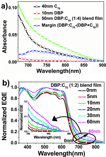 | ||
| Fig. 5 (a) Absorbance of films of C70 (40 nm, black), DBP (10 nm, red), the DBP:C70 blend film (1:4, 50 nm, green), as well as the absorbance difference between the blend film and the sum of neat C70 and DBP (blue) and (b) normalized EQE from OPV cells (ITO/DBP (10 nm)/DBP:C70 (1:2, Y nm)/C70 (30 nm)/BCP (10 nm)/Al) with different thicknesses of the i-layers. The i-layer thickness (Y nm) was changed from 0 nm to 60 nm. | ||
We chose 1:2 ratio of the blend film in p–i–n structure OPV cells to study the new absorption band, since it demonstrated strongest photoresponse in the long wavelength range among all the cells shown in Fig. 3(b). The thickness was tuned from 0 nm, i.e. a bilayer cell, up to 60 nm. The device parameters are summarized in Table 2, and J–V characteristics in light and dark states are shown in Fig. S4.† It is clear that introduction of the blend layer between the two neat layers has a dramatic influence on the device performance. Increasing the i-layer thickness results in a significant increase in Jsc and reduction in FF. Improvement of Jsc comes from absorption of the i-layer. However, FFs decrease dramatically from 69% to 49%, because the i-layer has carrier mobilities lower than those in the neat films, and hence charge recombination becomes more severe. As indicated in Fig. S4(a),† in the fourth quadrant where the cells approach the flat band condition, i.e. Voc, charge collection becomes very sensitive to bias voltage. When the thicknesses of the i-layer are 5 nm and 10 nm, the increase in Jsc is not sufficient to compensate the loss in FF. PCE thus dropped down compared to that of the bilayer device. Jsc then took the role to enhance PCE dramatically, when the thicknesses of the blend films were 20 nm and 30 nm. For the device having 30 nm thick blend layer, Jsc, in comparison to that of the planar heterojunction cell, was improved by over 50%, which was attributed to absorption and exciton collection of the blend film.5 Meanwhile, the FF of the device decreased by about 20%, which is attributed to the charge carrier recombination in the blend film.24 Then, PCE decreased when the thickness of the blend film reached 60 nm.
| X (nm) | PCE% | J sc (mA cm−2) | FF (%) | V oc (V) | J 0 (mA cm−2) | n |
|---|---|---|---|---|---|---|
| 0 | 4.16 | 6.70 | 69 | 0.91 | 2.23 × 10⁻¹¹ | 1.38 |
| 5 | 3.97 | 6.85 | 64 | 0.90 | 7.09 × 10⁻¹⁰ | 1.59 |
| 10 | 4.04 | 7.83 | 58 | 0.88 | 1.37 × 10⁻⁸ | 1.85 |
| 20 | 4.53 | 9.13 | 56 | 0.89 | 8.71 × 10⁻⁹ | 1.78 |
| 30 | 5.19 | 10.26 | 59 | 0.86 | 1.68 × 10⁻⁸ | 1.65 |
| 60 | 3.49 | 9.39 | 43 | 0.86 | 2.62 × 10⁻⁸ | 1.89 |
Normalized EQE data in Fig. 5(b) show a clear trend that the photoresponse in the long wavelength range increases with the thickness of the blend film. See real EQE data given in Fig. S5.† Considering the additional absorption band revealed in Fig. 5(a), we confirmed that the photoresponse lower than the bandgap of photoactive materials is due to the formation of charge transfer states between DBP and C70. On one hand, the charge transfer absorption contributes to photocurrent by ∼5%. On the other hand, it should be addressed that Voc decreases because of the insertion of the blend films, and varies with the blending ratio, as summarized in Tables 1 and 2.
From Table 1, a Voc of 0.91 V was observed from the reference cell, while Voc was reduced for all p–i–n photovoltaic cells. With increasing the thickness of the i-layers from 0 nm to 60 nm, Voc decreases from 0.91 V to 0.86 V. In such p–i–n cells, only the thickness of the blend films was changed, while the electrical contacts essentially remained the same. It is well-known that Voc is determined by the offset between HOMO of the donor and LUMO of the acceptor.25 However in our case, absorption of charge transfer states in the blend films shall be responsible for the reduction in Voc.
The relationship between charge transfer absorption and Voc can also be seen from EQE data in Fig. 3(b). The curves in log scale suggest that there is an optimal blend ratio for the formation of charge transfer states. From the 1:2 cell, we observed both strong photoresponse in long wavelength, and relatively low Voc. The cell based on 1:16 ratio has little photoresponse in the same range, though its PCE is still competitive.26 These results indicate that sufficient contact between DBP and C70 molecules enables effective formation of charge transfer states.
3.4 Electrical analysis
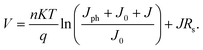
It has been well known that charge transfer states are formed between donor and acceptor molecules, following the exciton separation at the D–A interface. Such states play an important role in determining free carrier generation and Voc.27–30 In our case, the charge transfer states form at the ground state level and give rise to absorption below the bandgaps of DBP and C70, meaning a new species appears. It also influences electrical properties of the photovoltaic cells.31 We now turn to the diode equation to understand why and how Voc changes.32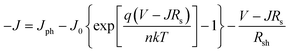 | (1) |
 | (2) |
Considering Jph = 0 in the dark state, J0 was then derived via fitting the dark J–V curves using eqn (2), and the resulting values are listed in Table 2. J0 of the reference cell is 2.23 × 10⁻¹¹ mA cm−2, and 5 nm blend film boosts J0 up by more than 1 order of magnitude. Further increase of the blend film thickness results in larger J0 on the order of 10−8 mA cm−2. It can be clearly seen that J0 increased with the thickness of the i-layer, suggesting that the increase in J0 is associated with the formation of charge transfer states.
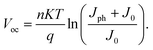
According to the correlation between Voc and J0:33
 | (3) |
It shows that when J0 increases, Voc should decrease. Since the thickness of blend films influences J0, and then J0 affects Voc, the correlation between the thickness of the i-layer and Voc becomes clear.
The charge transfer absorption in the long wavelength range actually narrows down the effective bandgap of the heterojunction.25,34,35 It could be a possible reason for reduction of Voc. Such a bandgap shrinking normally occurs in inorganic semiconductors at elevated temperatures.36 The concentration of thermal activated carriers increases with temperature. It causes increase in J0, i.e. the number of carriers that can be swept out under reverse bias at equilibrium, and intensifies the recombination of minority carriers under light illumination. As a result, Voc decreases.
In the case of organic planar heterojunctions, the effective bandgap is determined by the photoactive materials. For the bilayer reference cell, the interface between the donor and acceptor plays a minor role due to limited D–A contact. Voc is determined by the difference between HOMO of the donor and LUMO of the acceptor.37 In the i-layer of p–i–n cells, donor and acceptor molecules are mixed such that the D–A intermolecular interaction becomes strong, triggering formation of charge transfer states, and thus decrease of the effective bandgap. It then causes strong thermal activated electron transition, which is responsible for increase of J0. Hence, Voc from D–A blend films deviates from the HOMO–LUMO difference.38,39
4. Conclusions
In summary, we demonstrated high-efficiency photovoltaic devices based on DBP/C70 heterojunctions. A p–i–n architecture was introduced for enhancing light harvesting and thus PCE. The effects of the D–A blend layer are discussed in terms of optical and electrical properties of the photovoltaic cells. We found horizontal orientation of DBP molecules even in blend films, which provides us with a potential approach for improving light harvesting. Strong absorption of charge transfer states was observed in the D–A blend films. It contributes to Jsc, and meanwhile induces high J0 and thus Voc loss in D–A blend heterojunctions. Therefore the paradox roles of the charge transfer states should be considered in the design of materials and devices for OPV cells.Acknowledgements
This project is sponsored under the Japan Science and Technology Agency (JST) via the Japan Regional Innovation Strategy Program by the Excellence (J-RISE), and Dissemination of Tenure Tracking System Program of Ministry of Education, Culture, Sports, Science and Technology, Japan. This work is also partly supported by Mazda Foundation. We also thank the Research Center for Computational Science (RCCS), Okazaki National Research Institutes for the use of a SGI Altix4700 computer.Notes and references
- N. S. Sariciftci, L. Smilowitz, A. J. Heeger and F. Wudl, Science, 1992, 258, 5087 Search PubMed.
- C. W. Tang, Appl. Phys. Lett., 1986, 48, 183 CrossRef CAS.
- P. Peumans, A. Yakimov and S. R. Forrest, J. Appl. Phys., 2003, 93, 3693 CrossRef CAS.
- G. Ruani, C. Fontanini, M. Murgia and C. Taliani, J. Chem. Phys., 2002, 116, 1713 CrossRef CAS.
- M. C. Scharber, C. Lungenschmied, H.-J. Egelhaaf, G. Matt, M. Bednorz, T. Fromherz, J. Gao, D. Jarzabd and M. A. Loi, Energy Environ. Sci., 2011, 4, 5077 RSC.
- D. Cao, M. Amelia, L. M. Klivansky, G. Koshkakaryan, S. I. Khan, M. Semeraro, S. Silvi, M. Venturi, A. Credi and Y. Liu, J. Am. Chem. Soc., 2010, 132, 1110 CrossRef CAS.
- Y. P. Yi, V. Coropceanu and J. L. Brédas, J. Am. Chem. Soc., 2009, 131, 15777 CrossRef CAS.
- J. L. Brédas, J. Norton, J. Cornil and V. Coropceanu, Acc. Chem. Res., 2009, 42, 1691 CrossRef CAS.
- G. Yu, J. Gao, J. C. Hummelen, F. Wudl and A. J. Heeger, Science, 1995, 270, 1789 CrossRef CAS.
- M. Hiramoto, H. Fujiwara and M. Yokoyama, Appl. Phys. Lett., 1991, 58, 1062 CrossRef CAS.
- J. Drechsel, B. Männig, F. Kozlowski, M. Pfeiffer, K. Leo and H. Hoppe, Appl. Phys. Lett., 2005, 86, 244102 CrossRef.
- K. Walzer, B. Maennig, M. Pfeiffer and K. Leo, Chem. Rev., 2007, 107, 1233 CrossRef CAS.
- (a) J. G. Xue, B. P. Rand, S. Ushida and S. R. Forrest, Adv. Mater., 2005, 17, 66 CrossRef CAS; (b) Z. R. Hong, B. Maennig, R. Lessmann, M. Pfeiffer, K. Leo and P. Simon, Appl. Phys. Lett., 2007, 90, 203505 CrossRef.
- R. Fitzner, C. Elschner, M. Weil, C. Uhrich, C. Koerner, M. Riede, K. Leo, M. Pfeiffer, E. Reinold, E. Mena-Osteritz and P. Baeuerle, Adv. Mater., 2012, 24, 675 CrossRef CAS.
- (a) D. Yokoyama, J. Mater. Chem., 2011, 21, 19187 RSC; (b) D. Yokoyama, A. Sakaguchi, M. Suzuki and C. Adachi, Org. Electron., 2009, 10, 127 CrossRef CAS.
- (a) D. Fujishima, H. Kanno, T. Kinoshita, E. Maruyama, M. Tanaka, M. Shirakawa and K. Shibata, Sol. Energy Mater. Sol. Cells, 2009, 93, 1029 CrossRef CAS; (b) M. Hirade and C. Adachi, Appl. Phys. Lett., 2011, 99, 153302 CrossRef.
- J. Sakai, T. Taima, T. Yamanari and K. Saito, Sol. Energy Mater. Sol. Cells, 2009, 93, 1149 CrossRef CAS.
- G. Chen, H. Sasabe, Z. Q. Wang, X. F. Wang, Z. R. Hong, Y. Yang and J. Kido, Adv. Mater., 2012, 24, 2768 Search PubMed.
- M. Riede, C. Uhrich, J. Widmer, R. Timmreck, D. Wynands, G. Schwartz, W. Gnehr, D. Hildebrandt, A. Weiss, J. Hwang, S. Sundarraj, P. Erk, M. Pfeiffer and K. Leo, Adv. Funct. Mater., 2011, 21, 3019 CrossRef CAS.
- D. Yokoyama, Z. Q. Wang, Y. J. Pu, K. Kobayashi, J. Kido and Z. R. Hong, Sol. Energy Mater. Sol. Cells, 2012, 98, 472 Search PubMed.
- D. Wynands, M. Erber, R. Rentenberger, M. Levichkova, K. Walzer, K.-J. Eichhorn and M. Stamm, Org. Electron., 2012, 13, 885 Search PubMed.
- C. Schünemann, D. Wynands, L. Wilde, M. P. Hein, S. Pfützner, C. Elschner, K.-J. Eichhorn, K. Leo and M. Riede, Phys. Rev. B: Condens. Matter Mater. Phys., 2012, 85, 245314 Search PubMed.
- B. P. Rand, D. Cheyns, K. Vasseur, N. C. Giebink, S. Mothy, Y. Yi, V. Coropceanu, D. Beljonne, J. Cornil, J.-L. Brédas and J. Genoe, Adv. Funct. Mater., 2012, 22, 2987 Search PubMed.
- Y. Zhang, X. D. Dang, C. Kim and T. Q. Nguyen, Adv. Energy Mater., 2011, 1, 610 Search PubMed.
- M. C. Scharber, D. Wuhlbacher, M. Koppe, P. Denk, C. Waldauf, A. J. Heeger and C. J. Brabec, Adv. Mater., 2006, 18, 789 CrossRef CAS.
- M. L. Zhang, H. Wang, H. K. Tian, Y. H. Geng and C. W. Tang, Adv. Mater., 2011, 23, 4960 Search PubMed.
- K. Vandewal, K. Tvingstedt, A. Gadisa, O. Inganas and J. V. Manca, Nat. Mater., 2003, 8, 904 Search PubMed.
- D. Veldman, S. C. J. Meskers and R. A. J. Janssen, Adv. Funct. Mater., 2009, 19, 1939 CrossRef CAS.
- C. Deibel, T. Strobel and V. Dyakonov, Adv. Mater., 2010, 22, 4097 CrossRef CAS.
- P. E. Keivanidis, V. Kamm, C. D. Smith, W. Zhang, F. Laquai, I. McCulloch, D. D. C. Bradley and J. Nelson, Adv. Mater., 2010, 22, 5183 CrossRef CAS.
- K. Akaike, K. Kanai, Y. Ouchi and K. Seki, Adv. Funct. Mater., 2010, 20, 715 CrossRef CAS.
- B. P. Rand, D. P. Burk and S. R. Forrest, Phys. Rev. B: Condens. Matter Mater. Phys., 2007, 75, 115327 CrossRef.
- W. J. Potscavage, Jr, S. Yoo and B. Kippelen, Appl. Phys. Lett., 2008, 93, 193308 CrossRef.
- A. Gadisa, M. Svensson, M. R. Andersson and O. Inganas, Appl. Phys. Lett., 2004, 84, 1609 CrossRef CAS.
- K. Vandewal, A. Gadisa, W. D. Oosterbaan, S. Bertho, F. Banishoeib, I. V. Severen, L. Lutsen, T. J. Cleij, D. Vanderzande and J. V. Manca, Adv. Funct. Mater., 2008, 18, 2064 CrossRef CAS.
- J. Nelson, The Physics of Solar Cells, ISBN 1-86094-340-3, Imperial College Press, London, UK, 2003 Search PubMed.
- C. J. Brabec, A. Cravino, D. Meissner, N. S. Sariciftci, T. Fromherz, M. T. Rispens, L. Sanchez and J. C. Hummelen, Adv. Funct. Mater., 2001, 11, 374 CrossRef CAS.
- K. Tvingstedt, K. Vandewal, A. Gadisa, F. L. Zhang, J. Manca and O. Inganas, J. Am. Chem. Soc., 2009, 131, 11819 CrossRef CAS.
- G. Garcia-Belmonte and J. Bisquert, Appl. Phys. Lett., 2010, 96, 113301 CrossRef.
Footnote |
| † Electronic supplementary information (ESI) available. See DOI: 10.1039/c2ee22952h |
| This journal is © The Royal Society of Chemistry 2013 |