Optofluidic devices and applications in photonics, sensing and imaging†
Lin
Pang
*,
H. Matthew
Chen
,
Lindsay M.
Freeman
and
Yeshaiahu
Fainman
*
Jacobs School of Engineering, University of California, La Jolla, California 92093-0407, San Diego. E-mail: lpang@ece.ucsd.edu; fainmain@ece.ucsd.edu.; Fax: 1-858-534-1225; Tel: 1-858-534-7208
First published on 1st June 2012
Abstract
Optofluidics integrates the fields of photonics and microfluidics, providing new freedom to both fields and permitting the realization of optical and fluidic property manipulations at the chip scale. Optofluidics was formed only after many breakthroughs in microfluidics, as understanding of fluid behaviour at the micron level enabled researchers to combine the advantages of optics and fluids. This review describes the progress of optofluidics from a photonics perspective, highlighting various optofluidic aspects ranging from the device's property manipulation to an interactive integration between optics and fluids. First, we describe photonic elements based on the functionalities that enable fluid manipulation. We then discuss the applications of optofluidic biodetection with an emphasis on nanosensing. Next, we discuss the progress of optofluidic lenses with an emphasis on its various architectures, and finally we conceptualize on where the field may lead.
 Lin Pang | Lin Pang is a research scientist in the Department of Electrical and Computer Engineering, University of California, San Diego. He received his Ph.D. degree from Sichuan University, Sichuan, China, in 1998. His current interests include hybrid holographic lithography, nanofabrication, micro, nanofluidics, and sensing based on coupled plasmonic nanoresonators. |
 H. Matthew Chen | Haiping Matthew Chen received his Master’s degree from the University of Illinois, Urbana-Champaign. Currently, he is completing his Ph.D. in electrical engineering at the University of California, San Diego. His interests include computer simulations of plasmonic and optofluidic phenomena and fabrication and characterization of plasmonic nanostructures for biological sensing applications. Presently, he is also with Navair working on defense microwave and photonic applications. |
 Lindsay M. Freeman | Lindsay M. Freeman received the B.S. degree in chemical engineering from the University of Southern California, Los Angeles, in 2010. She is currently working towards her Ph.D. degree in chemical engineering at the University of California, San Diego, under the supervision of Prof. Y. Fainman. |
 Yeshaiahu Fainman | Y. Fainman is a Cymer Professor in ECE at the University of California, San Diego. He is directing the Ultrafast and Nanoscale Optics Group and has made pioneering contributions to near field optical phenomena, inhomogeneous and meta-materials, nanophotonics and plasmonics, optofluidics and non-conventional imaging. The research applications target information technologies and biomedical sensing. He is a Fellow of the OSA, Fellow of the IEEE, Fellow of the SPIE, and recipient of the Miriam and Aharon Gutvirt Prize, Lady Davis Fellowship, Brown Award and Gabor Award. He has contributed to over 200 manuscripts in peer review journals and over 350 conference presentations and conference proceedings. |
1. Introduction
Optofluidics, as described in the name, is the emerging field of integrating photonics with fluidics. Although liquid enabled optical devices, such as the liquid mirror telescope1 or dye lasers,2 were invented a long time ago, the terminology of optofluidics, which refers to the ability to manipulate fluid at the chip scale, was formally adopted only after successes in the area of microfluidics with extensive efforts by optical and microfluidic groups worldwide.3–14 Microfluidics provides researchers with the ability to exploit its small size and laminar flow characteristics in microchannels. A revolutionary material is polydimethylsiloxane (PDMS) which is used to make optically transparent microfluidic components. Due to its polymeric, elastic property and accompanied soft-lithography capability, it is the perfect exploratory research platform. Its integrated valves,3–8 mixers9,10 and pumps4,11 combined with fluidic channels resulted in microfluidic chemical factories on a chip.Optical devices are channels whose materials interact with light and result in the alteration of the light path. Snell's law, or more precisely Maxwell's equations, governs the outcome of the interactions. In optical devices, the refractive index describes the material property that directly affects how light interacts with the different media, such as the degree in which light would be reflected, transmitted, or absorbed. In other words, the distribution of the refractive indices of the media would control how the light passes through the media, resulting in components such as lens, mirrors, waveguides, etc.
The dependence of the behaviour of light on the index distribution affects the performance if the index distribution varies. When fluidic control matured to the extent of on-chip configuration, the marriage between optics and fluidics rapidly occurred. The term “optofluidics” was coined in 2004 to reflect a newly formed research initiative supported by the Defence Advanced Research Projects Agency (DARPA) of the U.S. Department of Defense.13,14 Since then, optofluidics has become one of the most active research areas with publications increasing exponentially.15–18 Optofluidic devices have evolved substantially from controlling a device's property via flow or optical manipulations to revolutionary applications in both sensing and imaging.
In this review, after briefly reviewing the background on microfluidics, we will summarize optofluidic devices in terms of their functionalities: property manipulation, sensing, and imaging. Readers will witness the development of the field, starting with a discussion of optofluidic devices controlled by flow, to an overview of liquid photonics. This review will emphasize the inter-disciplinary applications created by optofluidics, leaving readers amazed by the potentials of this promising research field.
2. Background on microfluidics
Throughout this review, there are two separate terms we are using: fluid and liquid. Without further mention, we will refer to fluid as a liquid. One important property for fluids is Pascal's law, which states that when there is an increase in pressure at any point in a confined fluid, there is an equal increase at every other point in the container. Hydraulic lift is a direct result of Pascal's law, in which a large amount of power can be transferred through small tubes and flexible hoses. This property is preserved at the microscale, as Quake3,4 demonstrated with the pneumatic valves integrated in a PDMS elastomer chip, fabricated by applying the soft lithography technique proposed by Whitesides.19 PDMS is a soft silicon-based organic polymer that is optically transparent from 240 nm to the near infrared spectral region. Its transparency and low auto-fluorescence allow for optical transmission and detection over the entire visible spectrum. Another advantage is the easiness of fabrication: in soft lithography, PDMS is used as a cast to harden on a patterned photoresist master. The photoresist is then removed to leave behind channels. Microfluidic channels can then be formed by bonding a cover layer. Many easy bonding approaches have been developed to simplify the process,20 including utilizing a hydrophobic, conformal contact of two fully cured layers of PDMS that result in a reversible seal.21 Fully cured PDMS can be activated by oxygen plasma and bonded to another fully cured PDMS layer or to other material such as glass slides.22,23 Partial curing of PDMS can also be used as an effective, inexpensive method for creating multi-layer devices.24 The pneumatic valves are made with multiple patterned layers of elastomer to create three-dimensional channels via multilayer soft lithography.8 The membrane of a polymer between the channels is engineered to be relatively thin. When pressure is applied to the lower channel (control channel), the membrane deflects upward to close the flow of the upper channel (flow channel), as shown in Fig. 1(a).3 Using the same principle, solution mixers and pumps can be constructed on the PDMS chip as shown in Fig. 1(b)11 and 1(c).4 The introduction of on-chip hydraulic controls paved the way for on-chip, high-throughput microfluidics for fast turnaround of exploratory novel concepts, leading to thousands of individually controlled channels for protein detection and DNA sequencing.5 These basic microfluidic components are the building blocks of microfluidics and were the prerequisites for the emergence of optofluidics.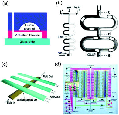 | ||
| Fig. 1 Microfluidic devices made from PDMS; (a) push-up valves; (b) mixer; (c) pump; (d) integrated system. Part (a) is adapted from ref. 3; part (b) from ref. 11, with permission from the American Institute of Physics. Part (c) and (d) are adapted from ref. 4 and 5, respectively, with permission from AAAS. | ||
In microfluidics, viscous forces become more important than inertial forces, resulting in fluids that do not mix convectively when they meet in a microchannel, but rather will flow in parallel. The only mixing that occurs is the result of diffusion across the interface between two fluids. This laminar flow property preserves refractive index contrast and index distributions in PDMS microchannels, providing a series of special functionalities that have aided the development of novel optofluidic devices.
3. Photonics
The success in microfluidics provides optical engineers the materials or processes that can be employed to adjust optical responses by using the already developed flow control in an on-chip fashion.3.1 Optofluidic switch
One of the advantages of fluids is that the indices can be altered by changing the fluids in order to modify the optical responses of the devices. An optofluidic switch is a typical example, where substituting one fluid for another completely changes the light path, as shown in Fig. 2. In this case, the optofluidic switch is enabled by switching between the transmission and the total internal reflection with two fluids of low and high indices flowing through the mirror channel.25 The device, shown schematically in Fig. 2(a), has two distinct layers of microchannels separated by thin flexible membranes in the regions where they overlap. The first layer, the flow layer, contains the main functional element of the device – a flat parallel mirror channel (pink area in Fig. 2(b)). It can be filled with either pure water with an index of 1.33 from inlet 1 (enabling the light incident from the PDMS to be totally reflected) or an index matching salt solution with an index of 1.41 from inlet 2 (enabling the light to be transmitted), see Fig. 2(c) and 2(d). The channels connecting the inlets and the outlet can be completely sealed by the flexible membranes, which serve as pressure-actuated and integrated “push-up” valves.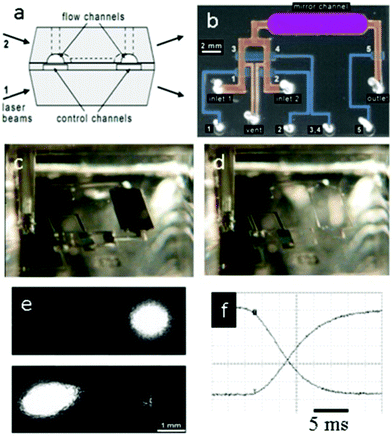 | ||
| Fig. 2 (a) Schematic drawing of the three-layer elastomer chip with four optical quality facets. (b) Microphotograph of the switch device. (c) Microphotograph showing the mirror channel reflecting the light with water running through; (d) Light goes through the mirror channel with index matching fluid filling the channel. (e) Images of the bypass mode (upper) and exchange mode (down); (f) Power of transmitted and reflected beams as a function of time. Part (a), (b) and (e) are produced from ref. 25 with permission from the American Institute of Physics. | ||
Fig. 2(c) shows the mirror channel filled with water for total reflection, while Fig. 2(d) shows the channel filled with index matching solution for transmission. Fig. 2(e) shows the transmitted (upper) and reflected (bottom) beam spots captured on a CCD camera. Fig. 2(f) shows the time response of the switch with a control channel pressure of 15 psi, corresponding to roughly 10 ms switching speed. The switching speed depends on the flow rate, which depends on the dimension of the channel, pressure difference and the viscosity of the flow. Increasing the pressure difference and the channel height while reducing the channel length are potential approaches to increasing the switching speed. Fig. 2(e) also shows the crosstalk, which was caused by the index mismatch. This phenomenon could be used to make an optofluidic variable attenuator by controlling the reflectivity of the fluid–PDMS interface while adjusting the index in the mirror channel.26 This configuration can also be used to determine the index value by measuring the reflected power.
Following the same principle, a waveguide-based, on-chip light routing optofluidic switch is achieved with a tunable air-gap mirror, by which the light is deflected via total internal reflection in the bypass state.27
The optical beam switch can also be achieved based on diffraction from a blazed grating when different fluids flow over it. The diffracted angles are proportional to the mismatch between the refractive indices of the material of the grating and the liquid in the channel.28 Optical switching was also achieved in the in-plane liquid-core/liquid-cladding (L2) waveguides by flow rate manipulations29 and pneumatic control.30
Unlike the abrupt index shift of previously discussed examples, the optical response can be precisely manipulated by fine tuning the required fluidic index by mixing two fluids with any concentration, generating a range of refractive indices between the two initial fluids. A fine tuning of an optical microring resonator device (MRD) by dynamic variation of the refractive index of the medium surrounding the waveguides was demonstrated by manipulating the upper cladding of the solid MRD waveguides.31 This fine tuning of the refractive index of fluids can also be employed in the fine tuning of the surface plasmonic polariton (SPP) mode to achieve designed SPP interaction.32
3.2 Optofluidic laser
The laminar flow nature of microfluidics enables two fluids to flow in parallel without convection, which was employed to make a novel liquid-core/liquid-cladding waveguide.29 The liquids are introduced into the channel of a microfluidic network side-by-side to sandwich the flowing high index core liquid between flowing slabs of the low index cladding fluid. Manipulating the rate of flow and the composition of the liquid can tune the characteristics of the optical system. On the other hand, the smooth interface between the liquid–liquid interface greatly reduces optical scattering loss. When an optical cavity is built on the ends of the waveguide and fluorescent dye is used as a core medium, L2 lasing is achieved. As shown in Fig. 3(a),33 the active region is terminated at both ends with T-junctions, which were coated with thin layers of gold to act as mirrors for the optical cavity. A linewidth of 4 nm was achieved with 16 uJ pump power. This linewidth of a few nanometers implies that the multiple lasing modes or the amplified spontaneous emission is due to poor transverse mode confinement and longitudinal mode selection. The transverse single-mode waveguide mode can be achieved with an L2 waveguide by forming a small core using pressure-driven flow and adjusting the index contrast between the core and cladding fluids. For the longitudinal mode selection, Tang et al. described a microfluidic droplet dye laser with whispering gallery modes, enabling a linewidth of 0.3 nm.34 This laser was based on a train of alternating droplets (20–40 μm in diameter) containing solutions of different dyes – each capable of lasing at a different wavelengths – suspended in a fluorocarbon carrier liquid in a PDMS microchannel, as shown in Fig. 3(b). These drops flow through a region where the dyes in the drops are excited optically, one at a time, and lase, capable of switching at frequencies up to 3.6 kHz. This technique was extended to continuously adjust the wavelengths of lasing by exciting different sizes of micro drops in the channel.35 Using two liquids that were partially miscible with each other, they enable a series of dye-doped droplets with continuously decreasing radius in a microfluidic channel. The wavelength of emission can be tuned from 700 to 620 nm as the radius of the drops decreases from 21 μm to 7 μm.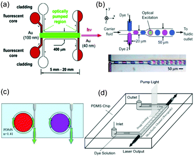 | ||
| Fig. 3 (a) Schematic drawing of the liquid-core/liquid-cladding waveguide laser. (b) Whispering gallery mode laser from droplets. (c) Liquid-core/solid-cladding micro ring laser. (d) Distributed feedback laser of solid-core/liquid-cladding wavequide. Part (a) is produced from ref. 33 with permission from American Chemical Society. Part (b) is adapted from ref. 34. Part (c) and (d) are produced from ref. 37 and 41, respectively, with permission from the Optical Society of America. | ||
On the other hand, the liquid core/solid cladding or solid core/liquid cladding waveguide based lasing configurations proved to be alternatives for mode selections. Li et al.36 and Suter et al.37 used a microring as a liquid core and PDMS as the cladding and demonstrated a single mode liquid-core waveguide based microring cavity, as shown in Fig. 3(c).37 A glass capillary based micro-bubble38 and a micro-ring laser39 were also demonstrated; additional work exhibited lasing based on Forster resonance energy transfer of gain medium with labeled DNA.40 A feedback distributed grating in solid core/liquid cladding configuration was also employed to select a longitudinal lasing mode. Fig. 3(d) shows a typical feedback distributed optofluidic laser.41 The laser cavity consists of a single mode liquid core/PDMS cladding channel waveguide and a phase shifted 15th order distributed feedback (DFB) structure. Its wavelength can be continuously tuned over a large range with a simple mechanical deformation.42 Similarly, a solid circular distributed feedback grating with a dye solution acting as the cladding layer was demonstrated by Song et al.43 These optofluidic dye lasers will have great potential for highly parallel multiplexed on-chip spectroscopic applications.
3.3 Optofluidic waveguide for microelectronics
Besides employing fluid as a control, dielectric, or active medium as reviewed above, fluid can also be used as a nonlinear material. Full optical switching was demonstrated using stimulated Raman excitation through liquid in a hollow optical fiber,44 where the long interaction length of about one meter was used for signal generation. In microfluidics, the material used for fabricating microfluidic channels is usually PDMS, whose optical transparency, soft lithography capability and its ability to support pneumatic controllers (valves, pump, etc.) have made it an excellent and indispensible material for exploratory research in fluidic systems, especially for bio-research and bioengineering. However, PDMS's chemical durability, mechanical and thermal stability make it incompatible with microelectronic systems, where complementary-metal-oxide-semiconductor (CMOS) compatible materials and processing are required. Dumais et al.45 proposed a plasma-enhanced chemical vapor deposition (PECVD) assisted method, as shown in Fig. 4(a). The high refractive index (nD = 1.46) PECVD processed cladding cannot be used for a low index liquid core. Antiresonant reflecting optical waveguides (ARROWs) were proposed to use low index core material by designing the anti-resonant Fabry-Pérot reflector, as shown in Fig. 4(b).46 The optical mode in ARROW is leaky, but relatively low-loss propagation can be achieved by making the Fabry-Pérot reflector. The multiple dielectric layers are deposited on the sacrificial layer in the fabrication process. For long waveguide configurations, where the curved format is preferred for smaller area, the satisfaction of the Fabry–Pérot condition on the bending area would be an issue.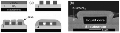 | ||
| Fig. 4 (a) Process to form embedded microchannels in n-borophosphosilicate glass; (1) PECVD of template layer, (2) formation of template ridges-photolithography RIE, (3) PECVD of BPSG, (4) high-temperature anneal to form microchannels. (b) ARROW waveguide cross section consisting of SiN and SiO2 dielectric layers and a liquid core. Part (a) is adapted from ref. 45 with permission from Optical Society of America. Part (b) is reproduced from ref. 46 with permission from the American Institute of Physics. | ||
The low index core configuration enables the solution to operate at a single optical waveguide mode, which will find many applications in bioengineering where aqueous based environments are desired.
4. Sensing
Optofluidic based sensing methods have recently gained significant attention as described in recent comprehensive reviews.47,48 Two of the commonly reported metrics of a sensor are the sensitivity (S) and limit of detection (LOD). S refers to the response of the sensor output signal to the unit change of a sensor parameter, e.g. refractive index unit for refractive index sensor. LOD refers to the minimum detectable change, usually concentration of the measurand. Optofluidic sensors are detecting the response of the interaction between the optical field and bioreagents of interest in the environment. Therefore, increasing the overlap between the optical field and target molecules is the ultimate way to improve the sensitivity of the sensing configurations, while improving the signal to noise ratio would be an effective way to increase the limit of detection. Unlike fluorescence or interference49,50 based sensors, optical resonance plays a big role in label-free sensing. These optical biosensors include dielectric resonators (rings or disks),51 Fabry–Perot resonators,52 photonic crystals,53 surface plasmon resonances, etc. This review only focuses on the plasmonic based sensors.Plasmonic sensing is used mainly due to its high sensitivity, which results from the fact that the maximum optical field is confined to the surface, where the biological binding reactions take place. Surface plasmon polariton (SPP) is the surface charge density oscillation, a consequence of the coupling between a photon and free electrons on the interface of a metal and dielectric. Due to the momentum mismatch, SPP waves cannot be excited by direct illumination of light,54 but by (1) prism coupling via attenuated total reflection (Kretschmann configuration) or by (2) a diffractive grating. Surface plasmon resonance (SPR) was first introduced for sensing by Nylander and Liedberg.55 Since then, due to its real-time analysis of biospecific interactions without the use of labeled molecules, SPR sensing has continued to improve the sensor designs, sensing surface characterizations,56 and further sensor commercialization.57 In 1998, Ebbesen et al. reported the observation of enhanced transmittance through optically thick metallic films with subwavelength features.58 Since then, Brolo et al. demonstrated the use of subwavelength hole arrays for sensing applications.59 Different interrogation approaches have been explored, such as incident angle,60 intensity,61 polarization,62 as well as multiple modes.63
Although SPR based sensing's highest sensitivity results from maximum field confinement at the surface, the high propagation loss of a metal surface heavily damps the resonance, leading to a broader resonant linewidth compared with its dielectric counterparts. The broader linewidth of the SPR makes the small resonant shift undetectable. Two orthogonally aligned polarizers sandwiching the nanohole substrate were employed to filter out the directly transmitted nonresonant background and changed the SPR from a Fano shape to a Lorentzian shape.60 The resonant linewidth was reduced from 5.5 nm to 2.5 nm from parallel (PP) to orthogonal polarizer-analyzer (OP), as shown in Fig. 5(a). This improvement of signal-to-noise ratio enhances the LOD. Enhancement of sensitivity was also conducted by coupling localized surface plasmonic resonators (LSPR) with propagating SPR. As shown in Fig. 5(b), there is a layer of gold film on top of a perforated substrate, in which the film protrudes out, forming nanovoids. The coupling between the propagating SPR and LSPR enhances the amplitude of the electric field, as shown in Fig. 6(b). The field penetration depth decreased, leading to surface sensitivity enhancement.64
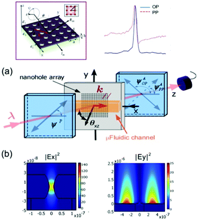 | ||
| Fig. 5 Surface Plasmon Resonance (SPR) based detection (a). Conceptual diagram of the 2D nanohole-array-based SPR sensor. (b) Near-field intensity distribution of the electric field on the nanoresonant substrate resulted from coupling between LSPR and SPR in a 2D metal film perforated with nanohole. Adapted from ref. 60 and 64, copyright 2006, 2009 Optical Society of America. | ||
 | ||
| Fig. 6 a) SEM of fabricated upward nanoresonator with opening of 50 nm. b) A sample uniformity plot of 5 nanotorches at different locations within the same substrate. | ||
The interrogation area of a propagating SPR based sensor is tens of microns. Nanoparticle or nanoresonator based SPR sensors were also explored, including a nanoparticle array65 and a random nanohole array.66 A single nanoparticle based sensor was demonstrated in a hydrogen sensor at the single-particle level.67 The single nanoresonator based sensor avoids any statistical effects, possibly enabling low LOD detections.
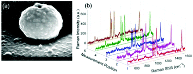
The sensitivity of the nanosensor depends on the strength of the local field. Coupled nanoresonant designs were applied to enhance the local field by almost one order of magnitude,68,69 but the resolution requirement makes them difficult to be fabricated by current top-down nanofabrication approaches with electron beam and focused ion beam lithography. Bottom-up methods were employed to make a nanocrescent resonator shape,70,71 where coupling among nanotip to nanotip (edge–edge), tip–nanocavity, and nanocavity–nanobody were demonstrated. The random orientation of 3D nanocrescent was overcome to produce reproducible nanoresonators, as shown in Fig. 6. The reproducibility of 80%, on par with standard commercial surface enhanced Raman scattering substrate, was verified by measuring different single nanoresonators within the same substrate.72
In optofluidic sensors, the mass transport of the target molecule on the sensing area directly affects the detection speed. For most sensing platforms, recognition molecules are immobilized on the sensing surface, and fluid delivers the target molecule through the channel over the surface. Due to the laminar flow nature of microfluidics, the flow rate at the surface is zero, and target molecules are not delivered convectively, but diffuse to the surface to bind with their recognition molecules. Commercial microfluidic systems use interval injections of fluid and air to improve the mass transport.73 Flow through microfluidics was introduced for both a plasmonic sensor74 and photonic crystal sensor,75 in which the substrate is back-etched so that the liquid could flow through the metal or dielectric membrane. Orders of enhancement in the mass-transport rate were demonstrated compared to the traditional flow-over method.
5. Imaging
Fluid can adjust the optical path length or focal length, enabling adaptive operation by changing the medium of the lens. The reconfigurability of the optofluidic lens can be applied in many areas, including lab-on-chip integration, autofocusing feature on a cell phone camera, vision autocorrection, etc.The lens' focusing power is determined by its index gradient, which can be manipulated by controlling the shape, curvature or index difference of the lens. Optofluidic lenses were first designed with a chamber covered by a flexible membrane, which deforms when a pressure is applied to pump the liquid in and out of the chamber. The pressure in the chamber changes the curvature of the spherical membrane and consequently the focal length.76–80 In this fashion, a plano-convex78 and a bi-convex design79 were proposed, and two-lens chambers80 were employed to vary the curvatures of the two lenses independently. Modulation of the wavefront of light occurs at the interface between the two liquids and is proportional to the difference between their refractive indices and to the curvature of the membrane, which is controlled by the difference in pressure between the chambers. A complex microfluidic channel design was introduced to enable the combination of three-lens chambers with independent controls.81 The optically functional area of the device is a 3 × 3 mm square window in the centre where the two chambers overlap, as shown in Fig. 7. The low refractive index liquid (water, nD = 1.33) is filled in chambers 1 and 4, while the connected chambers 2 and 3 are connected with high refractive index liquid (immersion liquid, nD = 1.58) reservoir. Adjusting these three pressure differences allows for not only different lens combinations, but also for forming different lens shapes, ranging from a normal circular lens to independently orthogonal cylindrical lenses. Fig. 7(b) shows the focal length dependence on the pressure difference in one chamber while keeping another chamber under no deformation, illustrating the focal length adjustments between −40 and 23 mm. Fig. 7(c)–(e) show the intensity profile of a focused laser beam, showing the independent control of the lens shapes and its focusing performance.
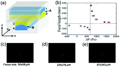 | ||
| Fig. 7 (a) A schematic drawing of the device. (b) Focal lengths of the cylindrical lenses focusing light along the x-axis (squares) and y-axis (crosses) as functions of the pressure differences. (c), (d) and (e) Demonstration of the laser mode. (c) Focusing in both directions; (d) Focusing in y direction; and (e) Focusing in x direction. Adapted from ref. 81, copyright 2005 Optical Society of America. | ||
Refractive index distribution of the liquid can also be modified by taking advantage of the fluid diffusion at the microscale level to form a refractive index gradient in the liquid medium, as shown in Fig. 8.82 A high-refractive index solution (nD = 1.455) was injected adjacent to a low refractive index solution (nD = 1.33). The diffusion between the fluids of the co-injected flows can form a refractive gradient, which can focus light in a way similar to the traditional gradient refractive index (GRIN) lens. The 2D refractive index profile and subsequently the focal length of the liquid GRIN (L-GRIN) lens can be tuned by changing the ratio of the flow rates of the injected solutions.
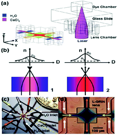 | ||
| Fig. 8 (a) The 2D L-GRIN lens structure and the diffusion of CaCl2 inside the L-GRIN lens chamber. (b) The side view of the refractive index distribution in the L-GRIN lens chamber. (c) The fluid injection setup of the 2D L-GRIN lens. (d) A microscopic image of the 2D diffusion pattern in the lens chamber. Reproduced from ref. 82. | ||
Pressure driven force is usually used to manipulate liquid flow, in which pressure is applied from outside the chip by either compressed air for fast response or height difference of the liquid for slow tuning. In these cases, reservoirs outside the chip are used for principle demonstration. However, for production operation, on-chip manipulation would be desired, such as electric actuation to modulate the chamber pressure (electroactive polymer,83,84 electromagnetic,85 or stimuli responsive hydrogel).86 However, for droplet formed lens, the effective manipulation would be electrowetting, which employs electrostatic forces to change the hydrophilicity of the solid–liquid or liquid–liquid interface. In this case, the surface tension changes the shape of the liquid surfaces87,88 and the sidewall electrode configuration,89,90 making the electrowetting lens a practical application.
Due to the many applications in biology, e.g. on-chip flow cytometry,91 in-plane adaptive lens were widely produced. Instead of membranes, fluids with different indices were used to form the geometric lens shape, while the pressure or flow difference was used to change the shape for adjusting the focal path. This is referred to as a liquid-core liquid-cladding (L2) lens, as shown in Fig. 9.92 Two streams of liquid with a lower refractive index (the cladding) sandwich a stream of liquid with a higher refractive index (the core). As the core stream enters the expansion chamber, it widens and becomes biconvex in shape for specific flow rates. This biconvex fluidic element focuses light. Manipulating the relative flow rates of the streams reconfigures the shape, and therefore adjusts the focal distance of the L2 lens. By offsetting the inlet and the outlet of the lens chamber to the chamber axis, Song et al.93 achieved a radius of curvature smaller than the limiting chamber radius, allowing for better focusing ability than the symmetric design.
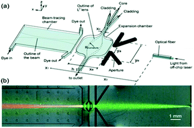 | ||
| Fig. 9 (a) Schematic of the liquid-core liquid-cladding (L2) lens. The channel for the formation of the L2 lens contains a square expansion chamber. The solid lines show the walls of the channel, and the dashed lines show the interfaces between the core and the cladding streams. (b) Bright-field image of the L2 lens in operation taken using a CCD camera to show the traces due to the fluorescence of the dye. Reproduced from ref. 92. | ||
Most of the optofluidic lenses are not tested for their imaging performance, but rather only for their dynamic focusing or beam shaping abilities. In optics, lens design and fabrication are complicated tasks because the imaging quality of a lens is strongly affected by the lens' surface, shape, curvature, size, material dispersion, as well as its variation with temperature and pressure.
Optofluidic focusing is a slow process due to the slow response of the fluid feeding/exchanging process. To increase the response time, frequency generated pressure control was introduced for high speed focusing, including 3D imaging generation. Campbell et al.94 designed adaptive lenses with millisecond response time that are based on transparent flexible elastomer membranes affixed to a plano-convex glass lens and a diaphragm between the membrane and the lens, as shown in Fig. 10. The membrane is optically flat. Instead of using a liquid, the application of vacuum to the interior of the mount pulls the membrane inward. Both the rise and fall transitions had very short onset time switches between flat segments and steep rise and fall segments occurring within 0.3 ms, suggesting that the lenses can be driven at frequencies up to 1600 Hz.
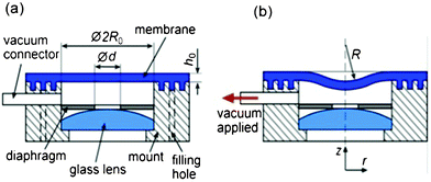 | ||
| Fig. 10 (a) Schematic of an adaptive compound camera lens with a flexible membrane, (b) the same camera lens with the membrane pulled inward when a vacuum is applied. Reproduced from ref. 94 with permission from the American Institute of Physics. | ||
Instead of moving a membrane, López et al.95 oscillated a drop of water trapped in a hole drilled in a Teflon plate to increase its focusing power. An audio speaker generated a sinusoidal pressure wave that drove the oscillations of the lens. In a period of oscillation the focal length evolved through its full range of values, and a synchronized high-speed camera captured sharp images at different focal planes. Speed of 10 ms was achieved. The combination of oscillating-focal-length lenses with high-speed cameras opens new possibilities for three-dimensional imaging devices.
6. Conclusions and outlook
As we have witnessed, the combination of optics with microfluidics has already changed our view about traditional optics by incorporating the properties of fluids to form novel optofluidic devices that combine the advantages of both to solve problems at the micro and nanoscale level. The customizability and compatibility of fluids with optical devices have enabled researchers to simplify previous complex processes, while also generating new optical devices that would be unfeasible without fluidic integration. Optofluidics has evolved into a diverse field: from optical property control, such as directional and focal point adjustment enabled by fluid manipulation to liquid photonics with more functionalities.It is certain that the complete integration of functionalities discussed here will be achieved and commercialized for on-chip source, manipulation, and detection for biochemical and biological applications. Furthermore, new research directions can also be envisioned.
As we have seen at the micrometer scale, current microfluidics exhibits no difficulty interfacing with the photonic design. However, as the photonic length scale reaches the nanometer region with the functional area down to tens of nanometers, mismatches between nanophotonics and nanofluidics become problematic, such as the issues of co-localization of bioreagents on nanometer sensors. The required alignment resolution is beyond current fabrication and processing capabilities. Therefore, novel approaches have to be formulated to align nanoresonators with nanofluidics.
The emergence of electronics and fluidics has been playing an important role in research and everyday life, such as electrowetting89 and liquid crystal display,96 assisted nanoparticle assembling,97 and nanopole DNA sequencing.98–100 Fully integrated opto-electro-fluidics at the micro and nanometer level will definitely enable more accurate and faster controls with added functionalities.
Current optofluidic sensors are designed to be employed for in vitro applications. Both photonics and microfluidics are designed for operation in a low background or interference environment. In in vitro operation, background interference can be eliminated by washing steps before signal readout. For in vivo configuration, no washing steps can be applied with biofouling being an inevitable problem. Serious breakthroughs have to be made in optofluidics before in vivo point of care diagnostics can become a reality.
Other prediction may also become reality within the next few years, like co-localization of single quantum dots in a nanoresonator for quantum analysis101,102 or optofluidics for energy generation and storage.103
Acknowledgements
The authors would like to acknowledge the support from the Defense Advanced Research Projects Agency (DARPA), the National Science Foundation (NSF), the NSF Center for Integrated Access Networks (CIAN), the Cymer Corporation, and the U.S. Army Research Office (ARO).References
- E. F. Borra, Astrophys. J., 1991, 373, 317–321 CrossRef.
- F. J. Duarte, L. W. Hillman, Dye Laser Principles, Academic, New York, 1990 Search PubMed.
- V. Studer, G. Hang, A. Pandolfi, M. Ortiz, W. F. Anderson and S. R. Quake, J. Appl. Phys., 2004, 95, 393–398 CrossRef CAS.
- M. A. Unger, H.-P. Chou, T. Thorsen, A. Scherer and S. R. Quake, Science, 2000, 288, 113–116 CrossRef CAS.
- T. Thorsen, S. J. Maerkl and S. R. Quake, Science, 2002, 298, 580–584 CrossRef CAS.
- T. M. Squires and S. R. Quake, Rev. Mod. Phys., 2005, 77, 977–1026 CrossRef CAS.
- J. W. Hong and S. R. Quake, Nat. Biotechnol., 2003, 21, 1179–1183 CrossRef CAS.
- D. B. Weibel, M. Kruithof, S. Potenta, S. K. Sia, A. Lee and G. M. Whitesides, Anal. Chem., 2005, 77, 4726–4733 CrossRef CAS.
- N. T. Nguyen and Z. G. Wu, J. Micromech. Microeng., 2005, 15, R1–R16 CrossRef.
- A. Gunther, M. Jhunjhunwala, M. Thalmann, M. A. Schmidt and K. F. Jensen, Langmuir, 2005, 21, 1547–1555 CrossRef.
- P. Garstecki, M. A. Fischbach and G. M. Whitesides, Appl. Phys. Lett., 2005, 86, 244108 CrossRef.
- ‘The origins the future of microfluidics‘ G. M. Whitesides, Nature, 2006, 442, 368–373 CrossRef CAS.
- F. Yeshaiahu, L. P. Lee, D. Psaltis, C. Yang, Optofluidics Fundamentals, Devices, and Application, McGraw-Hill, 2010 Search PubMed.
- D. Psaltis, S. R. Quake and C. Yang, Nature, 2006, 442, 381–386 CrossRef CAS.
- U. Levy and R. Shamai, Microfluid. Nanofluid., 2008, 4, 97–105 CrossRef.
- N.-T. Nguyen, Biomicrofluidics, 2010, 4, 031501 CrossRef.
- H. Schmidt and A. R. Hawkins, Nat. Photonics, 2011, 5, 598–604 CrossRef CAS.
- R. Hawkins, H. Schmidt, Handbook of Optofluidics, CRC Press, 2010 Search PubMed.
- Y. N. Xia and G. M. Whitesides, Annu. Rev. Mater. Sci., 1998, 28, 153–184 CrossRef CAS.
- M. A. Eddings, M. A. Johnson and B. K. Gale, J. Micromech. Microeng., 2008, 18, 067001 CrossRef.
- C. S. Effenhauser, G. J. M. Bruin, A. Paulus and M. Ehrat, Anal. Chem., 1997, 69, 3451–3457 CrossRef CAS.
- D. C. Duffy, J. C. M. Olivier, J. A. Schueller and G. M. Whitesides, Anal. Chem., 1998, 70, 4974–4984 CrossRef CAS.
- D. C. Duffy, O. J. A. Schueller, S. T. Brittain and G. M. Whitesides, J. Micromech. Microeng., 1999, 9, 211–217 CrossRef CAS.
- M. A. Eddings and B. K. Gale, J. Micromech. Microeng., 2006, 16, 2396–2402 CrossRef.
- K. Campbell, A. Groisman, U. Levy, L. Pang, S. Mookherjea, D. Psaltis and Y. Fainman, Appl. Phys. Lett., 2004, 85, 6119–6121 CrossRef CAS.
- M. I. Lapseley, S.-C. S. Lin and X. M. T. J. Huang, Appl. Phys. Lett., 2009, 95, 083507 CrossRef.
- W. Song and D. Psaltis, Lab Chip, 2011, 11, 2397–2402 RSC.
- A. Groisman, S. Zamek, K. Campbell, L. Pang, U. Levy and Y. Fainman, Opt. Express, 2008, 16, 13499–13508 CrossRef CAS.
- D. B. Wolfe, R. S. Conroy, P. Garstecki, B. T. Mayers, M. A. Fischbach, K. E. Paul, M. Prentiss and G. M. Whitesides, Proc. Natl. Acad. Sci. U. S. A., 2004, 101, 12434–12438 CrossRef CAS.
- J. Lim, J. P. Urbanski, T. Thorsen and S. Yang, Appl. Phys. Lett., 2011, 98, 044101 Search PubMed.
- U. Levy, K. Campbell and A. Groisman, Appl. Phys. Lett., 2006, 88, 111107 CrossRef.
- L. Pang, K. TeTz and Y. Fainman, Appl. Phys. Lett., 2007, 90, 111103 CrossRef.
- D. V. Vezenov, B. T. Mayers, R. S. Conroy, G. M. Whitesides, P. T. Snee, Y. Chan, D. G. Nocera and M. G. Bawendi, J. Am. Chem. Soc., 2005, 127, 8952–8953 CrossRef CAS.
- S. K. Y. Tang, Z. Li, A. R. Abate, J. J. Agresti, D. A. Weitz, D. Psaltis and G. M. Whitesides, Lab Chip, 2009, 9, 2767–2771 RSC.
- S. K. Y. Tang, R. Derda, Q. Quan, M. Lončar and G. M. Whitesides, Opt. Express, 2011, 19, 2204–2215 CrossRef CAS.
- Z. Y. Li, Z. Zhang, A. Scherer, D. Psaltis, Proceedings of the IEEE LEOS Summer Topics, Portland, 2007, 70–71 Search PubMed.
- J. D. Suter, Y. Sun, D. J. Howard, J. A. Viator and X. Fan, Opt. Express, 2008, 16, 10248–10253 CrossRef CAS.
- W. Lee, Y. Sun, H. Li, K. Reddy, M. Sumetsky and X. Fan, Appl. Phys. Lett., 2011, 99, 091102 CrossRef.
- S. I. Shopova, H. Zhou and X. Fan, Appl. Phys. Lett., 2007, 90, 221101 CrossRef.
- Y. Sun, S. I. Shopva, C. Wu, S. Arnold and X. Fan, Proc. Natl. Acad. Sci. U. S. A., 2010, 107, 16039–16042 CrossRef CAS.
- Z. Y. Li, Z. Zhang, T. Emery, A. Scherer and D. Psaltis, Opt. Express, 2006, 14, 6960–701 Search PubMed.
- Z. Y. Li, Z. Zhang, A. Scherer and D. Psaltis, Opt. Express, 2006, 14, 10494–10499 CrossRef CAS.
- W. Song, E. V. Andreas, Z. Li and D. Psaltis, Appl. Phys. Lett., 2009, 94, 161110 CrossRef.
- K. Kieu, L. Schneebeli, R. A. Norwood and N. Peyghambarian, Opt. Express, 2012, 20, 8148–8154 CrossRef CAS.
- P. Dumais, C. L. Callender, C. J. Ledderhof and J. P. Noad, Appl. Opt., 2006, 45, 9182–9190 CrossRef.
- P. Measor, L. Seballos, D. Yin, J. Z. Zhang, E. J. Lunt, A. R. Hawkins and H. Schmidt, Appl. Phys. Lett., 2007, 90, 211107 CrossRef.
- H. K. Hunt and A. M. Armani, Nanoscale, 2010, 2, 1544–1559 RSC.
- X. Fan and I. M. White, Nat. Photonics, 2011, 5, 591–597 CrossRef CAS.
- V. S.-Y. Lin, K. Motesharei, K.-P. S. Dancil, M. J. Sailor and M. R. Ghadiri, Science, 1997, 278, 840–843 CrossRef CAS.
- D. J. Bornhop, J. C. Latham, A. Kussrow, D. A. Markov, R. D. Jones and H. S. Sorensen, Science, 2007, 317, 1732–1736 CrossRef CAS.
- M. Armani, R. P. Kulkarni, S. E. Fraser, R. C. Flagan and K. J. Vahala, Science, 2007, 317, 783–787 CrossRef.
- W. Z. Song, A. Q. Liu, S. Swaminathan, C. S. Lim, P. H. Yap and T. C. Ay, Appl. Phys. Lett., 2007, 91, 223902 CrossRef.
- M. R. Lee and P. M. Fauchet, Opt. Express, 2007, 15, 4530–4535 CrossRef CAS.
- H. Raether, Surface Plasmons on Smooth and Rough Surfaces and on Gratings, Springer, Berlin, 1988, Search PubMed.
- C. Nylander, B. Liedberg and T. Lind, Sens. Actuators, 1982, 3, 79–88 CrossRef CAS.
- J. Homola, S. Yee and G. Gauglitz, Sens. Actuators, B, 1999, 54, 3–15 CrossRef.
- J. Homola, Surface Plasmon Resonance Based Sensors, Spring-Verlag, Berlin, 2006 Search PubMed.
- T. W. Ebbesen, H. J. Lezec, H. F. Ghaemi, T. Thio and P. A. Wolff, Nature, 1998, 391, 667–669 CrossRef CAS.
- A. G. Brolo, R. Gordon, B. Leathem and K. L. Kavanagh, Langmuir, 2004, 20, 4813–4815 CrossRef CAS.
- K. Tetz, L. Pang and Y. Fainman, Opt. Lett., 2006, 31, 1528–1530 CrossRef.
- A.-P. Blanchard-Dionne, L. Guyot, S. Patskovsky, R. Gordon and M. Meunier, Opt. Express, 2011, 19, 15041–15046 CrossRef.
- F. Eftekhari, R. Gordon, J. Ferreira, A. G. Brolo and D. Sinton, Appl. Phys. Lett., 2008, 92, 253103 CrossRef.
- M. E. Stewart, N. H. Mack, V. Malyarchuk, J. A. N. T. Soares, T.-W. Lee, S. K. Gray, R. G. Nuzzo and J. A. Rogers, Proc. Natl. Acad. Sci. U. S. A., 2006, 103, 17143–17148 CrossRef CAS.
- L. Pang, H. M. Chen, L. Wang, J. M. Beechem and Y. Fainman, Opt. Express, 2009, 17, 14700–14709 CrossRef CAS.
- J. N. Anker, W. P. Hall, O. Lyandres, N. C. Shah, J. Zhao and R. P. V. Duyne, Nat. Mater., 2008, 7, 442–453 CrossRef CAS.
- M. P. Jonsson, A. B. Dahlin, L. Feuz, S. Petronis and F. Hóök, Anal. Chem., 2005, 82, 2087–2094 CrossRef.
- N. Liu, L. M. Tang, M. Hentschel, H. Giessen and A. P. Alivisatos, Nat. Mater., 2011, 10, 631–636 CrossRef CAS.
- R. F. Ndangalia and S. V. Shabanov, J. Math. Phys., 2010, 51, 102901 CrossRef.
- Y. Zhang, T. Q. Jia, D. H. Feng and Z. Z. Xu, Appl. Phys. Lett., 2011, 98, 163110 CrossRef.
- Y. Lu, G. L. Liu, J. Kim, Y. X. Mejia and L. P. Lee, Nano Lett., 2005, 5, 119–124 CrossRef CAS.
- J. S. Shumaker-Parry, H. Rochholz and M. Kreiter, Adv. Mater., 2005, 17, 2131–2134 CrossRef CAS.
- H. M. Chen, L. Pang, A. King, G. M. Hwang, Y. Fainman, submitted.
- http://www.biacore.com .
- F. Eftekhari, C. Escobedo, J. Ferreira, X. Duan, E. M. Girotto, A. G. Brolo, R. Gordon and D. Sinton, Anal. Chem., 2009, 81, 4308–4311 CrossRef CAS.
- M. Huang, A. A. Yanik, T. Chang and T. H. Altug, Opt. Express, 2009, 17, 24224–24233 CrossRef CAS.
- D. Y. Zhang, V. Lien, Y. Berdichevsky, J. H. Choi and Y. H. Lo, Appl. Phys. Lett., 2003, 82, 3171 CrossRef CAS.
- A. Werber and H. Zappe, Appl. Opt., 2005, 44, 3238 CrossRef.
- N. Chronis, G. L. Liu, K. H. Jeong and L. P. Lee, Opt. Express, 2003, 11, 2370 CrossRef.
- K. H. Jeong, G. L. Liu, N. Chronis and L. P. Lee, Opt. Express, 2004, 12, 2494 CrossRef.
- D. Y. Zhang, N. Justis and Y. H. Lo, Appl. Phys. Lett., 2004, 84, 4194 CrossRef CAS.
- L. Pang, U. Levy, K. Campbell, A. Groisman and Y. Fainman, Opt. Express, 2005, 13, 9003–9013 CrossRef.
- H. Huang, X. Mao, S.-C. S. Lin, B. Kiraly, Y. Huang and T. J. Huang, Lab Chip, 2010, 10, 2387–2393 RSC.
- S. T. Choi, J. Y. Lee, J. O. Kwon, S. W. Lee and W. B. Kim, Proc. SPIE, 2008, 7208, 72080P Search PubMed.
- J. Y. Lee, S. T. Choi, S. W. Lee and W. B. Kim, Proc. SPIE, 2009, 7426, 742603 Search PubMed.
- S. W. Lee and S. S. Lee, Appl. Phys. Lett., 2007, 90, 121129 CrossRef.
- L. Dong, A. K. Agarwal, D. J. Beebe and H. R. Jiang, Nature, 2006, 442, 551–554 CrossRef CAS.
- X. F. Zeng and H. R. Jiang, Appl. Phys. Lett., 2008, 93, 151101 CrossRef.
- C. B. Gorman, H. A. Biebuyck and G. M. Whitesides, Langmuir, 1995, 11, 2242–2246 CrossRef CAS.
- B. Berge and J. Peseux, Eur. Phys. J. E., 2003, 159–163 Search PubMed.
- T. Krupenkin, S. Yang and P. Mach, Appl. Phys. Lett., 2003, 82, 316–318 CrossRef CAS.
- J. Godin, C.-H. Chen, S. H. Cho, W. Qiao, F. Tsai and Y.-H. Lo, J. Biophotonics, 2008, 1, 355–376 CrossRef CAS.
- S. K. Y. Tang, C. A. Stan and G. M. Whitesides, Lab Chip, 2008, 8, 395–401 RSC.
- C. Song, N.-T. Nguyen, S.-H. Tan and A. K. Asundi, J. Micromech. Microeng., 2009, 19, 085012 CrossRef.
- K. Campbell, Y. Fainman and A. Groisman, Appl. Phys. Lett., 2007, 91, 171111 CrossRef.
- C. A. López and A. H. Hirsa, Nature Photonics, 2008, 2, 595–596 CrossRef.
- M. Schadt, H. Seiberle and A. Schuster, Nature, 1996, 381, 212–215 CrossRef CAS.
- H. M. Chen, L. Pang, M. S. Gordon and Y. Fainman, Small, 2011, 7, 2750–2757 CrossRef CAS.
- S. Howorka, S. Cheley and H. Bayley, Nat. Biotechnol., 2001, 19, 636–639 CrossRef CAS.
- J. Clarke, H. Wu, L. Jayasinghe, A. Patel, S. Reid and H. Bayley, Nat. Nanotechnol., 2009, 4, 265–270 CrossRef CAS.
- M. Tsutsui, M. Taniguchi, K. Yokota and T. Kawai, Nat. Nanotechnol., 2010, 5, 286–290 CrossRef CAS.
- C. Ropp, R. Probst, Z. Cummins, R. Kumar, A. J. Berglund, S. R. Raghavan, E. Waks and B. Shapiro, Nano Lett., 2010, 10, 2525–2530 CrossRef CAS.
- R. Bose, D. Sridharan, H. Kim, G. S. Solomon and E. Waks, arXiv:1107.3751v1 Search PubMed.
- D. Erickson, D. Sinton and D. Psaltis, Nat. Photonics, 2011, 5, 583–590 CrossRef CAS.
Footnote |
| † Published as part of a themed issue on optofluidics |
| This journal is © The Royal Society of Chemistry 2012 |