Structural and morphological control of Mo doped titania films†
Chunxiang
Li
,
Zhongping
Yao
,
Guangmei
Wu
,
Zhaohua
Jiang
* and
Fangzhou
Jia
School of Chemical Engineering and Technology, Harbin Institute of Technology, Harbin 150001, China. E-mail: jiangzhaohua@hit.edu.cn; Fax: +86 451 86413709
First published on 22nd March 2011
Abstract
A facile and template-free layer-by-layer assembly-based method can be employed to synthesize structurally and morphologically controllable Mo-doped TiO2 films which demonstrate promising photoactivity.
Since the discovery of the photocatalytic splitting of water by Fujishima,1titania has been extensively used for applications, ranging from optoelectronics and photoelectrochemical to photocatalytic systems.2–4TiO2 has a number of advantageous properties, for instance being non-toxic, photo- and chemically stable, and relatively inexpensive. TiO2 is widely used for environmental remediation owing to the strong oxidative power of photogenerated holes, e.g., purification and treatment of polluted water and air. However, utilizing the photogenerated electrons for photocatalytic reactions, for example, splitting water into hydrogen, is impaired by its large band gap.5–7 Thus, it would be favorable if titania could be excited by the visible light. Numerous attempts have been carried out to reduce the band gap of TiO2 by anion- or cation-doping, further to enhance the photonic efficiencies. Therefore, various kinds of transition metals, including lower valent (+1, +2, +3), isovalent (+4) and higher valent (+5, +6) cations have been introduced into TiO2 for doping by different techniques.8–12
Conventional powder catalysts have the disadvantages: (1) agglomeration of nanoparticles is out of control, (2) separation of the final particle–fluid for catalyst recycling is difficult. Thus, many studies have been devoted to TiO2 thin films preparation by electrochemical, sol–gel and the layer-by-layer (LBL) technologies and great efforts have been conducted to enhance the photocatalytic activity of titania.13–15 It is known that the photoactivity of doped TiO2 is strongly dependent on the dopant concentration, the energy level of the dopant within the TiO2 lattice, the distribution of the dopant, the interfacial charge transfer as well as the geometries of titania.8 But the relationship between the sample fabrication history and morphology of sample has received considerably less attention, although different morphologies of the same material have different surface area ratios which affects the catalytic property greatly and some interesting progresses have been made in controlling the morphology and structure of carbon nanotubes.16–17 Recently, we fabricated and characterized Mo doped titania films after annealing at 500 °C,18 the films containing both anatase and rutile which were different from Mn and W-codoped titania films prepared by the LBL method.19Anatase titania has been reported to be more photocatalytically active than other forms of TiO2.20 Therefore, we execute further study in order to find out the effect of thermal treatment temperature on the morphology and structure of TiO2 films.
The pristine multilayer films build-up via the layer-by-layer method can be expressed as {[TALH/PEI]3/[Mo18/PEI]n/[TALH/PEI]3}2/TALH (abbr. pristine T-n), where n is the number of Mo18/PEI bilayers (Mo18: K6P2Mo18O62·14H2O; PEI: polyethylenimine and TALH: titanium(IV) bis(ammonium lactato) dihydroxide). Then, the pristine multilayer films were annealed at 200, 300, 400, 500 and 600 °C under ambient air for 2 hours, respectively, with a heating rate of 3 °C min−1. T-n or T-n/t is the abbreviation for product, where n is the number of Mo18/PEI bilayers in the pristine films and t is the temperature for annealing.
Morphological variations of T-2, T-4 and T-6 have been investigated. From Fig. 1, it can be seen that annealing temperature has a significant effect on the morphology of titania films. With the increase of temperature, all of the samples yielded regular patterns of morphology transition: cone/lamellar-stacked shapes to particles, and then nanorods. Addition of Mo can induce the morphology transition of the films at a lower annealed temperature. Take the images of T-2 for example, T-2/500 exhibits lamellar-stacked fragments with a size of 100–250 nm, while T-2/600 is composed of nanorods. T-4/500 shows aggregated TiO2 particles with the size range from 20 to 100 nm, while T-6/500 looks like many straight and smooth nanorods stacked together with the axes oriented in different directions. It is interesting to note that thermal treatment executed at high temperatures (≥500 °C) promotes the change in morphology of TiO2 films: nanorods and particles are fused into an indiscrete mass (Fig. S1, ESI†). However, with the addition of dopant, this morphology transition occurs at a lower temperature (ca. 700 °C for T-2, ca. 600 °C for T-6). These differences in morphology suggested that doping molybdenum could reduce the morphology transition temperature. Based on the energy dispersive X-ray spectroscopy (EDS) results (Fig. S2, ESI†), it can be found that the films are mainly composed of Si, Mo, Ti and O, while one part of the Si signal comes from the silane coupling agent and the other part is an artifact that comes from the substrate.
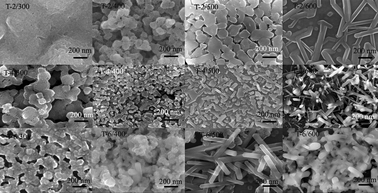 | ||
| Fig. 1 SEM images of T-2, T-4 and T-6 annealed at 300, 400, 500 and 600 °C, respectively. | ||
Fig. 2 shows typical TEM images of T-6/500 and T-6/600, respectively. The morphology of nanorods remains almost unchanged compared to regular nanorods. In this image (Fig. 2A), it is clear to see that fractal sheets that formed due to the decomposition of PEI and TALH in the process of thermal treatment self-organize into a well-ordered layer-by-layer structure and nanorod formed by aggregating some nanosized particles, which is different from the reported growth mechanism of nanowires.21 The HRTEM image shows the lattice fringes with an interplanar spacing of 0.047 nm corresponding to the (101) plane of anatase and 0.068 nm corresponding to the (110) plane of rutile for the titania crystal (Fig. 2B). However, the TEM image for T-6/600 changes intensely: nanorods disappear (Fig. 2a), the lattice fringes with an interplanar spacing of 0.117 nm corresponds to the (110) plane of rutile (Fig. 2b). The variation of lattice constant suggests that Mo atoms introduced by the LBL method enter into the TiO2 crystal lattice and substitute Ti due to similar ionic radius of Ti and Mo.18 Meanwhile, these results indicate that the sinter temperature can change not only the phase composition of the films but also the solubility of dopants that can alter the lattice constants.
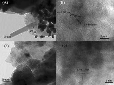 | ||
| Fig. 2 (A) and (a) Typical TEM images of T-6 annealed at 500 and 600 °C, respectively; (B) and (b) HRTEM image of the tip region in (A) and (a), respectively. | ||
In XPS measurements, the Mo concentration present in the films that is defined as the atomic percent of molybdenum with respect to titanium is estimated by the area ratio of Mo and Ti peaks. XPS measurements indicate that about 3.9%, 4.3% and 9.8% of atomic molybdenum concentrations are obtained by using ca. 7.25 × 10⁻⁴, 1.45 × 10⁻³ and 2.17 × 10⁻³ mg Mo18 for T-2, T-4 and T-6, respectively. The position of the main Ti 2p line at 464.1–464.5 eV proves the presence of Ti4+ in the films. The peak at 458.1 eV corresponds to the energy of the Ti–O bond in the Ti 2p spectrum of titania.22 Based on TEM analysis, with the increasing amount of molybdenum, the peak of Ti 2p shifts to higher binding energies of 458.7–458.3 eV gradually, attributed to the disordered titania crystal structure after molybdenum doping.23
A typical XPS survey scan of T-n/400 films is shown in Fig. 3. The main peaks in this figure are distinguished as C 1s, Ti 2p, O 1s, Mo 3d and Si 2p signals, corresponding to main peaks centered at 285.7 eV, 458.1 eV, 530.4 eV, 232.3 eV and 102.3 eV, respectively. The strong C peak can be assigned to sample surface contaminants. The O peak occurs mainly due to Ti–O in the TiO2 crystal lattice,19 and water absorbed on the surface of the films.24 The Mo peak is assigned to the dopant and fixed XPS peak positions of Mo3d in all samples shift to higher binding energies than that reported for MoO3.18 In addition, the peak value of the binding energy of the 2p orbitals of Si at 102.3 eV in Fig. 3 indicates that SiO2 was present.25 This result indicates that Si-based substrates formed SiO2 or Si-doped TiO2 was synthesized.
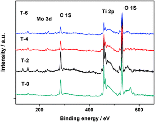 | ||
| Fig. 3 XPS survey scan of the films. | ||
An XRD measurement was carried out to determine their phase composition of the films. For normally grown titania films with a mixture of anatase and rutile, the mass fraction of rutile, WR, can be estimated using the followed formula, WR = 1/(1 + 0.8IA/IR), where IA and IR designate the X-ray integrated intensities of the (101) diffraction of anatase and the (110) diffraction of rutile, respectively.26 For T-n/500, the rutile content increases as the Mo6+ concentration changes from 3.9% to 9.8% (Table S1, ESI†) and the MoO3 phase appeared while the dopant content was >9.8%, while T-n/400 is the anatase phase and T-n/600 is the rutile phase, indicating that Mo6+ ions lead to a favorable formation of the rutile phase.18,27 Meanwhile, Mo-doped titania films (rutile phase) exhibit preferred orientation (Fig. S3, ESI†). Therefore, the morphology of Mo-doped titania films with high temperature thermal treatment becomes more and more ordered (shown in Fig. 1). In the present research, the rutile phase dominates (>50%) at 500 °C for the Mo doped TiO2, which is lower than that reported by Arroyo et al.28
The absorption spectra show the optical properties of doped and undoped films that annealed at 400 °C (Fig. S4, ESI†). In the case of undoped TiO2, the band structure is made up of the Ti 3d level and O 2p level that forms the conduction band and valence band, respectively, corresponding to the fundamental absorption edge at 380 nm. The occurrence of the doped-films' absorption edge shifts to the visible region is attributed to the electronic transition between the sub-band (closely related to the dopant and disordered lattice) and the band gap states of TiO2. The band gap energies of samples are ca. 3.1, 2.8, 2.6 and 2.2 eV for T-0, T-2, T-4 and T-6, respectively.10
It is reported that the anatase phase provides better photocatalytic activity than other forms of TiO2, such as rutile or brookite.20 Based on the above analysis, anchored to quartz slide titania films (40 × 25 mm) annealed at 400 °C are selected for photocatalytic activity studies. The specific surface area of the film was estimated by measuring N2 adsorption–desorption at 77 K using twenty glass substrates (24 × 5 × 0.3 mm) coated with the film on both sides, since the weight of a single layer film on a substrate was too small to be measured. The specific surface areas of the film were 103, 120, 156 and 184 m2 g−1 for T-0, T-2, T-4 and T-6, respectively. The photocatalytic activity of TiO2 films is evaluated by measuring H2 evolution from sacricial reagents (0.1 M SO32− and 0.05 M S2−). The photocatalytic experiments for all samples were carried out at the same time in batch type reactors equipped with a fixed extraposition lamp. A constant temperature was kept (T = 298 K) in each experiment. Prior to irradiation, a sacricial reagent (50 mL) was purged with nitrogen for 30 min. At given time intervals during the illumination, 5 mL portions of the resultant were taken out and further analyzed by gas chromatography (GC, HP 5890 II) equipped with TCD. The photocatalytic curves using an UV-rich source (P = 125 W, λ = 240–580 nm) are shown in Fig. 4. With the increase of the Mo/Ti molar ratio in the films, photocatalytic efficiency increases greatly and the catalytic efficiency of T-6 is higher than that of T-0, T-2 and T-4.
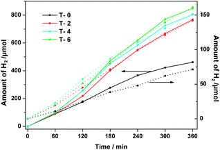 | ||
| Fig. 4 Photocatalytic hydrogen production under UV (solid line) and visible light (dot line) irradiations. Catalyst: TiO2 films (40 mm × 25 mm, ca. 2.11 × 10⁻⁴ g TiO2 loaded on the substrate). | ||
The photocatalytic H2 production under 500 W xenon lamp irradiations for T-0, T-2, T-4 and T-6 are shown in Fig. 4 also. It can be seen that the total amount of evolved H2 on T-6 is 162 μmol after 360 min, which is ca. 2.3 times higher than that on T-0 (71 μmol). UV-vis spectra show that introducing Mo6+ into TiO2 causes a shift of the absorption edge of TiO2 to the visible range, and the more the content of dopants, the larger is the red shift of the absorption edge. Therefore, the apparent photocatalytic activity of T-6 is slightly higher than that of T-2 and T-4. However, it is interesting to note that the photocatalytic activity difference for the undoped titania under UV and visible radiations is greater than that of doped films'. This may be because the dopant restricts itself in shifting the absorption edge to the visible region,29 which is in agreement with results of UV-vis spectra. More importantly, there is no distinct change in the physical properties of films after photoactivity measurements, indicating good stability of catalysts in the photocatalytic reaction.
In summary, Mo-doped TiO2 films with tunable morphology and controlled molybdenum concentration (up to 9.8%) have been successfully synthesized on the quartz substrates via the layer-by-layer assembly method. The morphology of the films changed from cone-stacked structures to particles, and then the structure changed to nanorods as the temperature for thermal treatment increased. It is conceivable that the molybdenum incorporated concentration significantly influences the temperature for both morphology and phase transition. Photocatalytic investigation reveals that the larger the dopant concentration, the lower the phase and structure transition temperature, and the higher the photocatalytic activity.
This work was financially supported by National 863 Project of China (Grant No. 2007AA03Z337).
Notes and references
- A. Fujishima and K. Honda, Nature, 1972, 238, 37 CAS.
- S. A. Tomás, S. Stolik, R. Palomino, R. Lozada, C. Persson, I. Pepe and A. Ferreira da Silva, J. Appl. Phys., 2005, 98, 73516 CrossRef.
- B. O'Regan and M. Grätzel, Nature, 1991, 353, 737 CrossRef CAS.
- T. L. Ma, K. Inoue, H. Noma, K. Yao and E. Abe, J. Photochem. Photobiol., A, 2002, 152, 207 CrossRef.
- M. Zhang, C. C. Chen, W. H. Ma and J. C. Zhao, Angew. Chem., Int. Ed., 2008, 47, 9730 CrossRef CAS.
- Y. G. Guo, J. S. Hu, H. P. Liang, L. J. Wan and C. L. Bai, Adv. Funct. Mater., 2005, 15, 196 CrossRef CAS.
- A. Yu, G. Q. M. Lu, J. Drennan and I. R. Gentle, Adv. Funct. Mater., 2007, 17, 2600 CrossRef CAS.
- W. Choi, A. Termin and M. R. Hoffmann, J. Phys. Chem., 1994, 98, 13669 CrossRef.
- B. Shahmoradi, I. A. Ibrahim, N. Sakamoto, S. Ananda, T. N. Guru Row, K. Soga, K. Byrappa, S. Parsons and Y. Shimizu, Environ. Technol., 2010, 31, 1213 CrossRef CAS.
- J. C. Colmenares, M. A. Aramendía, A. Marinas, J. M. Marinas and F. J. Urbano, Appl. Catal., A, 2006, 306, 120 CrossRef CAS.
- S. Roy, M. S. Hegde, N. Ravishankar and G. Madras, J. Phys. Chem. C, 2007, 111, 8153 CrossRef CAS.
- V. St'engl, S. Bakardjieva and N. Murafa, Mater. Chem. Phys., 2009, 114, 217 CrossRef CAS.
- L. Sun, J. Li, C. L. Wang, S. F. Li, H. B. Chen and C. J. Lin, Sol. Energy Mater. Sol. Cells, 2009, 93, 1875 CrossRef CAS.
- M. Răileanu, M. Crişan, N. Drăgan, D. Crişan, A. Galtayries, A. Brăileanu, A. Ianculescu, V. S. Teodorescu, I. Niţoi and M. Anastasescu, J. Sol-Gel Sci. Technol., 2009, 51, 315 CrossRef CAS.
- F. Caruso, X. Y. Shi, R. A. Caruso and A. Susha, Adv. Mater., 2001, 13, 740 CrossRef CAS.
- H. Liu, Y. Zhang, R. Y. Li, X. L. Sun, S. Désilets, H. A. Rachid, M. Jaidann and L. S. Lussier, Carbon, 2010, 48, 1498 CrossRef CAS.
- A. A. Kóos, M. Dowling, K. Jurkschat, A. Crossley and N. Grobert, Carbon, 2009, 47, 30 CrossRef CAS.
- C. X. Li, D. Zhang, Z. H. Jiang, Z. P. Yao and F. Z. Jia, New J. Chem., 2011, 35, 423 RSC.
- C. X. Li, Z. H. Jiang and Z. P. Yao, Dalton Trans., 2010, 39, 10692 RSC.
- M. A. Fox and M. T. Dulay, Chem. Rev., 1993, 93, 54.
- N. Wang, Y. Cai and R. Q. Zhang, Mater. Sci. Eng., R, 2008, 60, 1 CrossRef.
- D. Gonbeau, C. Guimon, G. Pfister-Guillouzo, A. Levasseur, G. Meunier and R. Dormoy, Surf. Sci., 1991, 254, 81 CrossRef CAS.
- H. Y. Ma, T. Dong, F. P. Wang, W. Zhang and B. B. Zhou, Electrochim. Acta, 2006, 51, 4965 CrossRef CAS.
- L. Q. Jing, B. F. Xin, F. L. Yuan, L. P. Xue, B. Q. Wang and H. G. Fu, J. Phys. Chem. B, 2006, 110, 17860 CrossRef CAS.
- Y. J. Zhang, X. F. Li, D. Chen, N. H. Ma, X. S. Hua and H. W. Wang, Scr. Mater., 2009, 60, 543 CrossRef CAS.
- J. M. Wu, H. Satoshi, K. Tsuru and A. Osaka, J. Am. Ceram. Soc., 2004, 87, 1635 CrossRef CAS.
- H. E. Chao, Y. U. Yun, H. U. Xingfang and A. Larbgot, J. Eur. Ceram. Soc., 2003, 23, 1457 CrossRef CAS.
- R. Arroyo, G. Cordoba, J. Padilla and V. H. Lara, Mater. Lett., 2002, 54, 397 CrossRef.
- L. G. Devi, S. G. Kumar, B. N. Murthy and N. Kottam, Catal. Commun., 2009, 10, 794 CrossRef CAS.
Footnote |
| † Electronic supplementary information (ESI) available: XRD, SEM and EDS results. See DOI: 10.1039/c1cy00024a |
| This journal is © The Royal Society of Chemistry 2011 |