Nanostructure formation via print diffusion etching through block copolymer templates
Ying
Liu
ab,
Jingcheng
Hao
ab and
Feng
Zhou
*ab
aState Key Laboratory of Solid Lubrication, Lanzhou Institute of Chemical Physics, Chinese Academy of Sciences, Lanzhou 730000, China. E-mail: zhouf@lzb.ac.cn
bGraduate School, Chinese Academy of Sciences, Beijing 100039, China
First published on 2nd February 2010
Abstract
The present work demonstrates nanoscale etching of silicon with standard aqueous fluoride etchants running through the hydrophilic domains of a vertically aligned copolymer template. The delivery of etchants was unprecedentedly achieved by an etchant-solution-saturated agarose gel stamp, a technique we call print diffusion etching. Three-dimensional nanoprotrusion features with controllable shapes and sizes (about 20 nm) were formed. To prove that the block copolymers serve to direct the silicon surface morphology by controlling the spatial location of the reaction as well as concentration of reagents, the same etching steps both on silicon and PS-b-PEO (polystyrene-block-polyethyleneoxide) templates were carried out for comparison. The mechanism of the nanoprotrusion formation was elucidated, and the morphology evolution vs. etching time studied.
Introduction
The fabrication of nanostructures with sub-30 nm feature size on silicon surfaces is urgently required for future nanoscopic functional components in silicon-based devices, but also a critical challenge.1 The most important representative top-down technique, photolithography, has seen decades of remarkable improvements, leading to the latest 45 nm feature size commercially available transistor technologies. Further decreases in size so as to increase chip densities are still expected. The sheer monetary and energetic costs of manufacturing such devices have reached an unprecedented magnitude, such as the use of X-ray lithography,2 micromachining,3,4 laser etching,5 electropolishing,6 dip-pen nanolithography (DPN)7 and reactive ion etching.8,9 Therefore, alternative strategies to produce patterned silicon architectures are under intense fundamental and industrial investigation as well.Polymer self-assembly has been considered as one approach to enable the uniform patterning of large areas of semiconductor interfaces.10–19 The technique depends on the spontaneous phase separation of block copolymers into nanoscale domains, which can be harnessed to produce periodic patterns.20–27 For instance, in 2003 IBM announced its intention to utilize self-assembled block copolymers to form quasi-hexagonal close-packed templates for the manufacture of floating silicon gates for flash memory.28 To some extent, polymer self-assembly is complementary to photolithography.
Recently, Qiao et al.28 used self-assembled PS-b-P4VP [polystyrene-block-poly-(4-vinyl pyridine)] for fabricating mesoscopic scale features on silicon-based materials and obtained etched nano-tips with diameters from 14 to 83 nm. The shape, size and morphology of the resulting etch pits can be readily modulated with variable etching conditions, such as time, fluoride concentration and silicon wafer orientation. However, the main drawback of a solution process is the consumption of a large amount to etchant solution, which poses a serious impact on environment unless additional post-treatment is adopted. In the present work, we have conducted selective etching on copolymer-template-coated silicon with a hydrophilic agarose gel stamp saturated with etchant solution. Slow diffusion of etchant through hydrophilic domains of copolymer template leads to local etching of silicon and the formation of nanostructures.
Agarose can dissolve in water when it is heated up to above 90 °C and turn to a semisolid elastic gel when the temperature falls to 35–40 °C. It has been used to make aqueous stamps for a few years.29–32 Presently, it is used as an etchant reservoir and provides etchant supply during stamping processes.33,34 In this paper the highly ordered nanostructured protrusions were formed on silicon wafers by etching hexagonally ordered phase-separated poly(styrene-block-ethylene oxide) (PS-b-PEO) films having a PEO vertical cylinder in a PS matrix, and this is the first time agarose gel has been introduced to carry out print diffusion etching on silicon.
Experiment
Materials
The diblock copolymer PS-b-PEO (Polymer Source) was used without further purification (molecular weight: Mn PS = 19 kDa, Mn PEO = 6.4 kDa, Mw/Mn = 1.05). Toluene, benzene and acetone were of analytical grade (SCRC, Sinapharm chemical reagent Co.). Silicon wafers (111, International Wafer Source, Inc.) were all cleaned and activated using oxygen plasma (100 W) for 30 min before use. Hydrofluoric acid (HF, 40%) and ammonium fluoride (NH4F) were purchased from SCRC. Surface topography of PS-b-PEO thin films on silicon wafer shards was imaged using a scanning force microscope (Nanoscope III, Digital Instruments Co.) in contact tapping mode.Templates
2 wt% PS-b-PEO in toluene was spin-coated onto silicon wafers (10 mm × 10 mm) at 3000 rpm for 20 s. Agarose (Type 1-B, Sigma) flat gel patterns were obtained by dispersing agarose powder in deionized water at 80 °C to get the flat gels. As-spun films were annealed in a small airtight vessel containing benzene and water vapor for 2 days at 5 °C to prepare the nanoporous structure.Etching
First, the flat agarose gels were soaked in HF/NH4F (v/v = 1/6; HF: 40% aq; NH4F![[hair space]](https://www.rsc.org/images/entities/char_200a.gif) :40% aq) solution for 2 min, and put them in contact with the PS-b-PEO templates for different period of time from 10 s to 30 min. The PS-b-PEO templates were completely washed away with acetone and deionized water. For comparison, gas-phase etching was also carried out. A small airtight vessel containing the silicon wafer and PS-b-PEO templates was well ventilated with hydrofluoric acid vapor for different time periods. Subsequently, the gas-etched templates were washed with acetone and deionized water.
:40% aq) solution for 2 min, and put them in contact with the PS-b-PEO templates for different period of time from 10 s to 30 min. The PS-b-PEO templates were completely washed away with acetone and deionized water. For comparison, gas-phase etching was also carried out. A small airtight vessel containing the silicon wafer and PS-b-PEO templates was well ventilated with hydrofluoric acid vapor for different time periods. Subsequently, the gas-etched templates were washed with acetone and deionized water.
Results and discussion
Templates
The amphiphilic block copolymer poly(styrene-block-ethylene oxide) (PS-b-PEO) was selected as the general polymer for template surface patterning because it self-assembles to well-aligned alternating hydrophilic PEO domains (green region in Scheme 1) and hydrophobic PS domains (red region in Scheme 1) after annealing in benzene and water vapor. The PEO blocks form densely packed, quasi-hexagonal vertical cylinders which are oriented normal to the surface of the film and span the entire film thickness, while PS resides form a matrix surrounding the PEO column as a result of the evaporation of toluene. Key to the conservation of topographic and morphological features of the polymer films in the course of the deposition and figuration is the temperature and humidity. Fig. 1(a) shows atomic force microscope (AFM) images of surface-reconstructed PS-b-PEO films on a native silicon substrate. The template consists of hexagonal cells in which the dark circular domains are PEO, which have a center-to-center distance of PEO of about 21.5 ± 2.2 nm and average diameter of 19.5 ± 1.5 nm (as determined in Fig. 1(b)). These results suggest that the cylindrical nanodomains of the PEO are normally oriented to the surface. Larger area (5 μm × 5 μm) and ordered arrangement self-assembled PS-b-PEO films are also prepared.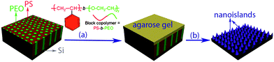 | ||
| Scheme 1 Schematic diagram of the synthesis of nanoprotrusions (b), on silicon by direct print diffusion etching with flat agarose gel saturated with HF/NH4F on self-assembled PS-b-PEO templates (a). | ||
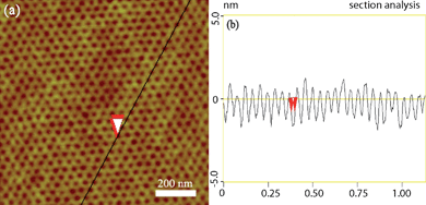 | ||
| Fig. 1 Phase-separated PS-b-PEO template. (a) AFM topography image of self-assembled PS-b-PEO block films, and (b) apparent topographic AFM profile taken along the line in (a). For AFM images the scan size is 1 μm × 1 μm, and the height scale is 10 nm. | ||
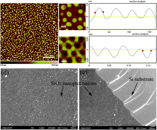 | ||
| Fig. 2 (a) AFM topography image of print-etched nanoprotrusions on silicon; (b) AFM topography image of print-etched nanoprotrusion on silicon, and the apparent topographic AFM profile taken along the line on the left; (c) AFM topography image of self-assembled PS-b-PEO blocks films, and apparent topographic AFM profile taken along the line on the left. The height scales are respectively 10 nm, 15 nm and 5 nm; (d) Top-view and (e) cross-sectional FESEM images of print-etched nanoprotrusions on silicon. | ||
Diffusion etching with flat agarose gels
Etching takes place exclusively beneath the vertical cylinders, in close proximity to the PEO blocks due to the highly flexible, loose, and hydrophilic PEO blocks, resulting in selective localization of HF solution within the PEO cylinder. The resulting high local concentration dot of silicon dioxide (SiO2) at the silicon surface is reminiscent of the well-studied PEO core, and is due to HF/NH4F etchant, typically used at high concentrations (v/v = 1/6; HF:40% aq; NH4F:40% aq). Silicon fluoride (SiF4) is the intermediate product of reaction between HF with SiO2, and it is produced when exposed Si reacts acutely with the water in the HF aqueous solution, subsequently producing metasilicic acid, and finally silicon dioxide as shown in the following equation. Therefore, SiO2 stays at the center as the nanoprotusion, replacing the PEO column after cleaning the templates, because it is trapped under the barrier of the agarose gel pattern above. As such, our outcome is converse to the nano-tip etching in HF solution.28
The reaction between silicon and silicon dioxide:
| SiO2 + 4HF → SiF4 + 2H2O |
The reaction between silicon and hydrofluoric acid:
| Si + 4HF → SiF4 + 2H2↑ |
The reaction between silicon fluoride and water:
| SiF4 + 3H2O → H2SiO3 + 4 HF↑ |
| H2SiO3 → H2O + SiO2 |
Top-view AFM images [Figs. 2(a) and 2(b)] show the formation of pseudo-hexagonal etched dots with a diameter of 20 nm, identical to that of the parent template. As shown in the plane and tridimensional view atomic force microscopy images of etched PS-b-PEO templates [Fig. 2(a)], the etched bumped dot developed underneath the PEO column center of the block copolymer film. After removing the polymer film by cleaning the wafer shard with acetone and deionized water, the well-defined etched dot arrays are revealed. Comparison of surface topography between the self-assembled templates [Fig. 2(c)] and print-etched dot on silicon [Fig. 2(b)] is shown in Fig. 2, where we can see that they match very well.
X-ray photoelectron spectroscopy (XPS) was performed on the as-prepared self-assembled PS-b-PEO templates (Fig. 3, in red) and after cleaning the print-etched templates (Fig. 3, in black) to further verify the surface composition. As shown in the corresponding full XPS spectrum [Fig. 3(a)], the wide-scan spectra of both PS-b-PEO templates and surface after cleaning template are dominated by signals attributable to silicon, oxygen and carbon. Remarkable quantitative variance occurred for the C 1s as the multielement spectrum of XPS shown in Fig. 3(b). The molar ratio of C/O is 0.49 (the black one) after cleaning polymer template, while the value is 11.6 (the red one) in template. It is also worth noting that the vibration-induced peak of C1s in PS appeared at about 292.0 eV, and the peak disappeared after rinsing the template, which indicates that the nanostructure of the print-etched surface didn't result from polymer contamination. We also calculated the ratio of Si to O before and after the formation of nanoprotrusions from XPS data. The ratio of Si to O increased from 52:48 to 31:69 indicating a chemical change in the etching process which formed a new material containing more oxygen. The X-ray diffraction (XRD) results indicate that the new composition was amorphous SiO2, shown in Fig. 3(c).
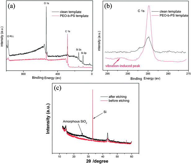 | ||
| Fig. 3 (a, b) XPS spectra of the self-assembled PS-b-PEO templates (in red) and print-etched nanoprotrusion on silicon after cleaning the templates (in black). (c) XRD patterns of the samples before and after print-etching. | ||
The existence of nanoprotrusions was also proved by water contact angle measurements after print diffusion etching, taking off the flat agarose pattern and cleaning the self-assembled PS-b-PEO templates completely. As predicted, the water contact angle of the silicon surface changed from 30.5° [Fig. 4(a)] to a maximum value of 95.2° after print diffusion etching [Fig. 4(b)]. The presence of nanoprotrusions on the silicon surface increases the roughness of the silicon surface, and the water contact angle increased by 65° as a result.
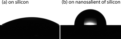 | ||
| Fig. 4 Water contact angle of water on silicon surface (a) 30.5° to a maximum value of 95.2° after modification by print diffusion etching (b). | ||
Etching time can affect the surface topography. The variations of height, shape and density of the dot arrays with the etch time for 10 s, 1 min, 10 min, 30 min are shown in Fig. 5. Etching time appears to play hardly any role in the shape and dimension of etching dots, which should be governed by the size of the PEO domains. This, on the other hand, verifies the nanoconfinement effect of the polymer template on etchant diffusion that dominates the PEO cylindrical domains. Normally, the height and density of the bulging outward are affected a lot at the initial stage from 10 s to 1 min [Figs. 5(a) and 5(b)], afterwards, they change little when extending the etch time to 10 min [Fig. 5(c)]. It is also seen from Fig. 5(d) that connection between two adjacent nanoprotrusions occurred after too long an etchant diffusion time, 30 min, indicating the reaction expanded laterally due to lateral diffusion of etchant.
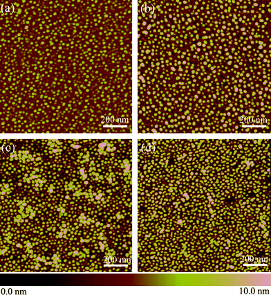 | ||
| Fig. 5 Planar AFM images of the print-etched dots on silicon after cleaning the self-assembled PS-b-PEO templates, at different etch times. (a) 10 s, (b) 1 min, (c) 10 min and (d) 30 min. For all AFM images the scan size is 1 μm × 1 μm and the height scale is 10 nm. | ||
:40% aq; NH4F:40% aq) were pressed onto silicon directly for different times, such as 2, 5 and 30 min, and then cleaned with deionized water to remove the remaining HF/NH4F solution after taking off the agarose pattern. Surface topography changes a lot with the print-etching time as shown in the AFM images in Fig. 6.
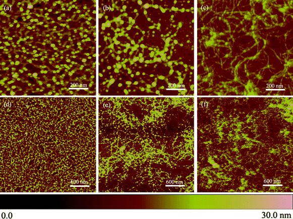 | ||
| Fig. 6 AFM images of the print-etched nanoprotrusions directly on silicon at different etch times. (a, d) 2 min; (b, e) 5 min; (c, f) 30 min. For all AFM images the scan size is 1 μm × 1 μm in (a–c), and 3 μm × 3 μm in (b–f); the height scale is 30 nm. | ||
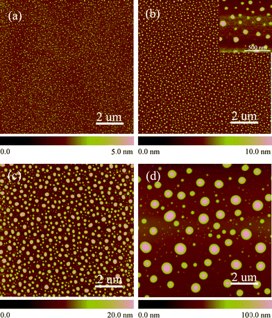
Firstly, surface morphology evolved dramatically with the etching time. Some dots were generated but intrinsically interconnected to form porous surfaces for a short time [2 min in Figs. 6(a) and 6(d)]. The free diffusion of the dots in arbitrary directions became restricted as the etch time was prolonged [5 min, as shown in Figs. 6(b) and 6(e)], consequently, all dots vanished to form intertwined lines when the etching time increased to 30 min [shown in Figs. 6(c) and 6(f)]. Secondly, the depth of print-etch is much higher than that with the template due to the fact that abundant etchant was in contact with surface. The most distinguishing characteristic in the presence of polymer template is that the free diffusion of etchant and etching reaction are liable to occur in the lateral direction, resulting in a featureless morphology. It is thus clear that the existence of self-assembled PS-b-PEO templates governs the diffusion of etchant into PEO domains only, leading to separated nanoprotrusions.
Gas-etching with HF vapor on self-assembled templates and silicon
To further demonstrate diffusion of etchant through PEO domains in the polymer template, we performed gas-diffusion etching using HF vapor. Qiao et al.28 etched silicon with HF in HF/NH4F solution. PS-b-PEO coated silicon was put into a small airtight vessel and flushed with saturated hydrofluoric acid vapor for different time periods and cleaned with acetone and deionized water. The variations of surface morphology with etch time are shown in Fig. 7. The nanoprotrusions get higher and higher with the gas-etching time as shown in Fig. 7. The size is about 20 nm at the initial stages [Figs. 7(a)–(b)], the same size as the PEO vertical cylinders in templates, when the etch time reached 30 min [Fig. 7(d)], the size expanded to 40 nm. This implies that the existence of self-assembled templates can control the dimensions of the etching pits, however, if the etch time were to be increased further, the nanoconfinement effect will be lost due to overwhelming etchant. The flat agarose gel provides perfect reservoir for mild supply of etchant in nanoconfined space, displaying an outstanding superiority in comparison with direct gas-etching. However, etching with HF vapor on blank silicon surfaces resulted in a drastically different morphology (AFM images are shown in Fig. 8). The etching pits are generated although uniformly on silicon, but with very low density (see the inset in Fig. 8b). The size of each etching pits grew up very rapidly to several hundreds nanometres and reached to over a hundred nanometres in height after 60 min treatment time. This is in clear contrast that in Fig. 7, where polymer template guided diffusion-etching was evident.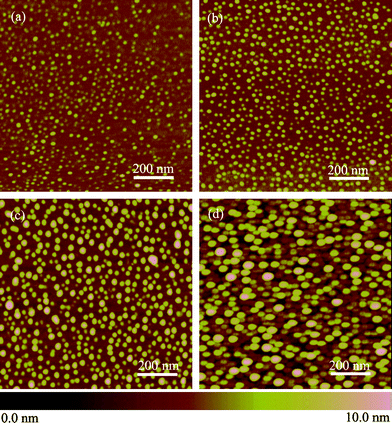 | ||
| Fig. 7 Planar AFM images of the gas-etched dots on silicon, after cleaning the self-assembled PS-b-PEO templates, at different etch times. (a) 10 s, (b) 1 min, (c) 10 min and (d) 30 min. For all AFM images the scan size is 1 μm × 1 μm and the height scale is 10 nm. | ||
 | ||
| Fig. 8 Planar AFM images of the gas-etched dots on silicon at different etch times. (a) 30 s, (b) 1 min, (c) 10 min and (d) 60 min. For all AFM images the scan size is 10 μm × 10 μm; The height scale is 10 nm and the height scale is marked in all images. | ||
Conclusion
In this article, we have reported a novel approach to carry out copolymer nanolithography using a diffusion-etching process with hydrophilic agarose gel stamps as the etchant reservoir. The delivery of etchant was unprecedentedly achieved by diffusion of standard aqueous fluoride etchant running through the hydrophilic domains of a vertically aligned copolymer template. Nanostructural dot features with controllable shapes and sizes (about 20 nm) were formed on the silicon surface due to the nanoconfinement effect. To prove that the block copolymers serve to direct the silicon surface chemistry by controlling the spatial location of the reaction as well as concentration of reagents, the same etching steps on both silicon and PS-b-PEO templates were carried out for comparison. Print diffusion etching and gas-etching on both polymer template-coated silicon and blank silicon were also carried out as controls, further verifying the important role of the polymer template in governing etchant diffusion. The idea of contact diffusion printing is just at its starting point. The application of well-ordered PS-b-PEO templates and the hydrophilic PEO cylinder as a run-through channel will be useful in future nanofabrication.Acknowledgements
The authors gratefully acknowledge the “Hundred Talents Program” of CAS, the NSFC (50721062) and the “973” Project (2007CB607601).References
- J. V. Barth, G. Costantini and K. Kern, Nature, 2005, 437, 671 CrossRef CAS.
- X. M. Yang, R. D. Peters, T. K. Kim and P. F. Nealey, Langmuir, 2001, 17, 228 CrossRef CAS.
- N. R. Tas, J. W. Berenschot, P. Mela, H. V. Jansen, M. Elwenspoek and A. van den Berg, Nano Lett., 2002, 2, 1031 CrossRef CAS.
- P. Allongue, P. Jiang, V. Kirchner, A. L. Trimmer and R. Schuster, J. Phys. Chem. B, 2004, 108, 14434 CrossRef CAS.
- S. H. Wong, M. Thiel, P. Brodersen, D. Fenske, G. A. Ozin, M. Wegener and G. von Freymann, Chem. Mater., 2007, 19, 4213 CrossRef CAS.
- S. Singh, W. R. T. Barden and P. Kruse, ACS Nano, 2008, 2, 2453 CrossRef CAS.
- M. Su, X. G. Liu, S. Y. Li, V. P. Dravid and C. A. Mirkin, J. Am. Chem. Soc., 2002, 124, 1560 CrossRef CAS.
- M. Park, C. Harrison, P. M. Chaikin, R. A. Register and D. H. Adamson, Science, 1997, 276, 1401 CrossRef CAS.
- R. G. H. Lammertink, M. A. Hempenius, J. E. van den Enk, V. Z. H. Chan, E. L. Thomas and G. J. Vancso, Adv. Mater., 2000, 12, 98 CrossRef CAS.
- (a) J. P. Spatz, S. Mössmer, C. Hartmann, M. Moller, T. Herzog, M. Krieger, H. G. Boyen, P. Ziemann and B. Kabius, Langmuir, 2000, 16, 407 CrossRef CAS; (b) J. P. Spatz, T. Herzog, S. Mössmer, P. Ziemann and M. Moller, Adv. Mater., 1999, 11, 149 CrossRef CAS; (c) Y. H. La, E. W. Edwards, S. M. Park and P. F. Nealey, Nano Lett., 2005, 5, 1379 CrossRef CAS; (d) J. Y. Cheng, C. A. Ross, V. Z-H. Chan, E. L. Thomas, R. G. H. Lammertink and G. J. Vancso, Adv. Mater., 2001, 13, 1174 CrossRef CAS.
- V. Luchnikov, A. Kondyurin, P. Formanek, H. Lichte and M. Stamm, Nano Lett., 2007, 7, 3628 CrossRef CAS.
- Y. Wang, J. Q. Liu, S. Christiansen, D. H. Kim, U. Gösele and M. Steinhart, Nano Lett., 2008, 8, 3993 CrossRef CAS.
- Y. S. Jung, W. Jung, H. L. Tuller and C. A. Ross, Nano Lett., 2008, 8, 3776 CrossRef CAS.
- S. H. Kim, F. Nederberg, L. Zhang, C. G. Wade, R. M. Waymouth and J. L. Hedrick, Nano Lett., 2008, 8, 294 CrossRef CAS.
- M. P. Stoykovich, H. Kang, K. Ch Daoulas, G. L. Liu, C. C. Liu, J. J. de Pablo, M. Müller and P. F. Nealey, ACS Nano, 2007, 1, 168 CrossRef CAS.
- (a) K. Shin, K. Amanda Leach, J. T. Goldbach, D. H. Kim, J. Y. Jho, M. Tuominen, C. J. Hawker and T. P. Russell, Nano Lett., 2002, 2, 933 CrossRef CAS; (b) S. Krishnamoorthy, R. Pugin, J. Brugger, H. Heinzelmann, A. C. Hoogerwerf and C. Hinderling, Langmuir, 2006, 22, 3450 CrossRef CAS.
- (a) M. R. Bockstaller, R. A. Mickiewicz and E. L. Thomas, Adv. Mater., 2005, 17, 1331 CrossRef CAS; (b) S. Park, J. Y. Wang, B. Kim, W. Chen and T. P. Russell, Macromolecules, 2007, 40, 9059 CrossRef CAS; (c) S. Ludwigs, K. Schmidt and G. Krausch, Macromolecules, 2005, 38, 2376 CrossRef CAS.
- S. Ludwigs, A. Böker, A. Voronov, N. Rehse, R. Magerle and G. Krausch, Nat. Mater., 2003, 2, 744 CrossRef CAS.
- (a) S. Ludwigs, G. Krausch and R. Magerle, Macromolecules, 2005, 38, 1859 CrossRef CAS; (b) D. Yin and S. Horiuchi, Chem. Mater., 2005, 17, 463 CrossRef CAS; (c) T. Thurn-Albrecht, J. Schotter, G. A. Kästle, N. Emley, T. Shibauchi, L. Krusin-Elbaum, K. Guarini, C. T. Black, M. T. Tuominen and T. P. Russell, Science, 2000, 290, 2126 CrossRef CAS; (d) D. Zschech, D. H. Kim, A. P. Milenin, R. Scholz, R. Hillebrand, C. J. Hawker, T. P. Russell, M. Steinhart and U. Go1sele, Nano Lett., 2007, 7, 1516 CrossRef CAS.
- S. Park, J. Y. Wang, B. Kim, J. Xu, P. Thomas and T. P. Russell, ACS Nano, 2008, 2, 766 CrossRef CAS.
- (a) M. P. Stoykovich, M. Muller, S. O. Kim, H. H. Solak, E. W. Edwards, J. J. de Pablo and P. F. Nealey, Science, 2005, 308, 1442 CrossRef CAS; (b) I. W. Hamley, Angew. Chem., Int. Ed., 2003, 42, 1692 CrossRef CAS; (c) M. Aizawa and J. M. Buriak, J. Am. Chem. Soc., 2005, 127, 8932 CrossRef CAS.
- M. L. van Poll, F. Zhou, M. Ramstedt, L. Hu and W. T. S. Huck, Angew. Chem., Int. Ed., 2007, 46, 6634 CrossRef CAS.
- D. A. Olson, L. Chen and M. A. Hillmyer, Chem. Mater., 2008, 20, 869 CrossRef CAS.
- Y. S. Jung and C. A. Ross, Nano Lett., 2007, 7, 2046 CrossRef CAS.
- J. Rzayev and M. A. Hillmyer, J. Am. Chem. Soc., 2005, 127, 13373 CrossRef CAS.
- J. Y. Cheng, F. Zhang, V. P. Chuang, A. M. Mayes and C. A. Ross, Nano Lett., 2006, 6, 2099 CrossRef CAS.
- (a) S. H. Kim, M. J. Misner and T. P. Russell, Adv. Mater., 2004, 16, 2119 CrossRef CAS; (b) M. Lazzari and M. Arturo López-Quintela, Adv. Mater., 2003, 15, 1583 CrossRef CAS; (c) J. Bang, S. H. Kim, E. D. kenmuller, M. J. Misner, T. P. Russell and C. J. Hawker, J. Am. Chem. Soc., 2006, 128, 7622 CrossRef CAS; (d) Z. Q. Lin, D. H. Kim, X. D. Wu, L. Boosahda, D. Stone, L. LaRose and T. P. Russell, Adv. Mater., 2002, 14, 1373 CrossRef CAS; (e) S. H. Kim, M. J. Misner, T. Xu, M. Kimura and T. P. Russell, Adv. Mater., 2004, 16, 226 CrossRef CAS.
- Y. H. Qiao, D. Wang and J. M. Buriak, Nano Lett., 2007, 7, 464 CrossRef CAS.
- G. Mahmud, K. J. M. Bishop, Y. Chegel, S. K. Smoukov and B. A. Grzybowski, J. Am. Chem. Soc., 2008, 130, 2146 CrossRef CAS.
- C. J. Campbell, R. Klajn, M. Fialkowski and B. A. Grzybowski, Langmuir, 2005, 21, 418 CrossRef CAS.
- S. K. Smoukov, A. Bitner, C. J. Campbell, K. Kandere-Grzybowska and B. A. Grzybowski, J. Am. Chem. Soc., 2005, 127, 17803 CrossRef CAS.
- (a) M. Mayer, J. Yang, I. Gitlin, D. H. Gracias and G. M. Whitesides, Proteomics, 2004, 4, 2366 CrossRef CAS; (b) D. B. Weibel, A. Lee, M. Mayer, S. F. Brady, D. Bruzewicz, J. Yang, W. R. DiLuzio, J. Clardy and G. M. Whitesides, Langmuir, 2005, 21, 6436 CrossRef CAS.
- S. K. Smoukov, K. J. M. Bishop, R. Klajn, C. J. Campbell and B. A. Grzybowski, Adv. Mater., 2005, 17, 1361 CrossRef CAS.
- S. K. Smoukov and B. A. Grzybowski, Chem. Mater., 2006, 18, 4722 CrossRef CAS.
| This journal is © The Royal Society of Chemistry 2010 |