
Single-molecule non-volatile memories: an overview and future perspectives
Wei
Si†
a,
Junhao
Li†
b,
Guangwu
Li
*a,
Chuancheng
Jia
 *a and
Xuefeng
Guo
*ab
*a and
Xuefeng
Guo
*ab
aCenter of Single-Molecule Sciences, Institute of Modern Optics, Frontiers Science Center for New Organic Matter, College of Electronic Information and Optical Engineering, Nankai University, 38 Tongyan Road, Jinnan District, Tianjin 300350, P. R. China. E-mail: guoxf@pku.edu.cn; jiacc@nankai.edu.cn; ligw@nankai.edu.cn
bBeijing National Laboratory for Molecular Sciences, National Biomedical Imaging Center, College of Chemistry and Molecular Engineering, Peking University, Beijing 100871, P. R. China
First published on 30th November 2023
Abstract
Single-molecule non-volatile memories can be designed as high-density memories and memristors. The latter, enabling real-time data processing by performing computations directly within the memory unit, holds the potential to surpass the limitations predicted by the Von Neumann architecture. This article provides an overview of the research progress on non-volatile memories associated with functional centers of single molecules. Single-molecule devices with bistable or even multistable switching characteristics have been used to achieve storage and memory resistance functions. This review aims to summarize strategies for achieving non-volatile resistance switching using single-molecule devices, including the design of functional molecules and device construction. It uncovers the physical and chemical mechanisms by which single-molecule non-volatile memories realize multistable conductance states, such as conformational transformations, tautomerisms, intramolecular motions, spin changes, and charge changes. Furthermore, it discusses the potential developments and challenges of single-molecule non-volatile memories, including the diversity in device construction, the challenges of device integration, and the possibility of achieving the high performance, while proposing potential solutions. The objective of this review is to provide readers with fresh research insights and avenues for further exploration, thereby introducing new perspectives in the field of single-molecule non-volatile memories.
 Wei Si | Wei Si is currently a PhD candidate in the Center of Single-Molecule Science, Institute of Modern Optics, College of Electronic Information and Optical Engineering, Nankai University, with Prof. Xuefeng Guo. His research is focused on single-molecule electronics. |
 Junhao Li | Junhao Li received his BS degree in 2022 from the College of Chemistry and Molecular Engineering, Peking University. He is currently a PhD candidate at the College of Chemistry and Molecular Engineering, Peking University, under the guidance of Prof. Xuefeng Guo. His current research is focused on the integration of single-molecule devices. |
 Guangwu Li | Prof. Guangwu Li received his BS degree in 2010 from Beijing Normal University (BNU), and then he obtained PhD degree in 2015 also at BNU under supervision of Prof. Zhishan Bo. Then he moved to National University of Singapore (NUS) working as research fellow under the supervision of Prof. Jishan Wu. He is now working as an associate professor in College of Electronic Information and Optical Engineering, Nankai University. His major interests lie mainly in developing novel π-conjugated systems, particularly with magnetic properties. |
 Chuancheng Jia | Prof. Chuancheng Jia received his PhD degree in 2014 from the College of Chemistry and Molecular Engineering, Peking University, under the guidance of Prof. Xuefeng Guo. From 2014 to 2020, he was a postdoc at the Institute of Chemistry, Chinese Academy of Sciences and University of California, Los Angeles. He joined the faculty as a professor at Nankai University in 2020. His research is focused on single-molecule electronics and dynamics. |
 Xuefeng Guo | Prof. Xuefeng Guo received his BS degree in 1998 from Beijing Normal University and his PhD degree in 2004 from the Institute of Chemistry, Chinese Academy of Sciences, Beijing. From 2004 to 2007, he was a postdoc at the Columbia University Nanocenter. He joined the faculty as a professor under “Peking 100-Talent” Program at Peking University in 2008. His current research is focused on functional nanometer/molecular devices. |
1. Introduction
In the contemporary digital age, data memories have emerged as a linchpin of technological advancement. Memories, a broad term that refers to repositories for data conservation, include among their ranks the subset of non-volatile memories.1–7 These are characterized by their ability to retain information even in the absence of external energy input. Resistive memory stands out as a novel technique within the non-volatile memory category, operating on the principle of resistance alterations within the material.8,9 Specific electronic switches are typically employed to control and read these resistance changes. In many applications, non-volatile memory offers unique advantages. For instance, the memristor, a specific form of non-volatile memories, can break away from the von Neumann architecture, achieving unified memory and computation.10–12 However, as technologies like big data platforms, the internet of things, and artificial intelligence rapidly evolve, the demands for memory density, speed, and endurance have concurrently risen.13,14 While traditional memories have served us commendably over past decades, their inherent physical dimensions and speed constraints are becoming inadequate for future requirements.15Single-molecule devices, a facet of nanotechnology, renowned for their minute size and rich functionality, have piqued the interest of researchers globally.16–18 Contemporary research studies on single-molecule devices primarily concentrate on two approaches: one is to regulate the basic physical properties of single molecules, and the other is to realize the functionalization of single-molecule devices.19–22 This encompasses considerations such as electrode material selection, interface linkages, molecular functional center design, and the introduction of external fields for regulating molecular properties.23–25 Owing to the diverse and tunable designs of both devices and molecules, single-molecule devices offer innovative research avenues in electronics, optoelectronics, and spintronics, achieving noteworthy accomplishments.26–28 Recent findings in single-molecule electronics demonstrate the feasibility of stable bistable conductive states at the single-molecule scale. This suggests that a molecule can alternate between two distinct conductive states and maintain these states under working conditions. Such a characteristic lays the foundation for non-volatile memories, as binary data can be represented via these two stable molecular states. For instance, source–drain electrodes, while providing working voltages, may also alter a molecule's redox state or influence its conformation, thereby affecting its conductivity.29–31 To devise and fabricate efficient single-molecule non-volatile memories, the mechanism of molecular bistability must be thoroughly investigated. This entails understanding molecular responses under varying conditions and governing molecular states through external stimuli such as a light field, an electric field or a magnetic field.32,33 Furthermore, practical implementation necessitates the integration of these molecules with microelectronic devices, ensuring the compatibility between single-molecule devices and conventional devices during fabrication, and leveraging existing semiconductor manufacturing processes for mass production. Research in single-molecule non-volatile memories not only offers profound insights into the particular properties of a single molecule, but also charts a novel trajectory for future data memory and memristor computing. With the rapid progression of single-molecule science and semiconductor fabrication techniques, single-molecule non-volatile memories are poised for extensive applications in the future.
This review encapsulates recent research reports in the domain of single-molecule devices, aiming to furnish readers with a comprehensive overview of single-molecule non-volatile memories. The initial section elucidates fabrication methodologies of single-molecule non-volatile memories. The second part summarizes the basic principles and evolutionary trajectories of single-molecule non-volatile memories. The concluding remarks spotlight the existing challenges and impediments in the realm of single-molecule non-volatile memories, expressing our aspiration that this exposition might kindle heightened interest among researchers in this sector, laying a robust foundation for future investigations and memory applications.
2. Design and construction of single-molecule non-volatile memories
In this chapter, we delve into the structural basis of various devices in the realm of single-molecule non-volatile memories. Our focus is to methodically elucidate an array of device architectures, each contributing distinctly to the development of single-molecule technologies. The discourse covers a wide range of state-of-the-art approaches, from single-molecule junctions to vertical molecular tunneling devices, with each typified by unique material properties and sophisticated fabrication methodologies. This chapter acts as a pivotal link that seamlessly transits from the foundational principles previously discussed to a detailed exploration of diverse device structures. It aims to furnish a comprehensive contextual understanding, which is critical for comprehending the ongoing technological innovations and challenges in the field of single-molecule non-volatile memories.2.1 Preparation of single-molecule devices
The development of a methodology for preparation of single-molecule devices opens up new possibilities for exploring the physical properties of single molecules and constructing prototype devices including molecular memory. From a structural standpoint, single-molecule devices primarily consist of three components: electrodes, functional molecules, and contact interfaces, which correspond to different aspects of the preparation process: material engineering, molecular engineering, and interface engineering, respectively. Molecular engineering plays a central role in device construction, as it involves designing the molecular structure to achieve specific functions. Material engineering includes selection and process of electrodes at the nanometer scale. Interface engineering studies the connection and coupling between molecule and electrodes, which determines the achievement of functional molecules. At present, the preparation of single-molecule devices has been a mature and reliable process. This part we mainly introduce the preparation process of the device and comparison of the different methods. Accordingly, the design of molecules with the function of the memory is described in the next chapter. Divided by electrode material, presently, device platforms predominantly fall into two categories: those based on metal materials and those based on low-dimensional carbon materials. In the process of device preparation, the crux of the challenge lies in achieving precise control the nanoscale electrode gap. With the current technical level, the accurate nanoscale gap cannot be directly obtained by general techniques such as lithography and etching. To solve these problems, some more ingenious designs have been applied.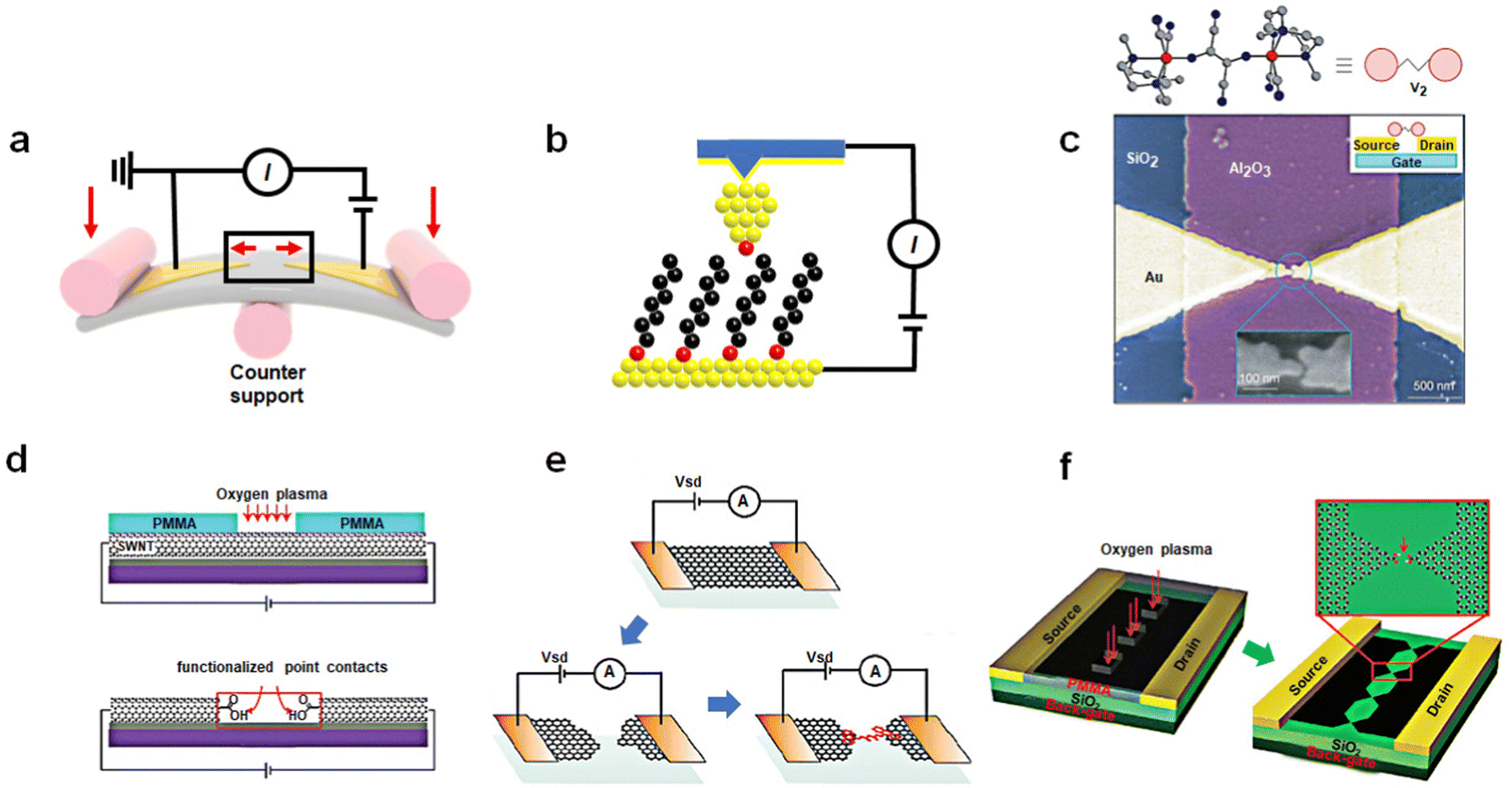 | ||
| Fig. 1 Preparation of single-molecule devices. (a) Schematic representation of the mechanically controllable break junction technique: two Au electrodes are stretched by mechanical forces to create nanoscale gaps. (b) Schematic representation of the scanning tunneling microscope break junction technique. The molecules deposited on the surface are picked up by the tip of STM. (c) Single-molecule FET devices using the electromigration break junction technique.36 Copyright: 2002, Macmillan Magazines Ltd. (d) Schematic representation of etching SWNTs by oxygen plasma into carboxylic acid-functionalized point contacts.40 Copyright: 2006, The AAAS. (e) Schematic representation of graphene single-molecule devices, formed by feedback-controlled electroburning.41 Copyright: 2011, ACS. (f) DLL strategy enables the fabrication of graphene triangle electrode arrays with nanogaps.42 Copyright: 2012, WILEY-VCH Verlag GmbH & Co. KGaA, Weinheim. | ||
Similar to a MCBJ, a scanning tunneling microscope break junction (STM-BJ) is a dynamic break junction (Fig. 1(b)).35 Picking up individual molecules deposited on the substrate surface through atomic sized tips, a molecule can construct a connection with the substrate and the tip simultaneously. This method can offer the advantage of simplicity and the ability to detect a multitude of surface atoms thousands of times over, yielding statistically sound conductivity results with excellent reproducibility. In addition, due to the ability of the STM technology to manipulate tip movement at the nanoscale and sensitivity in the z-direction, this approach facilitates the determination of molecular mechanical properties and the conductance changed with the length of molecules during stretching. However, the tip and the substrate mode pose a huge challenge for the production of integrated devices.
The advantages and disadvantages of STM-BJ and MCBJ technologies complement each other, making them an important platform for single-molecule electrical detection. Due to their similar working principles, it is expected that conductivity measurements of the same molecular system in similar environments will show good consistency.
Other methods using Au as electrodes to prepare single-molecule break junctions are as follows. Similar to the MCBJ, the method of electromigration break junctions is to use a gradually enlarged current to burn the gold wire.36 When a large electric current is passed through, the atoms in the gold electrodes will migrate, resulting in nanoscale gaps (Fig. 1(c)). Angular evaporation, online evaporation etching, and self-template masking methods all utilize nanoscale templates, either internal or external, in conjunction with traditional lithography and etching techniques.37–39 These methods allow for the production of nanoelectrodes smaller than the template size, followed by the construction of single-molecule junctions through molecular self-assembly. These methods need to improve the success rate of device fabrication to satisfy the requirements of integration.
It is worth noting that the aforementioned methods primarily employed gold as the electrode material, which has its drawbacks. Firstly, gold's high mobility can lead to atomic electromigration under the influence of bias voltage-generated electric fields, causing configuration changes, breakages, or short circuits. Secondly, gold can undergo non-specific adsorption with numerous molecules, resulting in the connection of unrelated molecules to the device, leading to noise signals. As a result, many tests need to be conducted in a vacuum environment. Lastly, metal atoms and molecules can form three types of connections: bridge, vertex, and triangle, each yielding distinct conductance properties.
SWCNTs represent a one-dimensional quantum material with a distinctive structure. The electrical properties of SWCNTs have been extensively studied, and in particular their electronic characteristics can be tuned into metallicity, offering an opportunity to create single-molecule junctions using SWCNT electrodes.40,49 This process involves coating the SWCNT surface with a layer of polymethyl methacrylate (PMMA) and employing high-resolution electron beam lithography (EBL) to produce ultra-small window precursors. Subsequently, oxygen plasma ion etching (RIE) is employed to etch the exposed SWCNT at these windows, producing nanogap electrodes with carboxyl-modified edges (Fig. 1(d)). Molecules featuring amino groups at both ends can be covalently linked to these electrodes through acylation reactions, yielding stable single-molecule junctions. It's worth noting that the size of these nanogaps can be precisely adjusted by varying the degree of oxidation, achieved by altering the exposure time under oxygen. Under optimized conditions, this method can achieve a success rate of approximately 20% to 25% in forming single-molecule connections.
Graphene, a two-dimensional semimetallic carbon material with a zero-bandgap, has played a pivotal role in various fields since its discovery. In comparison to SWCNTs, the mature technology for graphene production and transformation are well-established, providing the necessary infrastructure for incorporating graphene into single-molecule devices. Initially, the electrodes with nanoscale gaps in graphene can be achieved through feedback-controlled combustion methods (Fig. 1(e)).41 This involves employing a gradient current control based on feedback conductivity to burn away graphene. When the current decreases, the voltage is returned to zero, and the process is repeated to initiate a new voltage scan. The high-density current and Joule heat generated by applying a significant bias voltage leads to the oxidation and etching of graphene, gradually narrowing the graphene electrode to create nanoscale gaps. Molecules can then bridge between these graphene electrodes through π–π stacking interactions. However, the lack of precise control over the sites during this oxidation process makes the electric combustion method less predictable, resulting in unclear electrode configurations. To address this challenge, the dashed line lithography (DLL) strategy enables the fabrication of graphene triangle electrode arrays with nanogaps matched to the molecular scale (Fig. 1(f)).42,50 This method aims to create carboxylic acid-terminated graphene nanogap electrodes, which establish a reliable connection between the target molecule and the electrode. Initially, PMMA is spun onto the graphene surface to form a mask layer. Electron beam etching is then performed on each graphene device using a CAD file with a designed dashed line pattern. Oxygen plasma etching is employed to precisely etch the graphene bands along the exposed windows, resulting in a serrated point-to-point graphene nanogap point electrode array.
Comparison to dynamic break junctions, static single-molecule devices can achieve the field-effect transistor (FET) functionality through more intricate fabrication processes. The increased bond energy of the amide bond significantly enhances device stability, as evidenced by the high cycle numbers demonstrated in subsequent research on memristor model devices. However, the complexity of the preparation process has led to a moderate success rate for carbon-based single-molecule devices. Currently, the most critical challenge in this field is to improve the success rate of device preparation, particularly achieving integration for practical applications.
2.2 Preparation of a vertical molecular tunneling device
Over the past few decades, significant technological advancements have been realized in the field of electronics with functional monolayer devices, which have shown that a monolayer is sufficient to construct efficient charge transport channels. Monolayer devices can be categorized based on the direction of current transmission into two main types: vertical and horizontal monolayer devices.53,54 As horizontal devices primarily focus on charge transport properties between molecules within the film, while vertical devices manifest the device functionality determined by the tunneling properties of individual molecules, this article will emphasize vertical monolayer devices. A typical device structure comprises a bottom electrode, a self-assembled monolayer and a top electrode, as shown in Fig. 2(a). The construction of the bottom electrode involves the selection of the substrate (typically silicon or flexible substrates) and the preparation of the bottom electrode using techniques such as evaporation, spin coating, or transfer. Next, a monolayer is prepared on the bottom electrode through self-assembly, the conditions of which can vary based on the electrode material. The properties of the functional center of monolayer molecules, which act as charge transport channels, determine the performance of monolayer material devices. Since structural defects can significantly impact charge transport, it is imperative to create a highly ordered, defect-free monolayer structure. Self-assembled monolayers (SAMs) are organized molecular layers formed when active molecules attach to the surface of the bottom electrode via anchoring groups. Their thickness typically ranges from 1 nm to 3 nm and is determined by the length of the molecules. The formation of SAMs is a result of the anchoring groups of molecules binding to the substrate electrode to form a monolayer, while the molecules adsorbed through physical adsorption can be easily washed away. The advantages of this method include a straightforward process flow, low substrate shape dependence, and high stability (due to molecules binding chemically to the substrate and primarily interacting via van der Waals forces between molecular chains). As depicted in Fig. 2(a), SAMs can be segmented into two components: anchoring groups and functional groups. The anchoring groups bind to the substrate's reactive sites through chemical bonds. By altering the anchoring groups, the interaction strength between molecules and electrodes, influencing electron charge transfer difficulty, can be adjusted. The functional group serves as the central element for realizing the memristive function. It must meet two criteria: firstly, it should ensure that molecules are arranged in an orderly way on the substrate electrode via van der Waals interactions; secondly, it should maintain a stable bistable state under external conditions. SAMs are designed by considering both parts to meet specific application requirements. Finally, the top electrode is fabricated on the self-assembled monolayer. If necessary, modulation methods can be introduced, such as designing a transparent graphene top electrode to further incorporate a gate control or introduce an optical field.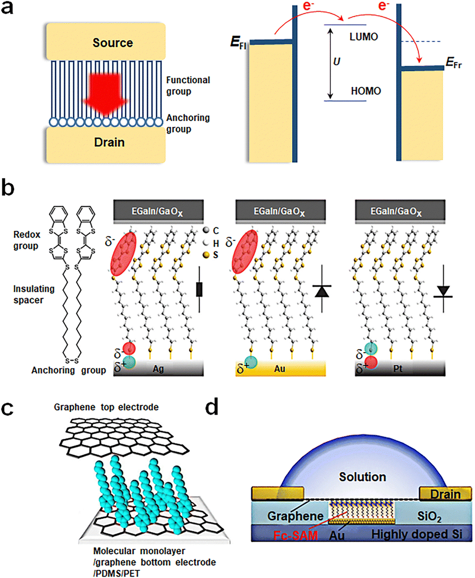 | ||
| Fig. 2 Preparation of vertical molecular tunneling devices. (a) Structure and mechanism of vertical molecular tunneling devices. (b) Schematic illustrations of junctions with M = Ag, Au, and Pt.51 Copyright: 2020, American Chemical Society. (c) Schematic of a transparent and flexible molecular monolayer junction between the two graphene electrodes.52 Copyright: 2013, Springer Nature Limited. (d) Schematic illustration of the device structure of Au/Fc-SAM/SLG junction with a liquid drop on top of the chip.30 Copyright: 2020, Elsevier Inc. | ||
Currently, single-molecule non-volatile memory devices can be fabricated through various methods; some representative examples are as follows. Fig. 2(b) showcases a traditional device fabrication method starting with a silicon wafer, followed by the preparation of metal electrodes through thermal or electron beam evaporation. Single molecules are anchored to metal electrodes via chemical bonds, such as disulfide bonds. Ultimately, the EGaIn electrode is transferred onto the self-assembled monolayer, with EGaIn being the most popular top electrode due to its low contact resistance and high stability.51Fig. 2(c) presents another fabrication approach, where graphene is employed for bottom and top electrodes. The graphene bottom electrode forms carbon–carbon bonds with aromatic diazonium salts chemically, while the top electrode binds to the molecular film via van der Waals forces. Compared to metal electrodes, graphene offers superior conductivity, chemical stability, thinness, flexibility, exceptional mechanical bendability, and translucency, which implies that SAMs can be more easily modulated by external fields such as light and force. Furthermore, the experiment utilizes flexible PDMS/PET as its substrate, enabling mechanical bending capabilities for the device.52 Lastly, Fig. 2(d) displays a more innovative design. This design involves depositing gold on etched conductive Si to serve as the bottom electrode, followed by further molecular assembly. Employing chemical vapor deposition (CVD) grown graphene as the top electrode provides exceptional transparency. The selective permeability of graphene ensures that devices can be regulated through external factors such as ion gates. This structure allows researchers to explore the relationship between Fermi levels and molecular orbital levels between molecules and graphene more conveniently and control the oxidation–reduction states of the molecule with ease.30 This innovative design paves the way for future molecular-scale non-volatile memories and holds promise as a vital direction for the future of electronics.
3. Molecular design and demonstration
In the realm of molecular electronics, alterations in the molecular structure often leads to changes of conductance. Certain molecules exhibit the bistability. There are specific barriers in the transitions between these bistable states, restricting the stochastic transition. Under specific conditions, the system can undergo a controlled transition from one stable state to another and remain in that state. Applying the opposite stimulus can restore the system to its original state. Under specific conditions, molecules can undergo structural changes in response to various external stimuli, settling into a static state. When an opposing external stimulus is applied, a greater amount of energy is required to surmount a barrier. This conductance hysteresis phenomenon is manifested within devices, potentially serving as a form of non-volatile memory.3.1 Conformational transformations
Conformational transformations typically demand relatively low potentials. The transformation between bistable structures is susceptible to thermal relaxation. As a result, the transformation of a bistable state needs an appropriate barrier. One well-studied molecule in this context is bipyridyl-dinitro oligophenylene-ethynylene dithiol (BPDN-DT).55–57 Various device methods have been employed to investigate BPDN-DT (Fig. 3(a)), yielding consistent outcomes and revealing pronounced hysteresis in the I–V curve. Two mechanisms have been proposed to elucidate these transitions: (i) molecular motion attributed to tilting or conformational transformations and (ii) bond fluctuations stemming from molecules tethered to gold surfaces, adhering or separating in a stochastic manner. In the case of three-terminal devices, such as single-molecule transistors constructed from BPDN-DT, the switching behavior is experimentally observed to be contingent on gate regulation. This suggests that the switching mechanism is founded on bias-induced molecular/electrode hybridization or bond angle alterations, rather than direct electronic processes like polaron formation. BPDN-DT single-molecule devices prepared using the MCBJ method exhibit increased cycle numbers and stability. Notably, “reading” and “erasure” experiments are conducted, affirming that this behavior is indeed an intrinsic property of the molecule. However, no hysteresis is detected when the molecule is replaced by BP-DT without nitro groups (Fig. 3(b)).57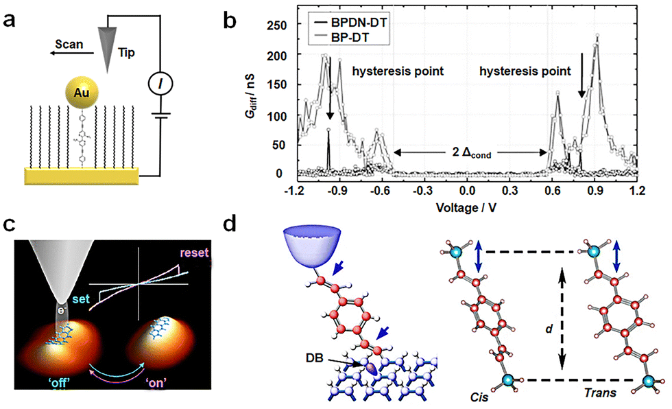 | ||
| Fig. 3 Diagram of the bistable transformation mechanism caused by conformational transformations. (a) Diagram of STM experiments. BPDN molecules are inserted into the C11 alkane matrix.55 Copyright: 2005, Springer Nature Limited. (b) Diagram of Gdiff–V data of BPDN-DT and BP-DT. Black arrows indicate the discontinuity in the BPDN-DT curve.57 (c) Schematic diagram of reversible conformational changes of ADT at different voltages.58 Copyright: 2015, American Chemical Society. (d) Schematic diagram of conformation changes of DEB by mechanical force.59 Copyright: 2015 Macmillan Publishers Limited. | ||
In addition, the pentaphenyl analog anthrthiophene (ADT) demonstrates a fully reversible binary switch between different adsorption conformations on metal surfaces with charge transfer (Fig. 3(c)).58 In the low conduction state (off state), the ADT molecule adopts a curved adsorption geometry, with the propylene ring situated close to the Cu (111) surface, and the LUMO orbital partially occupied. By applying a substantial negative bias voltage pulse, the ADT molecule transforms into a planar structure (on state), moving away from the substrate. This leads to a decrease in the energy of the LUMO orbital and the opening of a conductive window.
Apart from bias as an external stimulus, mechanical forces can also induce reversible tautomeric changes in double bonds. Using scanning tunneling microscopy (STM) to anchor para-diacetylene benzene (DEB) between silicon components to form Si/single-molecule/Si structures, a robust covalent bond forms between the molecule and the silicon electrode (Fig. 3(d)).59 This enables stable and repetitive control of the molecule's conformation through a mechanical force. Although the DEB molecule itself is symmetrical, the double bond formed after anchoring to the silicon electrode imparts asymmetry. When the two double bonds are positioned on the same side, a cis configuration is achieved, while opposite positions result in a trans conformation. When stretched along the z-axis, the DEB structure transitions from cis to trans, with the distance between the compression tip and the base changing back to cis. Calculation shows that the DEB conductance primarily relies on the energy level of the LUMO. The trans structure, characterized by a greater distance, exhibits a lower LUMO orbital energy which is closer to the Fermi level than the cis structure, consequently yielding higher conductance values.
3.2 Tautomerisms
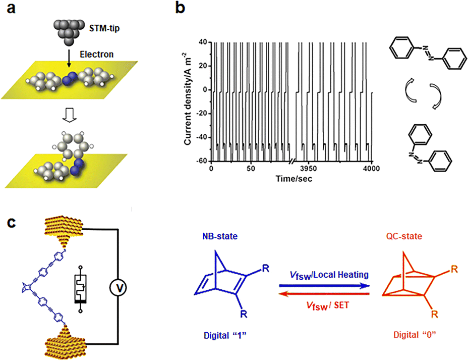
Azobenzene has been the subject of extensive studies concerning cis/trans tautomerisms of its N![[double bond, length as m-dash]](https://www.rsc.org/images/entities/char_e001.gif) N bonds.60–62 Under ultraviolet light irradiation, azobenzene undergoes a transformation from a trans-configuration to a cis-configuration. It can revert to the trans-state under visible light or thermal excitation. In STM imaging experiments involving azobenzene (Fig. 4(a)), it is observed that in its initial state, azobenzene molecule exhibits a dumbbell shape on the Au surface.63 Upon applying a −1.5 V bias, the image transitions into a circular point, accompanied by an increase in conductance, indicating the cis-configuration. Reversing this to the trans state is achieved by applying a +2.5 V bias. A monolayer composed of azobenzene derivatives is deposited between two reduced graphene oxide (rGO) electrodes, enabling the creation of a non-volatile memory on a flexible substrate (Fig. 4(b)).64 The molecule made soft contact with the graphene electrode sheet. Changes in voltage induced cis–trans isomerization of the molecule, resulting in different groups making contact with the rGO electrode. Specifically, the cis NN bond came into closer proximity to the rGO electrode, while the trans configuration used the hydrophobic CF3 group. The “writing”, “reading”, and “erasure” voltages are determined to be 3.0 V, −1.0 V, and −3.0 V, respectively. The memory operation exhibited stability over more than 400 cycles. The switching ratio, exceeding 20, is sustained for a retention time surpassing 10
N bonds.60–62 Under ultraviolet light irradiation, azobenzene undergoes a transformation from a trans-configuration to a cis-configuration. It can revert to the trans-state under visible light or thermal excitation. In STM imaging experiments involving azobenzene (Fig. 4(a)), it is observed that in its initial state, azobenzene molecule exhibits a dumbbell shape on the Au surface.63 Upon applying a −1.5 V bias, the image transitions into a circular point, accompanied by an increase in conductance, indicating the cis-configuration. Reversing this to the trans state is achieved by applying a +2.5 V bias. A monolayer composed of azobenzene derivatives is deposited between two reduced graphene oxide (rGO) electrodes, enabling the creation of a non-volatile memory on a flexible substrate (Fig. 4(b)).64 The molecule made soft contact with the graphene electrode sheet. Changes in voltage induced cis–trans isomerization of the molecule, resulting in different groups making contact with the rGO electrode. Specifically, the cis NN bond came into closer proximity to the rGO electrode, while the trans configuration used the hydrophobic CF3 group. The “writing”, “reading”, and “erasure” voltages are determined to be 3.0 V, −1.0 V, and −3.0 V, respectively. The memory operation exhibited stability over more than 400 cycles. The switching ratio, exceeding 20, is sustained for a retention time surpassing 10![[thin space (1/6-em)]](https://www.rsc.org/images/entities/char_2009.gif) 000 seconds in this memory device. Even after more than 20000 readouts over a period of 10000 seconds, the device consistently exhibits distinct ON/OFF states and nondestructive states.
000 seconds in this memory device. Even after more than 20000 readouts over a period of 10000 seconds, the device consistently exhibits distinct ON/OFF states and nondestructive states.
 | ||
| Fig. 4 Diagram of the bistable transformation mechanism caused by tautomerisms. (a) A concept of electron-induced isomerization of an azobenzene adsorbed onto a metallic surface with a scanning tunneling microscope.63 Copyright: 2006 American Physical Society. (b) The current responses of write-read-erase-read performances at 3, −1, −3, and −1 V with 2 s of pulse width time.64 Copyright: 2013, WILEY-VCH Verlag GmbH & Co. KGaA, Weinheim. (c) Schematic depiction of the single-molecule device with a modulating bias and the mechanism of conduction changes.27 Copyright: 2020 Wiley-VCH Verlag GmbH & Co. KGaA, Weinheim. | ||
Norbornene (NB) can be photoisomerized in traditional photochemical experiments.65,66 When a single norbornene molecule is connected between electrodes, tautomerisms can also occur to form quadricyclane (QC) structures under electrical stimulation (Fig. 4(c)).27,67 NB structures with higher conjugation exhibit greater conductance than QC structures. The forward transformation from NB to QC is thermally activated by an electrically heated junction, while the reverse process necessitates a high bias voltage and single electron transfer (SET) between the molecule and the gold contact to induce reverse isomerization. By adjusting the bias between the two switching potentials, both reactions can be controlled reversibly in situ. Writing NB is achieved by applying a high bias voltage of 0.75 V, reading requires a bias of 0.1 V, and erasure back to QC is accomplished by applying a bias of 0.25 V.
3.3 Intramolecular motions
Fullerene molecules possess the remarkable ability to encapsulate various metal atoms within their cage-like structures to form endohedral metallofullerenes (EMFs).68–70 Evidence suggests that atoms or clusters of atoms enclosed within fullerenes maintain certain motions within the limited space of the cage. Numerous external factors can influence this internal motion at the molecular level, subsequently affecting the properties of the molecule. Utilizing a low-temperature ultra-high vacuum scanning tunneling microscope (UHV-STM), researchers have discovered that Tb@C82 can exhibit switching and memory functions by adjusting the position of Tb atoms within the molecule (Fig. 5(a)).71 When Tb@C82 is deposited on an Au (111) substrate coated with self-assembled monolayers of octylmercaptan, scanning tunnel spectroscopy (STS) reveals hysteresis in Tb@C82 characterized by negative differential conductivity (NDC). This hysteresis phenomenon arises from the disparities in dipole moments resulting from different Tb atom positions within the carbon cage. When a bias voltage is applied, a stronger electric field intensity is required to flip the dipole moments. Ce@C82 has also been shown to exhibit noticeable hysteresis in single-molecule transistor devices, affecting the regulation of gate voltage on conductance (Fig. 5(b)).72 Applying a voltage (VSD) to the source–drain electrode greater than 84 mV results in nearly equal source and drain capacitances. As a large bias voltage is applied, the I–V curve exhibits hysteresis, with drain capacitance increasing and gate capacitance decreasing as VG increases. In addition, the hysteresis of fullerene inclusion complexes can be regulated not only by bias voltage but also by gate voltage. Gd@C82 serves as a single-molecule electret in non-volatile memory applications (Fig. 5(c)).73 In contrast to Ce@C82, when a fixed source–drain bias voltage is applied, two sets of alternating Coulomb oscillation modes emerge. Density functional theory calculations reveal the corresponding atomic configurations of the two switchable states, with the Gd atom located on two adjacent six-membered rings, marked with red and blue hexagons, respectively. The energy difference between these states is 6.1 meV, making it susceptible to external electric field-induced switching. Furthermore, using Sc2C2@Cs(hept)-C88 as the core molecule enables not only information writing and erasure at room temperature but also demonstrates fourteen Boolean logic operations (Fig. 5(d)).74 According to theoretical calculations, switching between the two dipole states of the fullerene inclusion complex is non-spontaneous at 300 K and can be achieved by applying ±0.8 V with a switching time of less than 0.15 ms. This represents a significant advancement toward room temperature electric manipulation, low power consumption, and dual-purpose memory logic devices. The conversion mechanism is illustrated below in Fig. 5(d). There exists a barrier impeding the transition between bistable states. The system is initially in state I and is not subject to random transformation into state II by thermal activation. Upon the application of a stimulus, such as a positive electric field (writing voltage), the transformation barrier decreases as the energy of state I increases, facilitating the transition from state I to state II. Conversely, applying the opposite energy, such as a negative electric field (erasure voltage), increases the energy of state II, prompting the system to switch from state II to state I. When the stimulus is at an intermediate level (reading voltage), the state remains unchanged, thereby achieving a non-volatile memory function.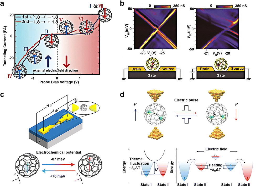 | ||
| Fig. 5 Diagram of the bistable transformation mechanism caused by motion of inset in EMF. (a) Schematic representation of single-molecule switches of Tb@C82 that describes hysteresis and NDC caused by the interaction between its electric dipole moment and an external electric field.71 Copyright: 2005, American Chemical Society. (b) Coulomb stability diagrams of a Ce@C82 single-molecule transistor measured (left) before and (right) after the large bias voltage inducing the hysteretic behavior is applied. The schematic illustrations of possible molecular configurations for two states are showed below, respectively.72 Copyright: AIP Publishing. (c) Schematic representation of single-molecule electret of Gd@C82 using the electromigration break junction technique. The dipole moment of molecule is regulated by the gate voltages.73 Copyright: 2020, Springer Nature Limited. (d) Molecular structures and energy level diagrams of the Sc2C2@Cs(hept)-C88 device.74 Copyright: 2022, Springer Nature Limited. | ||
Mechanical interlocking molecular architectures, exemplified by rotaxane and catenane, can exhibit bistable properties.75–77 These molecules offer intriguing possibilities for designing memory function molecules by utilizing redox reactions to reversibly transform between several stable structures.78 [2]catenane, for instance, is assembled using a combination of components, including tetrathiofulvalene (TTF), a 1,5-dioxynaphthalene ring system (NP) and two bipyridine units.79 Monolayer composed of this compound have been found to exhibit I–V hysteresis upon testing, paving the way for the development of non-volatile memory devices. The switching mechanism is depicted in Fig. 6(a), and the TTF group undergoes formation of structure [B]. When the voltage is reduced to close to zero, the co-configuration [B+0] is established with the reduction of TTF, representing an oxidation achieved by applying a −2 V bias voltage, leading to a Coulomb repulsion with two bipyridine units, resulting in the low-conductivity state (with a reading voltage of 0.1 V). The bipyridine ring is further reduced by application of a +2 V bias voltage, regenerating it into the [A0] structure. It is important to note that thermal relaxation is required during this cycle, limiting the device's operation to temperatures above 220 K. In addition to catenanes, memory devices based on [2]rotaxanes following principles have also been introduced, featuring a capacity of 160000 bits (Fig. 6(b)).80 These cross-bar memories are assembled with 400 silicon nanowires serving as the bottom electrode (16 nm wide, 33 nm spacing; doped with phosphate), passing over 400 Ti nanowire electrodes (16 nm wide, 33 nm spacing) (Fig. 6(c)). A single layer of bistable [2]rotaxane is sandwiched between these two nanowires. Despite the presence of numerous defects in the circuit, these defects can be easily identified through electronic testing and isolated using software coding. In addition, the signal retention time measured for this device (90 ± 40 minutes; median decay 75 minutes) is statistically equivalent to the rate reported for much larger and more well-characterized devices (58 ± 5 minutes).80
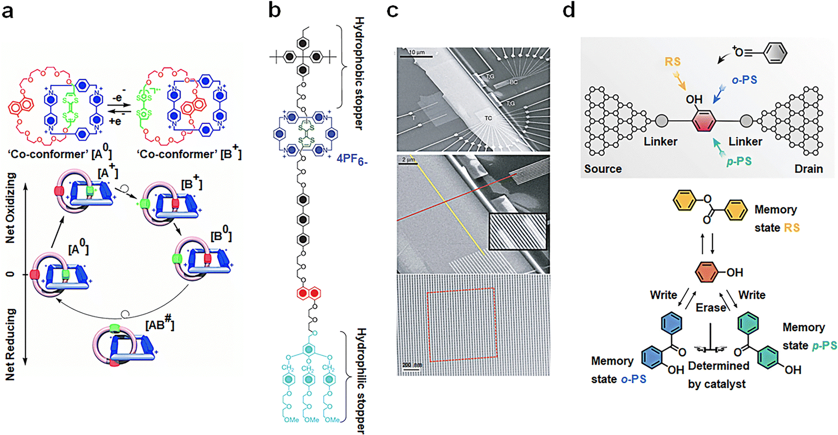 | ||
| Fig. 6 Diagram of the bistable transformation mechanism caused by the motion of mechanical interlocking molecular architectures and reaction. (a) Controlled by voltage regulation, [2]catenanes transfer reversibly between bistable states.79 Copyright: 2000, AAAS. (b) Structural formula of the bistable [2]rotaxane used in the crossbar memory. (c) Image of the entire circuit. [2]rotaxanes are deposited between two orthogonal nanowires.80 Copyright: 2007, Springer Nature Limited. (d) Schematic diagram of memristors based on a Fries rearrangement reaction. The rearrangement of p-PS and o-PS products can be controlled by electric field direction.81 Copyright: 2022, Wiley-VCH GmbH. | ||
A single-molecule memristor is proposed, designed around the concept of dynamic structure reconstruction powered by an electric field (Fig. 6(d)).81 The functional core of this memristor consists of phenyl acetate, which is tethered between graphene point electrodes via an amide bond. The inclusion of a PDMS package serves to prevent the escape of acetyl groups and enhances the device's operational lifespan. The key principle at play here is the reversible Fries rearrangement, which allows the acetyl group to be strategically positioned in the ortho–para-position of the hydroxyl or benzene ring, all under the influence of an electric field. Initially, the memristor is in a stable RS(PS) state, but this state can be effectively erased by applying a bias pulse of +0.6 V (−0.6 V) and rewritten to PS(RS) by employing a bias of −0.05 V (+0.05 V). The performance of this covalently connected solid-state single-molecule memristor is remarkable. It has demonstrated its capabilities by successfully undergoing more than 2000 high-frequency write–erase operations within a mere 10 seconds, showcasing the stability of resistance switching through structural reconstruction.
3.4 Spin changes
The spin state of a molecule represents the spin characteristics of all electrons within the molecule.83,84 The electron spin state affects the electronic structure of the molecule, subsequently influencing the conductivity of the molecule. Recent advancements have delved into measuring and manipulating spins at the nanoscale, even down to the single-molecule level. Utilizing distinct molecular spin states as the design principle for single-molecule non-volatile memory devices is an emerging research frontier. This concept is grounded on the premise of using the electron spin in molecules as the unit of information memory, leveraging spin interactions between molecules and transitions between spin states for memories. Two primary research approaches exist: one based on the intrinsic spin states of the molecule and the other involves altering the spin injection properties of the electrode.Single-molecule magnets (SMMs) exhibit magnetic behavior similar to macroscopic magnets. Typically, these molecules possess one or more unpaired electron spins, which can interact and result in the overall magnetic properties of the molecule. Since the late last century, when magnetic hysteresis of SMMs was observed, there have been numerous reports on studying molecular magnetic features using SMMs on various substrates. Nonetheless, a fundamental challenge lies in the elusive preservation of molecular magnetic hysteresis evidence when SMMs interface with metal surfaces, substantially hampering their integration into electronic devices. Roberta Sessoli's group designed a sulfur-functionalized derivative, [Fe4(L)2(dpm)6], which self-assembles into a monolayer on the Au surface (Fig. 7(a) and (b)). This Fe4 molecule, consisting of four high-spin iron(III) ions, exhibits a propeller-like molecular structure. The outer four Fe spins (S = 5/2) interact antiferromagnetically with the inner Fe spin resulting in a ground spin (S = 5) state characterized by an anisotropy barrier of about 16 K.32 For the first time, the hysteresis behavior of pure molecular SMMs on a non-magnetic Au electrode is observed. Although integrating SMMs into non-volatile memory devices still faces challenges like low operational temperatures, this study underscores the potential of SMMs to achieve magnetic bistability. Building on this research, one can envision using other means to alter the bistability of the molecule, such as the possibility of controlling magnetization reversal in the electrode–molecule–electrode nanostructure via conducting electrons.
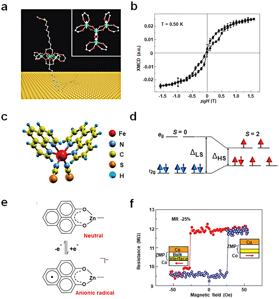 | ||
| Fig. 7 Diagram of the bistable transformation mechanism caused by spin changes. (a) Schematic diagram of the Fe4 anchoring on a gold surface. (b) Hysteresis and magnetization dynamics of the Fe4 monolayer.32 Copyright: 2009, Springer Nature Limited. (c) Three-dimensional model of a Fe-phen molecule. (d) Simplified electronic configuration of the Fe(II) 3d states in the ligand field.82 Copyright: 2012, The Author(s). (e) Zinc methyl phenalenyl (ZMP) transitions from a neutral state with no spin to a charged radical with a magnetic moment upon interaction with a ferromagnet surface. (f) Magnetoresistance measurements of a device with a single ferromagnetic electrode.33 Copyright: 2013, Springer Nature Limited. | ||
Beyond SMMs, spin-crossover (SCO) molecules can be used to prepare memories between low-spin (LS) and high-spin (HS) states upon external stimuli like temperature, light, pressure, magnetic or electric fields, or charge flow. As shown in Fig. 7(c) and (d) a prototypical SCO complex, Fe(1,10-phenanthroline)2(NCS)2 molecules (Fe-phen), undergoes a spin transition around 175 K, accompanied by changes in Fe–N bond distances and angles. At this temperature, the splitting energy between eg and t2g decreases, causing the Fe-phen molecule to transition from a LS (S = 0) state to a high-spin HS (S = 2) state.82 This study, at low temperatures (≈4.6 K), employed STM to probe the spin states and conductance of single Fe-phen molecules. The results revealed coexistence of HS and LS states for Fe-phen molecules adsorbed on a Cu (100) surface. However, strong coupling of the NCS group with the substrate prevented spin-state writing via voltage. Introducing an interfacial CuN layer to weaken the interaction between the molecule and the metal interface successfully achieved a spin-crossover transition at the single-molecule level through applied voltage. The research results reveal that the molecule transits from the LS state to the HS state at 3.0 V. In the HS state, with a delay of 1.4 seconds after voltage removal, there is a slight decrease in current, leading to a return to the LS state and achieving a bistable transition.
Altering the spin-injection properties of the electrode is an important method for achieving molecular spin changes. As illustrated in Fig. 7(e) and (f), the neutral molecule C14H10O2Zn (ZMP) possesses no net spin. However, when grown on a ferromagnetic surface, spin transfer at the interface facilitates the formation of a hybrid organic–metal supermagnetic layer, exhibiting significant magnetic anisotropy and spin-filtering properties. This interfacial layer produces spin-associated resistance, displaying interface magnetoresistance (IMR) effects at room temperature.33 This chemical modification at the interface arises from interactions between molecular orbitals and ferromagnetic d-orbital. These interactions yield new interface states, altering the electronic and magnetic properties of the molecule. These effects largely depend on the specific molecular structure and morphology, influencing spin polarization and spin injection efficiency. The ZMP molecule's geometric configuration allows for strong overlap between d and p orbitals, triggering d–p hybridization effects. The IMR response offers an effective means to detect and modulate the spin states of magnetic molecules, paving the way for advancements in molecular memory technology at room temperature.
3.5 Charge changes
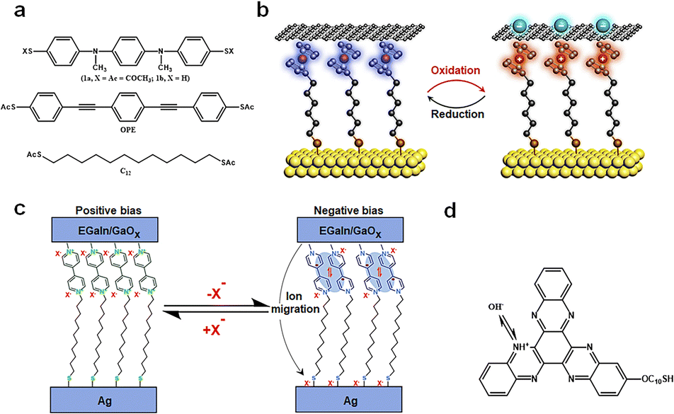
Redox-active molecules, due to their intrinsic charge changes, have showcased their unique potential in energy storage, presenting an avant-garde platform for nanoscale memory research studies.29 High spatial resolution and precision in charge transfer are vital for single-molecule redox reactions. The architecture of single-molecule devices should be designed to ensure precise and controllable conditions for charge change and transfer. The charge states within the device can be modulated by external fields, predominantly through source–drain charge capture and redox processes regulated by the gate. It is noteworthy that these molecules exhibit relative stability across their various redox states, providing an added layer of reliability for real-world applications. In addition, post redox reactions, these molecules typically induce certain alterations in the device structure, such as molecular dimerization, ion migration, protonation, and interactions between the molecules and electrodes. It is imperative for readers to discern these nuances, as we believe that these modifications play a supplementary role in device functionality.Introducing redox groups into molecules is an effective means to achieve bistable conductance in single-molecule devices. Compared to C12 and OPE molecules (Fig. 8(a)), the top molecule has a redox section, and a distinct redox peak appears in the cyclic voltammetry (CV) test. To construct a comprehensive electronic apparatus, these nanowires are meticulously positioned between two larger gold electrodes, resulting in a sandwiched electrode–molecule–electrode configuration. These molecules, under ambient conditions, exhibit repeatable bistable switching characteristics, signifying their capability to toggle reversibly between two distinct states in memories.85 Further empirical investigations revealed the molecules’ cyclic voltammograms, showcasing two pronounced single-electron redox peaks. These reversible chemical transitions are likely correlated with the observed reversible switching characteristics in these conductors, suggesting that toggling the molecule's redox state can switch its conductive state. This process encompasses charge capture, where charges traverse from the source to the drain, instigating a shift in the molecular charge state. Specifically, when a potential difference is applied across the electrodes, charges migrate from one electrode to the other. During this transition, charges initially permeate the connected molecule and are either captured or released by the molecule's redox center. This dynamic sequence culminates in redox reactions, effectuating the molecular conductive state switch.
 | ||
| Fig. 8 Diagram of the bistable transformation mechanism caused by charge changes. (a) Molecules that were incorporated into the in-wire junctions studied here.85 Copyright: 2005, American Chemical Society. (b) Schematic illustration of the Au/Fc-SAM/SLG junction with oxidation and reduction treatments.30 Copyright: 2020, Elsevier Inc. (c) Schematic and mechanism illustration of MV junctions.86 Copyright: 2020, The Author(s), under exclusive licence to Springer Nature Limited. (d) The molecular formula for S-C10-HATNA.31 Copyright: 2022, The Author(s), under exclusive licence to Springer Nature Limited. | ||
In the research as shown in Fig. 8(b), the authors harnessed a graphene-based vertical monolayer heterostructure to craft a tri-terminal molecular redox switch device. Initially, a monolayer of 6-ferrocenylhexanethiol (referred to as FcC6S) is formed on an Au/highly-doped Si substrate, which serves as the source electrode. Subsequently, a monolayer of graphene, cultivated through the CVD method, was transferred onto this SAM, acting as the drain electrode. When a 0.1 M HClO4 solution was introduced as the electrolyte, covering both the FcC6S and the gate electrode, the graphene's tight encapsulation of the FcC6S enabled the reversible modulation of electrochemical redox reactions within the graphene layer. It is noteworthy that during the oxidation of FcC6S, when it transitions into a cationic state, an electrostatic repulsion arises between it and graphene, leading to an increased separation between them.30 This electrostatic interplay plays a pivotal role during the redox processes, significantly facilitating the formation of bistability in the memories.
The process of redox reactions generating free radicals may be accompanied by the occurrence of side reactions, further facilitating the formation of high and low conductance states (Fig. 8(c)). MV (methylviologen), in its initial state, is characterized by a dicationic configuration, represented as MV2+. When subjected to a specific external stimulus, it undergoes a transformation, evolving into a radical cation, denoted as MV˙+. However, this state isn’t the molecule's final resting phase. The MV˙+ radical cation experiences an additional dimerization process, eventually leading to the formation of a stable [MV˙+]2 complex. This intricate dimerization is driven by π–π stacking interactions, a phenomenon where aromatic rings stack atop one another due to dispersive forces, and electron spin pairing, which refers to the coupling of unpaired electron spins. Simultaneously, as the molecule undergoes these transformations, there is a need to stabilize the charge that has been introduced into the molecule.
This necessitates an ion migration mechanism. During this phase, excess counter-ions, which are ions that balance the charge of the molecule, make their way to the positively charged bottom electrode. It is crucial to highlight the significance of the counter ion size in this mechanism.86 The dimensions of these counter ions have a profound impact on the efficiency of the dimerization process. Furthermore, they play a decisive role in determining the overall stability of the molecular switch and its operational efficiency. The interplay between the redox processes, dimerization, and ion migration underscores the intricate nature of the MV-based tunneling mechanism and its potential implications in nanoscale memory applications.
Multi-step redox reactions can result in multiple conductance states A particular example is the hexaazatrinaphthylene (HATNA) terminus that readily undergoes six successive proton coupled electron transfer (PCET) steps for dynamic covalent N–H bond formation (Fig. 8(d)). This switch is integrated into a tunneling junction buttressed by a SAM, wherein the terminal parts of the SAM molecule are designed to facilely undergo six consecutive PCET steps. The authors, through CV tests, demonstrated that the SAM underwent sequential PCET with stable intermediates, laying the groundwork for its emulation of synaptic behaviors. Density functional theory (DFT) calculations elucidated the electronic structure of SAM, revealing the impact of the oxidation and protonation states of HATNA on the SAM's electronic structure.31 This electronic structural shift is intrinsically tied to the redox processes, providing a theoretical foundation for the switch's dynamic behavior. Through their unique charge handling mechanisms at the nanoscale, redox-active molecules achieve efficient and stable charge states, with the molecule's redox states and associated chemical reactions playing a pivotal role in non-volatile memories.
4. Conclusions and outlook
Non-volatile memory stands as a foundational element in contemporary logical operations and data memory. Molecular non-volatile memories, harnessed through molecular electronics, have displayed immense potential due to their exceptional performance. In the realm of molecular electronics, the presence of bistable state is a vital requirement for molecules to function effectively as non-volatile memories. In addition, the memristor can be defined as being able to accomplish functions like “writing”, “erasure”, “reading”, and even more advanced logical operations. This review primarily delves into the elucidation of preparation procedures for commonly utilized single-molecule electronic devices and monolayer electronic devices. It also involves an assessment of the advantages and drawbacks associated with various device types. The research efforts have involved the collection and classification of previously documented non-volatile memories or molecules exhibiting hysteresis phenomena between bistable states. The overarching goal is to provide insights and solutions to guide future molecular design and the preparation of devices.The conductivity of molecules is correlated with their structure, including the configuration, conformation, electronic structure, electronic spin and redox state. The transformation between bistable states typically aligns with reversible structural alterations. Achieving non-volatility necessitates the existence of a specific potential barrier between transitions of bistability. From a microscopic perspective, state changes can be categorized into several types, including conformational transformations, tautomerisms, intramolecular motions, spin changes, and charge changes. Conformational transformations primarily involve the rotation of single bonds and distortion of the ring. However, due to the low conversion barriers involved, the conformation changes of most molecules are disordered. Only a limited number of molecules exhibit bistable states. Tautomeric transformations primarily include the Z/E transition of double bonds and tautomeric changes in molecules like norbornene. The intramolecular motions in EMFs, mechanically interlocked molecular architectures, and Fries rearrangement reactions play a significant role. Fullerene inclusion complexes are controlled by an applied electric field and mechanically interlocked molecular architectures use electrostatic forces between intermolecular functional groups. Redox-active molecules are capable of capturing and releasing electrons under the influence of external voltage, maintaining a relatively stable state, which lays the foundation for non-volatile memories. In addition, certain molecules undergo structural changes during charge changes, such as molecular dimerization and ion migration, which play a supplementary role in device functionality. Exploring how to utilize the spin state of single-molecule electrons for information storage and retrieval is a significant direction for future developments in this field. Both single-molecule magnets and spin-crossover molecules have demonstrated unique magnetic behaviors, which can be modulated by external stimuli. Furthermore, the spin-injection characteristics of the electrode are of paramount significance.
Despite substantial progress, the molecule non-volatile memory faces challenges that necessitate the development of new strategies. One of the primary challenges we face is the fabrication of stable and dependable single-molecule devices. Although numerous techniques exist for creating these devices, achieving stability, reliability and reproducibility has proven to be a daunting task. Enhancements in the fabrication of single-molecule devices, including the adoption of novel electromigration or etching methods, hold the promise for increasing the production of single-molecule junctions and enabling the creation of device arrays. Single-molecule devices relying on metal electrodes face issues with stability, as they can be susceptible to damage caused by atomic migration of the electrodes. Given the remarkable stability of carbon materials, such as carbon nanotubes and graphene, these materials are being explored as alternative electrode materials. In addition, there is room for improvement in the way single molecules are connected. Introducing dependable anchor groups through molecular design or establishing strong chemical bonds can significantly enhance the stability of single-molecule devices. Furthermore, there is a need for the design of a greater variety of molecules with bistable state structures. While molecules of diverse structures have been discovered, many of the conductance changes resulting from molecular structural alterations exhibit randomness and disorder. It is essential to develop more experimental assays that enable high-throughput screening of molecules at the single-molecule level. It should be mentioned that current research studies on single-molecule memristors mainly focus on the realization of storage functions, with limited explorations of practical application concerns such as service life, erase/writing time, and energy consumption. Another critical issue of integrating single-molecule memristors remains a key challenge in this field and in the broader domain of single-molecule science. Overcoming these challenges will require significant breakthroughs and advances in the overarching field of single-molecule science. In addition, theoretical calculations can serve as valuable tools to complement experiments and confirm whether a molecule possesses a bistable state. The development of an improved theoretical model to guide experiments is of paramount importance. In summary, advancing research in single-molecule non-volatile memories necessitates collaborative efforts across multiple fields to achieve the goal of practical applications for molecular non-volatile memories.
Author contributions
X. F. G., C. C. J., W. S. and J. H. L. conceived the main concept of the review article. W. S. and J. H. L. collected the related information needed in writing the paper. W. S., J. H. L., G. W. L., C. C. J. and X. F. G. wrote and modified the manuscript. All authors discussed and commented on the manuscript.Conflicts of interest
There are no conflicts to declare.Acknowledgements
We are grateful to the National Key R&D Program of China (2021YFA1200102, 2021YFA1200101, and 2022YFE0128700), the National Natural Science Foundation of China (22173050, 22150013, 21727806, and 21933001), the New Cornerstone Science Foundation through the XPLORER PRIZE, the Natural Science Foundation of Beijing (2222009), the Beijing National Laboratory for Molecular Sciences (BNLMS202105), the Fundamental Research Funds for the Central Universities (63223056), and the “Frontiers Science Center for New Organic Matter” at Nankai University (63181206).Notes and references
- B. H. Park, B. S. Kang, S. D. Bu, T. W. Noh, J. Lee and W. Jo, Nature, 1999, 401, 682–684 CrossRef CAS
.
- E. X. Wu, Y. Xie, S. J. Wang, D. H. Zhang, X. D. Hu and J. Liu, Nano Res., 2020, 13, 3445–3451 CrossRef CAS
- M. Bagheri, M. Poot, M. Li, W. P. H. Pernice and H. X. Tang, Nat. Nanotechnol., 2011, 6, 726–732 CrossRef CAS PubMed
- K. Asadi, D. M. De Leeuw, B. De Boer and P. W. M. Blom, Nat. Mater., 2008, 7, 547–550 CrossRef CAS PubMed
- B. Mukherjee, A. Zulkefli, K. Watanabe, T. Taniguchi, Y. Wakayama and S. Nakaharai, Adv. Funct. Mater., 2020, 30, 2001688 CrossRef CAS
- R. J. Luyken and F. Hofmann, Nanotechnology, 2003, 14, 273–276 CrossRef CAS
- S. G. Hahm, S. Choi, S. H. Hong, T. J. Lee, S. Park, D. M. Kim, W. S. Kwon, K. Kim, O. Kim and M. Ree, Adv. Funct. Mater., 2008, 18, 3276–3282 CrossRef CAS
- W. L. Leong, P. S. Lee, A. Lohani, Y. M. Lam, T. Chen, S. Zhang, A. Dodabalapur and S. G. Mhaisalkar, Adv. Mater., 2008, 20, 2325–2331 CrossRef CAS
- M. Kaltenbrunner, P. Stadler, R. Schwödiauer, A. W. Hassel, N. S. Sariciftci and S. Bauer, Adv. Mater., 2011, 23, 4892–4896 CrossRef CAS PubMed
- Y. B. Li, Z. R. Wang, R. Midya, Q. F. Xia and J. J. Yang, J. Phys. D: Appl. Phys., 2018, 51, 503002 CrossRef
- D. B. Strukov, G. S. Snider, D. R. Stewart and R. S. Williams, Nature, 2008, 453, 80–83 CrossRef CAS PubMed
- R. Haight, W. Haensch and D. Friedman, Science, 2016, 353, 124–125 CrossRef CAS PubMed
- G. Wetzstein, A. Ozcan, S. Gigan, S. H. Fan, D. Englund, M. Soljacic, C. Denz, D. A. B. Miller and D. Psaltis, Nature, 2020, 588, 39–47 CrossRef CAS PubMed
- T. Kempitiya, S. Sierla, D. De Silva, M. Yli-Ojanperä, D. Alahakoon and V. Vyatkin, Appl. Energy, 2020, 280, 115918 CrossRef
- A. D. Bartolomeo, H. Rücker, P. Schley, A. Fox, S. Lischke and K. Y. Na, Solid State Electron., 2009, 53, 644–648 CrossRef
- Y. Guo, C. Yang, S. Zhou, Z. Liu and X. Guo, Adv. Mater., 2022, 34, 2004827 Search PubMed
- P. Li, Y. Chen, B. Wang, M. Li, D. Xiang, C. Jia and X. Guo, Opto-Electron. Adv., 2022, 5, 210094 CAS
- Z. H. Liu, X. X. Li, H. Masai, X. Y. Huang, S. Tsuda, J. Terao, J. L. Yang and X. F. Guo, Sci. Adv., 2021, 7, eabe4365 CrossRef CAS PubMed
- A. R. Champagne, A. N. Pasupathy and D. C. Ralph, Nano Lett., 2005, 5, 305–308 CrossRef CAS PubMed
- H. Y. Fu, X. Zhu, P. H. Li, M. M. Li, L. Yang, C. C. Jia and X. F. Guo, J. Mater. Chem. C, 2022, 10, 2375–2389 RSC
- Y. H. Wang, F. Yan, D. F. Li, Y. F. Xi, R. Cao, J. F. Zheng, Y. Shao, S. Jin, J. Z. Chen and X. S. Zhou, J. Phys. Chem. Lett., 2021, 12, 758–763 CrossRef CAS PubMed
- D. Xiang, H. Jeong, D. Kim, T. Lee, Y. J. Cheng, Q. L. Wang and D. Mayer, Nano Lett., 2013, 13, 2809–2813 CrossRef CAS PubMed
- K. Moth-Poulsen and T. Bjornholm, Nat. Nanotechnol., 2009, 4, 551–556 CrossRef CAS PubMed
- H. Song, Y. Kim, Y. H. Jang, H. Jeong, M. A. Reed and T. Lee, Nature, 2009, 462, 1039–1043 CrossRef CAS PubMed
- X. M. Xie, P. H. Li, Y. X. Xu, L. Zhou, Y. H. Yan, L. H. Xie, C. C. Jia and X. F. Guo, ACS Nano, 2022, 16, 3476–3505 CrossRef CAS PubMed
- Z. Chen, C. L. Ho, L. Wang and W. Y. Wong, Adv. Mater., 2020, 32, e1903269 CrossRef PubMed
- H. B. Li, B. E. Tebikachew, C. Wiberg, K. Moth-Poulsen and J. Hihath, Angew. Chem., Int. Ed., 2020, 59, 11641–11646 CrossRef CAS PubMed
- R. Marin, G. Brunet and M. Murugesu, Angew. Chem., Int. Ed., 2021, 60, 1728–1746 CrossRef CAS PubMed
- Y. Han and C. A. Nijhuis, Chem. – Asian J., 2020, 15, 3752–3770 CrossRef CAS PubMed
- C. Jia, I. M. Grace, P. Wang, A. Almeshal, Z. Huang, Y. Wang, P. Chen, L. Wang, J. Zhou, Z. Feng, Z. Zhao, Y. Huang, C. J. Lambert and X. Duan, Chem, 2020, 6, 1172–1182 CAS
- Y. Wang, Q. Zhang, H. P. A. G. Astier, C. Nickle, S. Soni, F. A. Alami, A. Borrini, Z. Zhang, C. Honnigfort, B. Braunschweig, A. Leoncini, D.-C. Qi, Y. Han, E. del Barco, D. Thompson and C. A. Nijhuis, Nat. Mater., 2022, 21, 1403–1411 CrossRef CAS PubMed
- P. H. Li, Y. J. Chen, B. Y. Wang, M. M. Li, D. Xiang, C. C. Jia and X. F. Guo, Opto-Electron. Adv., 2022, 5, 210094 CAS
- K. V. Raman, A. M. Kamerbeek, A. Mukherjee, N. Atodiresei, T. K. Sen, P. Lazić, V. Caciuc, R. Michel, D. Stalke, S. K. Mandal, S. Blügel, M. Münzenberg and J. S. Moodera, Nature, 2013, 493, 509–513 CrossRef CAS PubMed
- M. A. Reed, C. Zhou, C. J. Muller, T. P. Burgin and J. M. Tour, Science, 1997, 278, 252–254 CrossRef CAS
- X. D. Cui, A. Primak, X. Zarate, J. Tomfohr, O. F. Sankey, A. L. Moore, T. A. Moore, D. Gust, G. Harris and S. M. Lindsay, Science, 2001, 294, 571–574 CrossRef CAS PubMed
- W. Liang, M. P. Shores, M. Bockrath, J. R. Long and H. Park, Nature, 2002, 417, 725–729 CrossRef CAS PubMed
- S. Kubatkin, A. Danilov, M. Hjort, J. Cornil, J.-L. Brédas, N. Stuhr-Hansen, P. Hedegård and T. Bjørnholm, Nature, 2003, 425, 698–701 CrossRef CAS PubMed
- L. Qin, S. Park, L. Huang and C. A. Mirkin, Science, 2005, 309, 113–115 CrossRef CAS PubMed
- J. Tang, Y. Wang, J. E. Klare, G. S. Tulevski, S. J. Wind and C. Nuckolls, Angew. Chem., Int. Ed., 2007, 46, 3892–3895 CrossRef CAS PubMed
- X. Guo, J. P. Small, J. E. Klare, Y. Wang, M. S. Purewal, I. W. Tam, B. H. Hong, R. Caldwell, L. Huang, S. O’Brien, J. Yan, R. Breslow, S. J. Wind, J. Hone, P. Kim and C. Nuckolls, Science, 2006, 311, 356–359 CrossRef CAS PubMed
- F. Prins, A. Barreiro, J. W. Ruitenberg, J. S. Seldenthuis, N. Aliaga-Alcalde, L. M. K. Vandersypen and H. S. J. Van Der Zant, Nano Lett., 2011, 11, 4607–4611 CrossRef CAS PubMed
- Y. Cao, S. Dong, S. Liu, L. He, L. Gan, X. Yu, M. L. Steigerwald, X. Wu, Z. Liu and X. Guo, Angew. Chem., Int. Ed., 2012, 51, 12228–12232 CrossRef CAS PubMed
- K. Ullmann, P. B. Coto, S. Leitherer, A. Molina-Ontoria, N. Martín, M. Thoss and H. B. Weber, Nano Lett., 2015, 15, 3512–3518 CrossRef CAS PubMed
- P. Gehring, A. Harzheim, J. Spièce, Y. Sheng, G. Rogers, C. Evangeli, A. Mishra, B. J. Robinson, K. Porfyrakis, J. H. Warner, O. V. Kolosov, G. A. D. Briggs and J. A. Mol, Nano Lett., 2017, 17, 7055–7061 CrossRef CAS PubMed
- A. K. Feldman, M. L. Steigerwald, X. Guo and C. Nuckolls, Acc. Chem. Res., 2008, 41, 1731–1741 CrossRef CAS PubMed
- C. Jia, B. Ma, N. Xin and X. Guo, Acc. Chem. Res., 2015, 48, 2565–2575 CrossRef CAS PubMed
- Q. Xu, G. Scuri, C. Mathewson, P. Kim, C. Nuckolls and D. Bouilly, Nano Lett., 2017, 17, 5335–5341 CrossRef CAS PubMed
- C. Yang, Y. Guo, S. Zhou, Z. Liu, Z. Liu, D. Zhang and X. Guo, Adv. Mater., 2023, 35, 2209750 CrossRef CAS PubMed
- W. Ren, J. R. Reimers, N. S. Hush, Y. Zhu, J. Wang and H. Guo, J. Phys. Chem. C, 2007, 111, 3700–3704 CrossRef CAS
- C. Yang, C. Yang, Y. Guo, J. Feng and X. Guo, Nat. Protoc., 2023, 18, 1958–1978 CrossRef CAS PubMed
- Y. Han, M. S. Maglione, V. Diez Cabanes, J. Casado-Montenegro, X. Yu, S. K. Karuppannan, Z. Zhang, N. Crivillers, M. Mas-Torrent, C. Rovira, J. Cornil, J. Veciana and C. A. Nijhuis, ACS Appl. Mater. Interfaces, 2020, 12, 55044–55055 CrossRef CAS PubMed
- S. Seo, M. Min, S. M. Lee and H. Lee, Nat. Commun., 2013, 4, 1920 CrossRef PubMed
- J. Shin, J. S. Eo, T. Jeon, T. Lee and G. Wang, Adv. Sci., 2022, 9, 1500205 Search PubMed
- D. Xiang, X. L. Wang, C. C. Jia, T. Lee and X. F. Guo, Chem. Rev., 2016, 116, 4318–4440 CrossRef CAS PubMed
- A. S. Blum, J. G. Kushmerick, D. P. Long, C. H. Patterson, J. C. Yang, J. C. Henderson, Y. Yao, J. M. Tour, R. Shashidhar and B. R. Ratna, Nat. Mater., 2005, 4, 167–172 CrossRef CAS PubMed
- Z. K. Keane, J. W. Ciszek, J. M. Tour and D. Natelson, Nano Lett., 2006, 6, 1518–1521 CrossRef CAS PubMed
- E. Lörtscher, J. W. Ciszek, J. Tour and H. Riel, Small, 2006, 2, 973–977 CrossRef PubMed
- B. Borca, V. Schendel, R. Pétuya, I. Pentegov, T. Michnowicz, U. Kraft, H. Klauk, A. Arnau, P. Wahl, U. Schlickum and K. Kern, ACS Nano, 2015, 9, 12506–12512 CrossRef CAS PubMed
- M. Nakamura, S. Yoshida, T. Katayama, A. Taninaka, Y. Mera, S. Okada, O. Takeuchi and H. Shigekawa, Nat. Commun., 2015, 6, 8465–8473 CrossRef CAS PubMed
- A. Goulet-Hanssens, M. Utecht, D. Mutruc, E. Titov, J. Schwarz, L. Grubert, D. Bléger, P. Saalfrank and S. Hecht, J. Am. Chem. Soc., 2017, 139, 335–341 CrossRef CAS PubMed
- A. Staubitz, M. Walther, W. Kipke, S. Schultzke and S. Ghosh, Synthesis, 2021, 1213–1228 CrossRef
- M. Yamauchi, K. Yokoyama, N. Aratani, H. Yamada and S. Masuo, Angew. Chem., Int. Ed., 2019, 58, 14173–14178 CrossRef CAS PubMed
- B.-Y. Choi, S.-J. Kahng, S. Kim, H. Kim, H. W. Kim, Y. J. Song, J. Ihm and Y. Kuk, Phys. Rev. Lett., 2006, 96, 156106 CrossRef PubMed
- M. Min, S. Seo, S. M. Lee and H. Lee, Adv. Mater., 2013, 25, 7045–7050 CrossRef CAS PubMed
- E. E. Bonfantini and D. L. Officer, J. Chem. Soc., Chem. Commun., 1994, 12, 1445–1446 RSC
- H. Löfås, B. O. Jahn, J. Wärnå, R. Emanuelsson, R. Ahuja, A. Grigoriev and H. Ottosson, Faraday Discuss., 2014, 174, 105–124 RSC
- B. E. Tebikachew, H. B. Li, A. Pirrotta, K. Börjesson, G. C. Solomon, J. Hihath and K. Moth-Poulsen, J. Phys. Chem. C, 2017, 121, 7094–7100 CrossRef CAS PubMed
- T. Tsuchiya, R. Kumashiro, K. Tanigaki, Y. Matsunaga, M. O. Ishitsuka, T. Wakahara, Y. Maeda, Y. Takano, M. Aoyagi, T. Akasaka, M. T. H. Liu, T. Kato, K. Suenaga, J. S. Jeong, S. Iijima, F. Kimura, T. Kimura and S. Nagase, J. Am. Chem. Soc., 2008, 130, 450–451 CrossRef CAS PubMed
- W. Shen, L. Zhang, S. Zheng, Y. Xie and X. Lu, ACS Appl. Mater. Interfaces, 2017, 9, 28838–28843 CrossRef CAS PubMed
- X. Lu, L. Feng, T. Akasaka and S. Nagase, Chem. Soc. Rev., 2012, 41, 7723–7760 RSC
- Y. Yasutake, Z. Shi, T. Okazaki, H. Shinohara and Y. Majima, Nano Lett., 2005, 5, 1057–1060 CrossRef CAS PubMed
- N. Okamura, K. Yoshida, S. Sakata and K. Hirakawa, Appl. Phys. Lett., 2015, 106, 043108 CrossRef
- K. Zhang, C. Wang, M. Zhang, Z. Bai, F.-F. Xie, Y.-Z. Tan, Y. Guo, K.-J. Hu, L. Cao, S. Zhang, X. Tu, D. Pan, L. Kang, J. Chen, P. Wu, X. Wang, J. Wang, J. Liu, Y. Song, G. Wang, F. Song, W. Ji, S.-Y. Xie, S.-F. Shi, M. A. Reed and B. Wang, Nat. Nanotechnol., 2020, 15, 1019–1024 CrossRef CAS PubMed
- J. Li, S. Hou, Y.-R. Yao, C. Zhang, Q. Wu, H.-C. Wang, H. Zhang, X. Liu, C. Tang, M. Wei, W. Xu, Y. Wang, J. Zheng, Z. Pan, L. Kang, J. Liu, J. Shi, Y. Yang, C. J. Lambert, S.-Y. Xie and W. Hong, Nat. Mater., 2022, 21, 917–923 CrossRef CAS PubMed
- J. Zhao, Z. Zhang, L. Cheng, R. Bai, D. Zhao, Y. Wang, W. Yu and X. Yan, J. Am. Chem. Soc., 2022, 144, 872–882 CrossRef CAS PubMed
- R. Da Silva Rodrigues and K. M. Mullen, ChemPlusChem, 2017, 82, 814–825 CrossRef CAS PubMed
- N. Pearce, M. Tarnowska, N. J. Andersen, A. Wahrhaftig-Lewis, B. S. Pilgrim and N. R. Champness, Chem. Sci., 2022, 13, 3915–3941 RSC
- A. H. Flood, E. W. Wong and J. F. Stoddart, Chem. Phys., 2006, 324, 280–290 CrossRef CAS
- C. P. Collier, G. Mattersteig, E. W. Wong, Y. Luo, K. Beverly, J. Sampaio, F. M. Raymo, J. F. Stoddart and J. R. Heath, Science, 2000, 289, 1172–1175 CrossRef CAS PubMed
- J. E. Green, J. Wook Choi, A. Boukai, Y. Bunimovich, E. Johnston-Halperin, E. Deionno, Y. Luo, B. A. Sheriff, K. Xu, Y. Shik Shin, H.-R. Tseng, J. F. Stoddart and J. R. Heath, Nature, 2007, 445, 414–417 CrossRef CAS PubMed
- Y. Guo, C. Yang, S. Zhou, Z. Liu and X. Guo, Adv. Mater., 2022, 34, 2204827 CrossRef CAS PubMed
- T. Miyamachi, M. Gruber, V. Davesne, M. Bowen, S. Boukari, L. Joly, F. Scheurer, G. Rogez, T. K. Yamada, P. Ohresser, E. Beaurepaire and W. Wulfhekel, Nat. Commun., 2012, 3, 938 CrossRef PubMed
- A. R. Rocha, V. M. García-Suárez, S. W. Bailey, C. J. Lambert, J. Ferrer and S. Sanvito, Nat. Mater., 2005, 4, 335–339 CrossRef CAS PubMed
- J. R. Friedman and M. P. Sarachik, Annu. Rev. Conder. Matter Phys., 2010, 1, 109–128 CrossRef CAS
- L. T. Cai, M. A. Cabassi, H. Yoon, O. M. Cabarcos, C. L. McGuiness, A. K. Flatt, D. L. Allara, J. M. Tour and T. S. Mayer, Nano Lett., 2005, 5, 2365–2372 CrossRef CAS PubMed
- Y. Han, C. Nickle, Z. Zhang, H. Astier, T. J. Duffin, D. Qi, Z. Wang, E. Del Barco, D. Thompson and C. A. Nijhuis, Nat. Mater., 2020, 19, 843–848 CrossRef CAS PubMed
Footnote |
| † W. S. and J. H. L. contributed equally to this review. |
| This journal is © The Royal Society of Chemistry 2024 |