
Theoretical investigation of width effects in the electronic and transport properties of carbon nanoribbons with 5-8-5 carbon rings: a first-principles study†
Elder Augusto Viana
Mota
 *ab,
Carlos Alberto Brito
da Silva
Jr
c and
Jordan
Del Nero
d
*ab,
Carlos Alberto Brito
da Silva
Jr
c and
Jordan
Del Nero
d
aPós-Graduação em Física, Universidade Federal do Pará, Belém, PA 66075-110, Brazil. E-mail: elder.mota@icen.ufpa.br
bFaculdade de Ciências Exatas e Tecnologia, Universidade Federal do Pará, 68440-000, Abaetetuba, PA, Brazil
cFaculdade de Física, Universidade Federal do Pará, Ananindeua, PA 67113-901, Brazil
dFaculdade de Física, Universidade Federal do Pará, Belém, PA 66075-110, Brazil
First published on 3rd January 2024
Abstract
In this work, we theoretically investigated the effect of width on the energetic stability, and structural, electronic and transport properties of five carbon nanoribbons (three zigzag and two armchair) with 5-8-5 carbon ring symmetry based on 2D POPGraphene, to understand how the width can tune their features and to suggest possible applications in nanoelectronics. Our study was conducted via Density Functional Theory (DFT) implemented in the SIESTA package, to compute the energetic, structural, and electronic properties, and DFT combined with the non-equilibrium Green's function, to compute the transport properties. The results show that all the nanoribbons are stable, with cohesive energy values in the range of those of several carbon allotropes. Furthermore, we see that the stability increases with the width, strongly depends on edge terminations (penta-rings improve stability), and reaches values similar to those of 2D POPGraphene. The structural properties show that the width effect associated with edge shape acts like a uniaxial tensile strain application in most of the nanoribbons. The electronic properties show that most of the nanoribbons are metallic, except for the two armchair cases, which have a tiny indirect bandgap. We see that the armchair cases have several sub-bandgap regions that trigger negative differential resistance in devices, and this possibly suggests applications in optoelectronic devices. These regions decrease with increasing width. The transport properties show that the zigzag devices in general have Field Effect Transistor (FET) or Resonant Tunneling Diode (RTD) behaviour, and the armchair ones show FET, RTD and Zener diode behaviour. Therefore, the width of a carbon nanoribbon can be used to adjust its features, which consequently suggests several applications of this kind of material in nanoelectronics.
1 Introduction
Carbon allotropes are frequently applied in the areas of science and technology due to their great properties, such as thermal stability, mechanical resistance and the quantum Hall effect.1–4 Among the carbon allotropes predicted so far, graphene has attracted special attention since its experimental achievement in 2004 by Geim and Novoselov.5 Graphene is a 2D carbon allotrope with sp2 hybridization, and presents interesting features, such as massless behaviour of its electrons, high thermal stability, and the quantum Hall effect.6 However, despite all these outstanding features, due to its hexagonal symmetry and lack of a band-gap, the application of graphene in Li-ion batteries and nanoelectronics is difficult.7–10Several researchers have been searching for new 2D carbon allotropes with other ring symmetries, to break the hexagonal symmetry of graphene and uncover new properties.11–15 For instance, in 2015, Fan et al. proposed a family of 2D carbon allotropes with 5-, 6-, and 8-carbon rings named α-, β-, and γ-PHOGraphene (Penta-Hexa-Octa-Graphene).16 With different properties to graphene, these carbon allotropes present metallic or semiconducting behavior, depending on the arrangement of the 5-, 6-, and 8-carbon rings, and have possible applications as anode materials in Li-ion batteries.17
We also cite the work of Wang et al.18 in 2019, which proposed a carbon allotrope with 5-, 6-, and 8-carbon rings named XGraphene. Different from graphene, this carbon allotrope presents a negative Poisson ratio, which suggests applications in the field of auxetic materials.19,20
Besides the interest in 2D carbon materials, several works have also been investigating the properties of carbon nanoribbons,21,22 mainly for applications in nanoelectronics.23–25 Such materials are interesting because they have a large range of modification methods that can be implemented to tune their properties26–28 and consequently their device behavior and applications.
For instance, in 2014, Dai et al.29 proposed and investigated carbon nanoribbons based on TGraphene, a 2D carbon allotrope with 4- and 8-carbon rings.30 In their work, they investigated the influence of the edge shape on the electronic and transport properties of this kind of nanoribbon, showing that zigzag nanoribbons present a metallic behavior, and armchair ones present a number of Dirac cones depending on the nanoribbon width.
In 2015, Yuan et al.31 investigated the edge-shape effect in carbon nanoribbons based on the PHAGraphene structure.13 They showed that the spin edge states are strongly dependent of the edge configuration, suggesting applications for these nanoribbons in spin valves.
In 2016, Rajbanshi et al.32 proposed a carbon nanoribbon based on a 2D carbon allotrope with pentagonal symmetry and carbon atoms with sp2 and sp3 hybridization, named pentagraphene.33 Their work shows that these nanoribbons are stable and mechanically flexible, tolerating up to 11.5% axial strain. Furthermore, analysing the width effect, they saw that wider nanoribbons show interesting charge separation, and the band gap of the wider ribbons opens up the possibility of a stable nanoribbon with a large band gap for applications in optoelectronic devices.
Based on experimental evidence of a 5-5-8 defect line in graphene sheets,34–36 Wang et al.37 conducted theoretical work and predicted the existence of a 2D carbon allotrope with a 5-8-5-carbon ring symmetry, named POPGraphene (Penta-Octa-Penta-Graphene – POPG), which was predicted to have low energy and possess great dynamic, thermal and mechanical stability. Due to its great features, it was suggested to be applied as an anode material in Li-ion batteries, with fast charge/discharge rates.
Since the prediction of POPG structures, several works have investigated their properties and applications as nanotubes38 and membranes,39 analyzed the edge shape and hydrogen edge passivation effect in the corresponding carbon nanoribbons,40,41 and also proposed analogous structures like POP-nitro-graphene.42 However, the effect of width on the electronic and transport properties of POPG nanoribbons has not been investigated yet in the literature.
There are several works in the literature that strongly suggest that the width can change the structural and electronic properties of a nanoribbon.26,29,43,44 For instance, Bang et al.44 conducted experimental work in 2018, where they investigated the width effect in graphene nanoribbons. In their work, they designed Field Effect Transistors (FETs) based on graphene on Si substrates, for several widths, and demonstrated (for instance) that the on/off current ratio is inversely proportional to ribbon width.
Since carbon nanoribbons are interesting materials with promising applications in nanoelectronics, and a complete investigation of all parameters that can change nanoribbons’ features are necessary to define the range of applications of these materials, in this work we investigated the effect of width on the electronic and transport properties of POPGraphene nanoribbons (POPGNRs) to fully understand the possible applications of these materials in nanoelectronics. We first investigated the feasibility of experimental achievement of these nanoribbons via cohesive energy values, and then we analyzed the effect of width on the structural, electronic and transport properties of these materials.
2 Methodology
We proposed nanoribbons based on POPG structures. To define them, we investigated all the possible different edge configurations in the zigzag (zz) and armchair (ac) directions as defined for the 2D POPG structure,37 using the same shape at the top and bottom.41 The chosen zz and ac cutting orientation is also justified by the electronic properties (see Fig. 3 and 4 for an insight), which show the same pattern in the zz and ac directions. This approach lets us define five kinds of nanoribbons: zzPOPGNR with a penta-ring edge shape bonded to one hydrogen (zzPOPGNR-P1), zzPOPGNR with an octa-ring edge shape (zzPOPGNR-O), zzPOPGNR with a penta-ring edge shape bonded to two hydrogens (zzPOPGNR-P2), acPOPGNR with a penta-ring edge shape (acPOPGNR-P), and acPOPGNR with a mix of penta-rings and octa-rings on the edges (acPOPGNR-PO). The width (W) of the nanoribbons was defined based on the octa-rings (1 octa-ring = 1 unit of width), and the adopted nomenclature was chosen based on this definition (see Fig. 1), for instance: (N,W)zzPOPGNR-P1 means a zzPOPGNR-P1 type ribbon with width W, replicated N-times in the periodic direction. In this work, the width was varied from one (W = 1) to five (W = 5) for the investigation of the structural and electronic properties, and from one (W = 1) to four (W = 4) for the transport properties.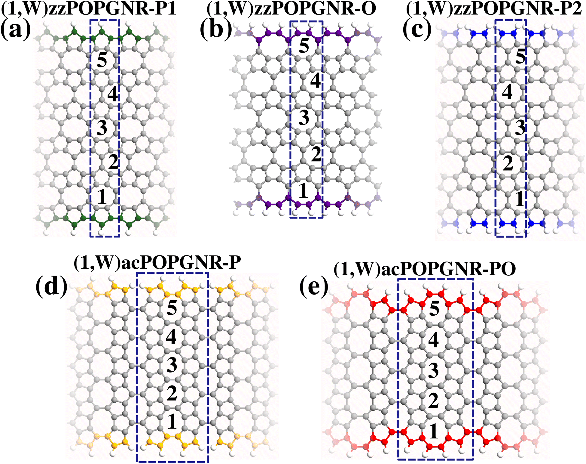 | ||
| Fig. 1 POPGraphene nanoribbons. (a) zzPOPGNR-P1, (b) zzPOPGNR-O, (c) zzPOPGNR-P2, (d) acPOPGNR-P and (e) acPOPGNR-PO. Colored carbon atoms highlight the edge shape of the nanoribbons. The dashed rectangle in (a)–(e) delimits the nanoribbon unit cell and the numbers (1 to 5) represent the nanoribbon width (based on the octa-rings). | ||
The nanoribbon unit cells were optimized using density functional theory (DFT) methodology45–47 implemented in the SIESTA package.48 A k-mesh of 65×1×1 was chosen to solve the integrals in the Brillouin zone for the zz nanoribbons, and 25×1×1 for the ac ones, besides a mesh cutoff of 360 Ry for the zz nanoribbons and 420 Ry for the investigated ac systems.
The Generalized-Gradient-Approximation (GGA) approach of Perdew, Burke and Ernzerhof (PBE)49 was used to represent the exchange correlation effects. The valence electrons were represented using the double-ζ-polarized basis set (DZP), and the pseudopotentials of Troullier and Martins with Kleinman–Bylander projectors were chosen to represent the inner ones. An energy shift of 40 meV was set to define the pseudo atomic orbital range.
The conjugated-gradient (CG) method was implemented to optimize the unit cell until the force tolerance between the atoms and the stress tensor component of the unit cell were less than 0.005 eV Å−1 and 0.01 GPa, respectively.
The electronic transport was conducted using the non-equilibrium Green's function method combined with DFT in the TranSIESTA package.50–52 The molecular device was designed using a two-terminal model (source = left lead and drain = right lead), with two unit-cell replications for the left and right leads, besides five replications for the scattering region, in the zigzag cases (nine unit cells in total – (9,W), see Fig. 5(a), 6(a), and 7(a)), and one unit cell for the left and right lead, besides three unit-cell replications, for the armchair ones (five unit cells in total – (5,W), see Fig. 8(a) and 9(a)).
A bias voltage was applied in the range of −1.0 V to 1.0 V, and the transport properties were obtained with the TBTrans tool from the SIESTA package, using the Landauer-Büttiker formalism:53
 | (1) |
 | (2) |
| T(E,V) = Tr[ΓL(ε)G†(ε)ΓR(ε)G(ε)] | (3) |
3 Results & discussion
3.1 Energetic stability and structural properties
The width confinement could generate instabilities in the structures, since the atoms on the edges have a degree of freedom in the tailored direction. Thus, to verify that the investigated nanoribbons in this work are energetically stable, we first calculate the cohesive energy (Ecoh) by the equation: | (4) |
The results for all the investigated nanoribbons are presented in Fig. 2, where we can see that all the proposed nanoribbons are stable, since all energies obtained are negative. Furthermore, we see that zzPOPGNR-P1 is remarkably the most stable among them, for all widths, with highly negative values in the range of approximately 8.08 eV/atom to 8.59 eV/atom (variation of 0.51 eV/atom – ΔEcoh = 0.51 eV/atom), followed by acPOPGNR-P, which has an energy range of approximately 7.39 eV/atom to 8.31 eV/atom (ΔEcoh = 0.92 eV/atom). The zzPOPGNR-P2 and acPOPGNR-PO cases have approximately the same energy for N ≥ 3, but zzPOPGNR-P2 is more stable than acPOPGNR-PO for N ≤ 2. zzPOPGNR-O is the least stable nanoribbon, with an energy variation between −6.63 eV/atom and −8.21 eV/atom (ΔEcoh = 1.58 eV/atom).
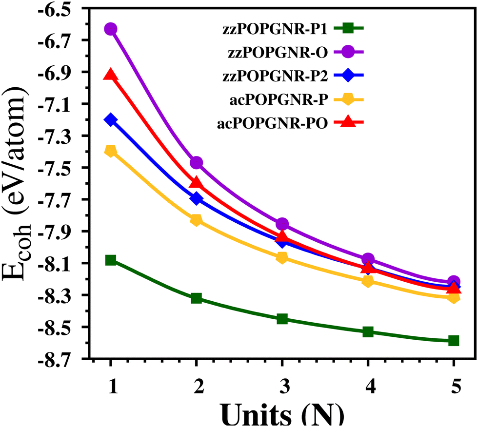 | ||
| Fig. 2 Cohesive energy as a function of width for the investigated nanoribbons. | ||
We can also see that zzPOPGNR-P1 has minor energy variation with the width increase (stable behavior), since it shows a small change of 0.51 eV/atom from N = 1 to N = 5 in relation to the other nanoribbons, which show variation of about 1.0 eV/atom. Furthermore, these results strongly suggest that the most stable nanoribbons are those with penta-ring termination, since they have minor Ecoh values.
These results are in good agreement with the literature for carbon nanoribbons,31,32 showing that they are, for instance, more stable than some of the proposed tetragraphene nanoribbons in the work of Vasconcelos et al.26
The structural properties that minimize the total energy (which was used to calculate the Ecoh presented in Fig. 2) are also different from the bulk POPG parameters due to the width effects. Thus, we analyzed the effect of width on the bond length and lattice constant of all nanoribbons investigated; these are presented in Tables 1 and 2 (lattice constant and bond length, respectively).
| Lattice constant (Å) | |||||
|---|---|---|---|---|---|
| NR | zzPOPGNR-P1 | zzPOPGNR-O | zzPOPGNR-P2 | acPOPGNR-P | acPOPGNR-PO |
| N = 1 | 3.7138 | 3.7674 | 3.9282 | 9.2709 | 9.3128 |
| N = 2 | 3.7124 | 3.7382 | 3.8393 | 9.2482 | 9.2075 |
| N = 3 | 3.7127 | 3.7300 | 3.8079 | 9.2079 | 9.2345 |
| N = 4 | 3.7138 | 3.7261 | 3.7884 | 9.1942 | 9.2139 |
| N = 5 | 3.7132 | 3.7242 | 3.7732 | 9.1827 | 9.1951 |
| Bond length (Å) | |||||
|---|---|---|---|---|---|
| NR | zzPOPGNR-P1 | zzPOPGNR-O | zzPOPGNR-P2 | acPOPGNR-P | acPOPGNR-PO |
| N = 1 | 1.407–1.479 | 1.409–1.458 | 1.356–1.517 | 1.389–1.477 | 1.403–1.511 |
| N = 2 | 1.407–1.481 | 1.397–1.477 | 1.341–1.486 | 1.395–1.490 | 1.400–1.480 |
| N = 3 | 1.404–1.480 | 1.396–1.472 | 1.337–1.481 | 1.400–1.479 | 1.388–1.487 |
| N = 4 | 1.405–1.479 | 1.393–1.470 | 1.411–1.478 | 1.402–1.476 | 1.389–1.483 |
| N = 5 | 1.406–1.480 | 1.394–1.471 | 1.330–1.473 | 1.400–1.476 | 1.389–1.475 |
Table 1 shows that for the zz cases, all lattice-constant values are higher than the POPG bulk value (a = 3.6833 Å).37 We see that zzPOPGNR-P1 (second column in Table 1) has lattice-constant values closest to the bulk value and zzPOPGNR-P2 (fourth column in Table 1) has the most distant ones.
For the zzPOPGNR-P1 case, the lattice constant remains approximately constant (with just a small variation in the third decimal place for the N = 2 and N = 3 cases) with the width increase. This is in good agreement with the cohesive energy results (Fig. 2), which show a small energy variation with the increase in the width. For the zzPOPGNR-O (third column in Table 1) and zzPOPGNR-P2 cases, we see that the values decrease with the width increase, tending towards the bulk values. These results show that the zzP1 edge shape does not drastically change the material structure for all the widths, but for the zzO and zzP2 edge-shape case, the width effect acts like uniaxial tensile strain application in the nanoribbon, since the nanoribbon lattice constant increases (relative to the 2D POPG) for lower widths. This effect is more remarkable in the zzP2 case.
For the ac cases (fifth and sixth columns in Table 1), we see that the values are higher than the POPG bulk value (b = 9.1124 Å).37 We can see that acPOPGNR-P has values closest to that of the bulk and that in general, the lattice parameters for both ac types decrease, tending towards the bulk values (except for (1,3)acPOPGNR-PO, which shows an increase with the width increase). These results show that the edge shape with the width effect acts like uniaxial tensile strain application, since the nanoribbon length increase for lower widths. This effect is more pronounced for the acPO nanoribbons than for the acP ones, since we have lattice-constant values that are more distant from the 2D POPG case for this kind of nanoribbon.
We can see from Table 2 that there is not a great change in the bond length range with the increase in width for each kind of nanoribbon, since there is just a small difference between the minimum and maximum values. The zzPOPGNR-P1 type has a medium bond length variation in the range of approximately 1.406 Å to 1.480 Å, for the zzPOPGNR-O type it is in the range of 1.398 Å to 1.470 Å, for zzPOPGNR-P2 it is in the range of 1.355 Å to 1.487 Å, for acPOPGNR-P it is in the range of 1.397 Å to 1.480 Å, and for acPOPGNR-PO it is in the range of 1.394 Å to 1.487 Å. We can see that these bond length results explain the lattice-constant values, including the abnormal value for the (1,3)acPOPGNR-PO case, since they show that the nanoribbon lattice constant increases (against the decreasing tendency for the other nanoribbon widths for this type) due to the increase (of 0.007 Å) in the bond length for this nanoribbon width. Furthermore, we see that these results show that the structures are in an sp2-like configuration and are in good agreement with the literature for carbon allotropes.13,14
3.2 Electronic properties
To analyze the effect of the edge shape and quantum confinement on the electronic properties, we plot the band structure (BS) and the density of states (DOS) for all the nanoribbons (Fig. 3 and 4).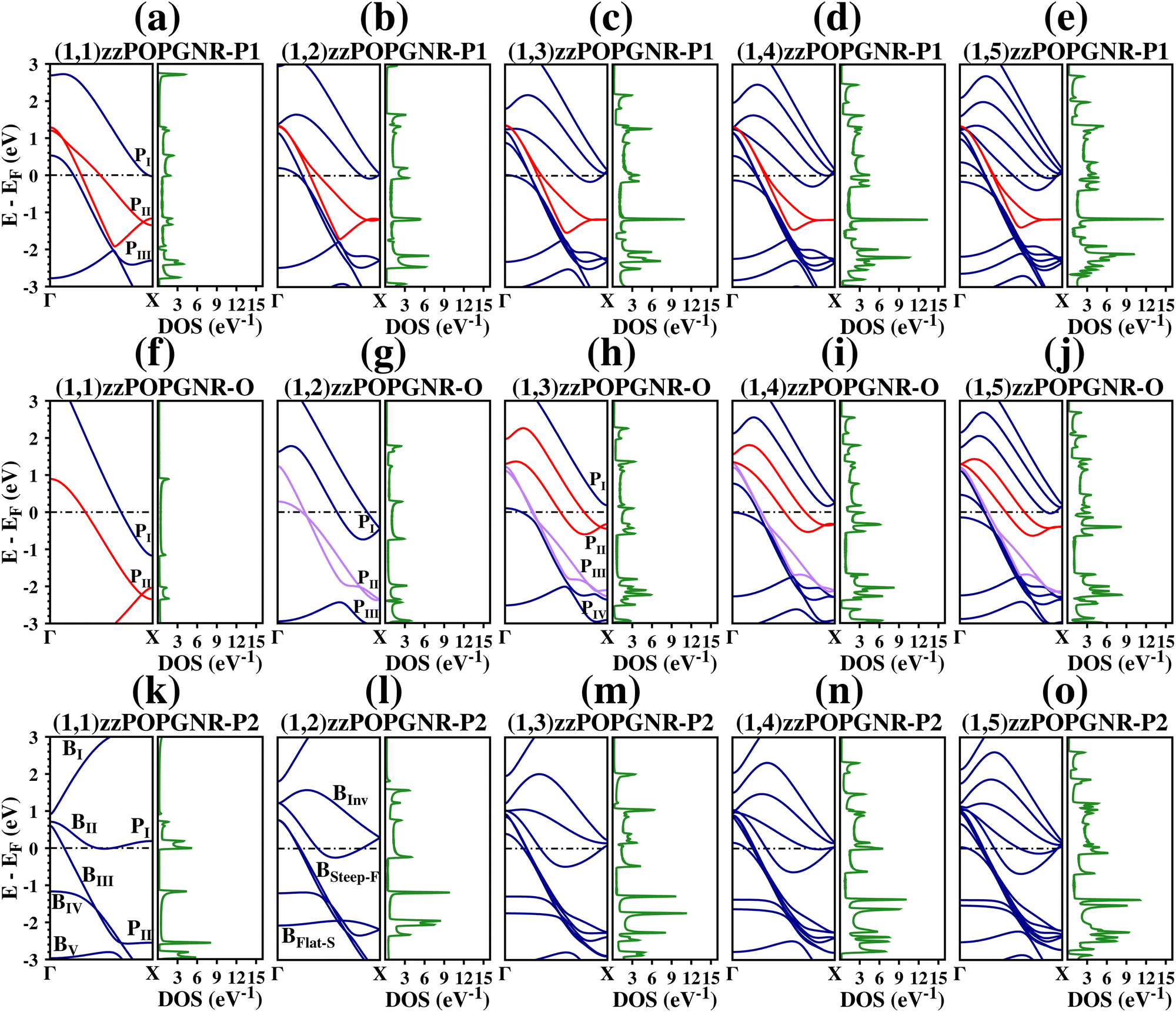 | ||
| Fig. 3 Electronic properties of zigzag POPGNR. From (a)–(e) we have zzPOPGNR-P1, from (f)–(j) zzPOPGNR-O, and from (k)–(o) zzPOPGNR-P2. The horizontal dashed line represents the Fermi level, which was set as zero. | ||
Furthermore, we see that the red-colored bands are Dirac bands in the (1,1)zzPOPGNR-P140,54,55 case, and that these bands become flat and degenerate close to the X-point for the other zzPOPGRN-P1 cases, leading to an intense DOS peak.
The BS and DOS for (1,2)zzPOPGNR-O are shown in Fig. 3(g), where we see that two inter-crossing bands (purple bands) arise, which cross each other at two points (close to the Fermi level and next to the X-point), becoming approximately degenerate after the second crossing point. These bands open the Dirac band presented in Fig. 3(f) and divide the BS into three regions that get to the X-point at three different points in the valence region: approximately at −0.45 eV, −2.40 eV and −3.00 eV, where at the second point (−2.40 eV), the DOS is almost zero.
In Fig. 3(h), for the (1,3)zzPOPGNR-O system, we see that we have two new steep bands: one in the conduction region and one that arises at the Γ-point in the conduction region near the Fermi level, but crosses the Fermi level and intercepts the X-point in the valence region. The new band in the conduction region moves the bands below it and two of these bands become Dirac bands (red bands). The new bands divide the BS into four regions, one above and three below the Fermi level, that get to the X-point at approximately four points: one at approximately 0.20 eV (point I), one around −0.30 eV (point II), one around −2.20 eV (point III) and one around −3.00 eV (point IV) (this pattern remains for the (1,4)zzPOPGNR-O and (1,5)zzPOPGNR-O). The purple bands that emerge in Fig. 3(g) become degenerate in the valence region, from 1.00 eV to −0.40 eV and from −1.90 eV to −2.20 eV.
In Fig. 3(i), we see for (1,4)zzPOPGNR-O that we have three new bands around the Fermi level, two steep bands (one that is in the conduction region (point I)) and another that arises at the Γ-point in the conduction region, but crosses the Fermi level and gets to the X-point in the valence region (point III). There is also a new band in the valence region at the frontier of the interval (point IV). The band in the conduction region (which gets to the X-point at point I) makes the red bands move closer next to the X-point and renders them flat and degenerate, generating a high DOS peak. The band that crosses the Fermi level (which gets to the X-point at point III) generates a double steep band with degeneracy in the valence region from −0.40 eV to −1.00 eV.
For (1,5)zzPOPGNR-O, we see in Fig. 3(j) that we have two new steep bands, one in the conduction region (which gets to the X-point around point I) and one that arises in the conduction region at the Γ-point, crosses the Fermi level, and gets to the X-point in the valence region (around point III). The band in the conduction region moves the bands below it toward the Fermi level, generating a partially-filled band that crosses the Fermi level close to the X-point and squeezes the red bands higher around the X-point, increasing the intensity of the DOS peak at this point. The second new band generates a triple steep band with degeneracy from −0.40 eV to −1.80 eV in the valence region.
In general, we see that zzPOPGNR-P1 (Fig. 3(a)–(e)) has greater conductivity than zzPOPGNR-O (Fig. 3(f)–(j)), since there is an increase in the number of partially-filled bands, i.e., bands that cross the Fermi level from the conduction to the valence region. In the zzPOPGNR-P1 case, the inserted bands in the conduction region move the bands toward the valence regions more than in the zzPOPGNR-O case, and this generates more occupied states. Furthermore, we see that the octa-rings insert steep bands in the conduction and the valence region for both nanoribbons, increasing the nanoribbon conductivity with the width increase.
For (1,1)zzPOPGNR-P2, we see from Fig. 3(k) that we have five bands (BI, BII, BIII, BIV and BV) around the Fermi level (between −3.00 eV and 3.00 eV), and the bands are highly dispersive in the conduction region. We can see that there is a direct sub-bandgap of approximately 0.20 eV in the conduction region between BI and BII at the Γ-point. BII is under the Fermi level between 0.25 and 0.27 (in the k-point range) and is approximately flat after this region, which generates two intense DOS peaks. BIII is flat in the second half of the interval and BIV is approximately flat in the first half, just like BV. These flat aspects generate high DOS peaks at these points.
In Fig. 3(l), we see the BS and DOS for (1,2)zzPOPGNR-P2, and we have two new bands around the Fermi level: one of the BInv kind and one of the BSteep–F kind (which is degenerate with BIII from 0.90 eV to −0.30 eV). Furthermore, we see that BII moves toward the valence region, becoming a partially-filled band, and there is no longer any band on the top of Fermi level. BV moves toward the valence region and we still have a sub-bandgap in the conduction region, but now it is indirect and between BI and the new BInv band. The new sub-bandgap is bigger (0.30 eV) than in the (1,1)zzPOPGNr-P2 case (0.20 eV).
For (1,3)zzPOPGNR-P2 (Fig. 3(m)) we see that there are two new bands: one of the BInv kind and another of the BSteep–F kind. Furthermore, we see that we do not have a sub-bandgap region anymore, because the new BInv band moves the BInv inserted in (1,2)zzPOPGNR-P2 (Fig. 3(l)) toward the conduction direction (far from the Fermi level). The BII band is moved toward the valence region, increasing the region below the Fermi level, which increases its conductivity.
For the (1,4)zzPOPGNR-P2 and (1,5)zzPOPGNR-P2 cases (Fig. 3(n) and (o)), we have the same behavior as for (1,3)zzPOPGNR-P2, with the same new bands and band displacements.
We also can see that, different from the other zz cases in which the bands were steep and less dispersive (Fig. 3(a)–(j)), the bands in the zzPOPGNR-P2 case are in general dispersive, except for the BInv kind, which are dispersive in the conduction region until the middle of the k-point interval, where they start to converge to PI at the X-point.
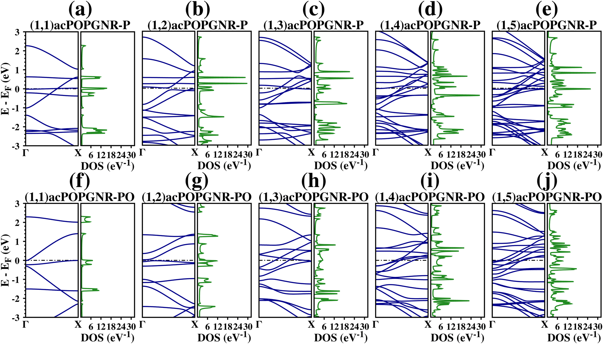 | ||
| Fig. 4 Electronic properties of armchair POPGNR. From (a)–(e) we have acPOPGNR-P, and from (f)–(j) acPOPGNR-PO. The horizontal dashed line represents the Fermi level, which was set to zero. | ||
The BS and DOS of (1,1)acPOPGNR-P are presented in Fig. 4(a); the BS presents nine bands around the Fermi level (−3.00 eV to 3.00 eV), and we have a flat band under Fermi level that results in a high DOS peak. Furthermore, we see that there are three sub-bandgap regions: two above and one below the Fermi level. The first sub-bandgap region is above approximately 2.25 eV; the second is direct and from 0.65 eV to 1.10 eV (gap of 0.45 eV) at the X-point; and the third one is also direct and from −1.00 eV to −1.40 eV (gap of 0.40 eV) at the Γ-point. We see that most of the bands are flat or quasi-flat in this case.
In the (1,2)acPOPGNR-P case (Fig. 4(b)), we see that the nanoribbon has a semiconducting behavior with a very tiny indirect bandgap of 0.053 eV. Furthermore, we see that we have one sub-bandgap region above 2.60 eV, and three flat bands: two above and around the Fermi level and one below it.
In the (1,3)acPOPGNR-P case (Fig. 4(c)), we see that we have four flat bands: one above the Fermi level (at 0.50 eV) and three below it, with two degenerate bands among them (at −0.80 eV), one of which corresponds to a high DOS peak. Furthermore, we see that we have three sub-bandgap regions, two above and one below the Fermi level: one is above 2.60 eV; another is direct and from 0.60 eV to 0.70 eV (gap of 0.10 eV) at the X-point; and the third one is direct and from −1.00 eV to −1.40 eV (gap of 0.40 eV) at the Γ-point.
For (1,4) and (1,5) acPOPGNR-P (Fig. 4(d) and (e)), we see that the bands in the conduction region are dispersive and flat around the Γ-point and converge to small regions at the X-point above Fermi level, crossing each other, while the valence bands emerge from small regions at the Γ-point and are dispersive until they get to the X-point below Fermi level. There are some valence bands that cross the Fermi level in both cases, and some flat bands in the valence region.
We see that there is a direct sub-bandgap region in the (1,5)acPOPGNR-P case, from −1.00 eV to −1.20 eV (bandgap of −0.20 eV) at the Γ-point. Comparing the acPOPGNR-P cases, we see that the sub-bandgap in the valence region only appears for odd numbers of octa-rings ((1,1)acP, (1,3)acP and (1,5)acP cases); for the even ones ((1,2)acP and (1,4)acP), with the width effect, two flat bands arise that converge at approximately −1.40 eV (in the valence sub-bandgap region in the odd cases), which generates a high DOS peak.
For the (1,1)acPOPGNR-PO case, we see from Fig. 4(f) that we have 6 bands between −3.00 eV and 3.00 eV (around the Fermi level), with four sub-bandgap regions: two above the Fermi level (above 2.30 eV and between 1.40 eV and 2.00 eV (direct bandgap of 0.60 eV)) and two below it (between −0.20 eV and −0.30 eV) (direct bandgap of 0.10 eV) and between −2.10 eV and −2.30 eV (direct band-gap of 0.20 eV). Furthermore, we see that we have one flat band at −1.50 eV and two quasi-flat bands (one around 2.20 eV and another in the valence region around Fermi level).
For (1,2)acPOPGNR-PO, we see from Fig. 4(g) that its semiconducting behavior is given by a very tiny bandgap of 0.050 eV. Furthermore, we see that there is a remarkable direct sub-bandgap region above the Fermi level (from 1.60 eV to 2.60 eV (sub-bandgap of 1.00 eV)). We also have two sub-bandgap regions below the Fermi level: one very tiny direct sub-bandgap of 0.048 eV close to the Fermi level and a wide sub-bandgap region of 0.70 eV (from −0.30 eV to −1.00 eV). All these sub-bandgap regions are corroborated by a zero DOS in the corresponding region.
For (1,3)acPOPGNR-PO, we can see from Fig. 4(h) that the bands start to cross each other close to the Fermi level. Most of the bands are dispersive at the Γ-point and converge to a range between −1.20 eV and 0 eV at the X-point. In the valence region, most of the bands are dispersive. Furthermore, we see that there are three sub-bandgap regions, one in the conduction region and two in the valence region: from 2.00 eV to 2.30 eV (indirect sub-bandgap of 0.30 eV), from −0.80 eV to −1.00 eV (indirect sub-bandgap of 0.20 eV) and from −1.80 eV to −2.00 eV (indirect sub-bandgap of 0.20 eV).
For the (1,4)acPOPGNR-PO case (Fig. 4(i)), we observe the disappearance of the sub-bandgap regions in the conduction region. There are only two sub-bandgaps in the valence region, which have lower values relative to those for the previous width: one around −0.70 eV (direct sub-bandgap of approximately 0.050 eV) and another from −1.00 eV to −1.25 eV (indirect sub-bandgap of 0.25 eV).
For the (1,5)acPOPGNR-PO case (Fig. 4(j)), we find the same behavior as for (1,4)acPOPGNR-PO, but with lower sub-bandgap values.
In general, we see for the acPOPGNR-PO case that the sub-bandgap regions are disappear or have drastically lower values with the increase of the nanoribbon width.
3.3 Transport properties
Fig. 5(a), 6(a), 7(a), 8(a) and 9(a) show the nanoribbon molecular devices (for simplicity, we omit the prefix “POPGNR” in the device notation, e.g. (9,1)zzPOPGNR-P1 = (9,1)zzP1). These were designed using the (1,W) (with W from 1 to 4) nanoribbon unit cell as a building block, replicating them nine times for the zz cases (two for the left lead, five for the scattering region, and two for the right lead) and five times for the ac ones (one for the left lead, three for the scattering region, and one for the right lead). Under bias application, we obtained and analyzed the transport properties in terms of electronic current (I) versus bias application (V) (I–V curve), differential conductance (dI/dV) versus V and transmission (T) versus V spectra, and the energy states (E) (T(E,V), where the Fermi level was set as zero) for all the nanodevices.Fig. 5(b) shows the I and dI/dV results for the (9,1)zzP1 case, and we see that the molecular device has an approximately ohmic behavior for lower bias values (from −0.20 V to 0.20 V), with a saturation region in the middle (from ±0.50 V to ±0.70 V), and there is a Negative Differential Resistance (NDR)56,57 region at the end of the interval. Besides a NDR region in the analyzed range, we have a current peak (IPeak) of 87.59 μA at ±0.70 V (VPeak), and a current valley (IValley) of 80.70 μA at ±0.90 V (VValley), with a Peak-to-Valley Current Rate (PVCR) of 1.09.
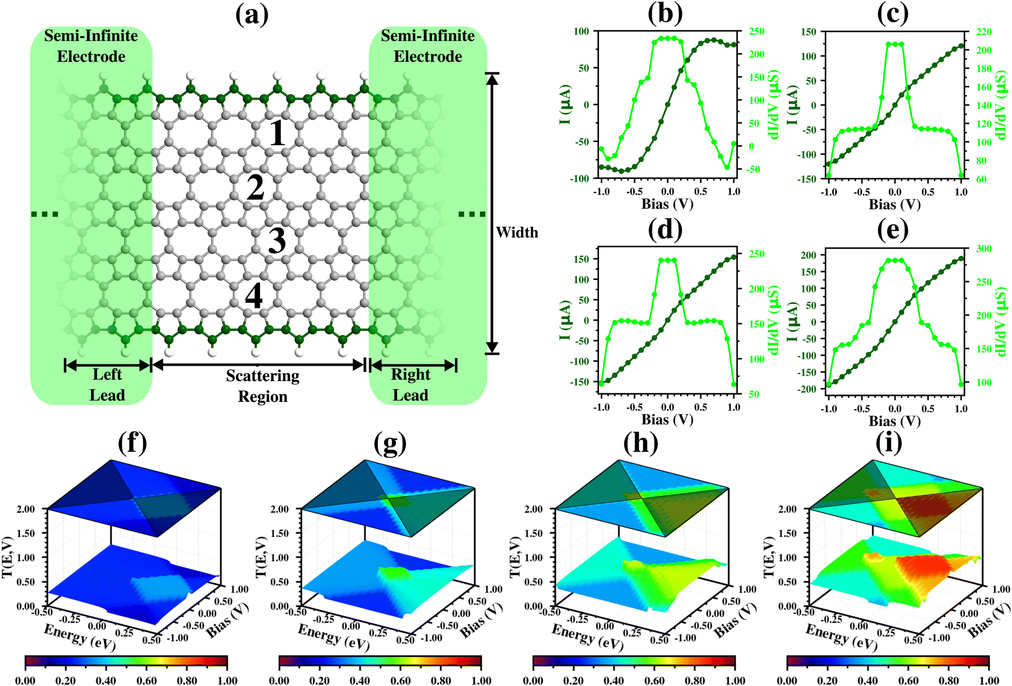 | ||
| Fig. 5 Transport properties of zzPOPGNR-P1. (a) Two-terminal molecular device of zzP1 nanoribbons (width from 1 to 4); (b)–(e) detailed I–V and (dI/dV)–V curves for each molecular device; (f)–(i) transmission spectra of zzP1 molecular devices (width from 1 to 4). The transparent black triangles in (f)–(i) represent the regions outside the bias windows. Only transmission states inside the bias windows contributes to the transport. | ||
These results are corroborated by the dI/dV curve, which shows a horizontal shape for the first region, tends to zero in the second, and has negative values at the end of the interval. Furthermore, both results are corroborated by the analysis of energy states in the T(E,V) graph (Fig. 5(f)), which shows an equal and intense contribution of states with positive and negative energy around 0.00 V, a change in the contribution to be more for positive energy values (light-blue region close to the frontier of the bias window), and a suppression of these states starting from ±0.70 V, explaining the NDR region.
Fig. 5(c) shows the I and dI/dV results for the (9,2)zzP1 case. We see that the molecular device presents two distinct ohmic regions (one between ±0.10 V and another from ±0.30 V to ±0.80 V), and these two regions are divided by a change in the inclination of I (straight line, in these cases). These results are corroborated by the dI/dV curve, which shows horizontal lines in these two regions, and a drastic decrease in the dI/dV division region. Furthermore, we see that both results are corroborated by the analysis of the energy state (T(E,V) graph in Fig. 5(g)), which shows a high transmission in the region between ±0.10 V (green region), and a decrease in the transmission states (light blue region) that becomes constant, with only a small decrease in the contribution at the frontier of the interval.
Fig. 5(d), (e), (h) and (i) show the (9,3)zzP1 and (9,4)zzP1 cases, respectively, and we see that the electronic transport properties (I, dI/dV and T(E,V)) show a similar behavior to the (1,2)zzPOPGNR-P1 case, but with higher values. Furthermore, we see for all zzP1 cases that the main contributions from the energy states in the T(E,V) graph are due to positive energy states, and most of these transmission peak regions are outside the bias windows.
 | ||
| Fig. 6 Transport properties of zzPOPGNR-O. (a) Two-terminal molecular device of zzO nanoribbons (width from 1 to 4); (b)–(e) detailed I–V and (dI/dV)–V curves for each molecular device; (f)–(i) transmission spectra of zzO molecular devices (width from 1 to 4). The transparent black triangles in (f)–(i) represent the regions outside the bias windows. Only transmission states inside the bias window contribute to the transport. | ||
For the (9,1)zzO case, we can see from Fig. 6(b) that the molecular device has an ohmic behaviour over almost all the bias range (from −0.7 V to 0.70 V) and reaches a saturation region from 0.70 V to 1.00 V. These results are corroborated by the dI/dV curve, which shows a horizontal line from −0.7 V to 0.70 V, and a sudden decrease to almost zero, generating the saturation region. These results can also be explained by the transmission spectrum, which shows an equal contribution to the transport by the states with positive and negative values, but a suppression region in the positive energy states emerges starting from 0.70 V, which causes the sudden decrease.
For the cases with W from 2 to 4 (Fig. 6(c)–(e) and (g)–(i)), we see that I has the same behavior as in the (9,1)zzO case (quasi-linear behavior for lower bias values and saturation of I at the end of the investigated interval), but with an increase in values. There are only small differences between the ohmic regions, which become smaller for W = 2 (between ±0.30 V) and W = 3 (between ±0.10 V) and suddenly higher in the (9,4)zzO case. These can be explained by the transmission spectra, which show that in the (9,2)zzO and (9,3)zzO cases the transmission peaks have a major contribution of the negative energy states, in contrast to the (9,4)zzO case, which has a higher and equal contribution of the states with positive and negative energy for the region with ohmic behavior (from −0.7 V to 0.70 V).
These results are in good agreement with the electronic properties, since they show that all the molecular devices have a strong conducting behavior (quasi-linear behavior that happens due to the steep bands crossing the Fermi level), but at the same time, their conductivities are lower than in the zzPOPGNR-P1 case, which has a higher number of the steep bands crossing the Fermi level than the zzPOPGNR-O case.
The Fig. 7(b) shows I for the (9,1)zzP2 case. We can see that I has a quasi-linear shape for lower bias values, and this region can be divided into two, according to the inclination of the I graph (one region between ±0.10 V, and another from ±0.10 V to ±0.50 V). I shows a saturation tendency from ±0.5 V to ±0.7 V, and a decrease from ±0.70 V to ±0.90 V. These results are corroborated by the dI/dV curve, which shows a horizontal line between ±0.10 V and from ±0.10 to ±0.50 V, a sudden decrease from ±0.50 V to ±0.70 V, and a NDR region from ±0.70 V to ±0.90 V. Furthermore, besides a NDR region in the analyzed range, we have IPeak = 22.76 μA at VPeak = ±0.70 V and IValley = 22.36 μA at VValley = ±0.80 V, which give us a PVCR of 1.02. All these results can also be understood using the transmission states, where we can see that the higher conductance between ±0.10 V is given by a transmission peak (blue peak) inside the bias window in this region. The saturation tendency and the NDR region are corroborated by a suppression region (purple region) that arises in the region with negative energy values.
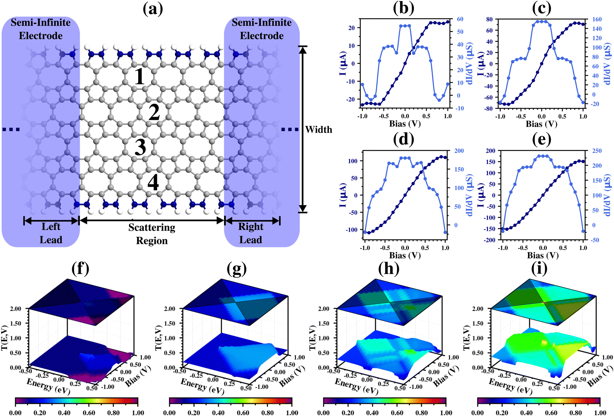 | ||
| Fig. 7 Transport properties of zzPOPGNR-P2. (a) Two-terminal molecular device of zzP2 nanoribbons (width from 1 to 4); (b)–(e) detailed I–V and (dI/dV)–V curves for each molecular device; (f)–(i) transmission spectra of zzP2 molecular devices (width from 1 to 4). The transparent black triangles in (f)–(i) represent the regions outside the bias windows. Only transmission states inside the bias windows contribute to the transport. | ||
The other zzP2 molecular devices with higher widths present transport properties (Fig. 7(c)–(e) and (g)–(i)) with a similar behavior to the (9,1)zzP2 case, but with an increase in the I, dI/dV and T(E,V) values, reduction of the two ohmic regions (starting from the (9,3)zzP2 case, where there is just one), and the displacement of the NDR region, which moves to the end of bias range.
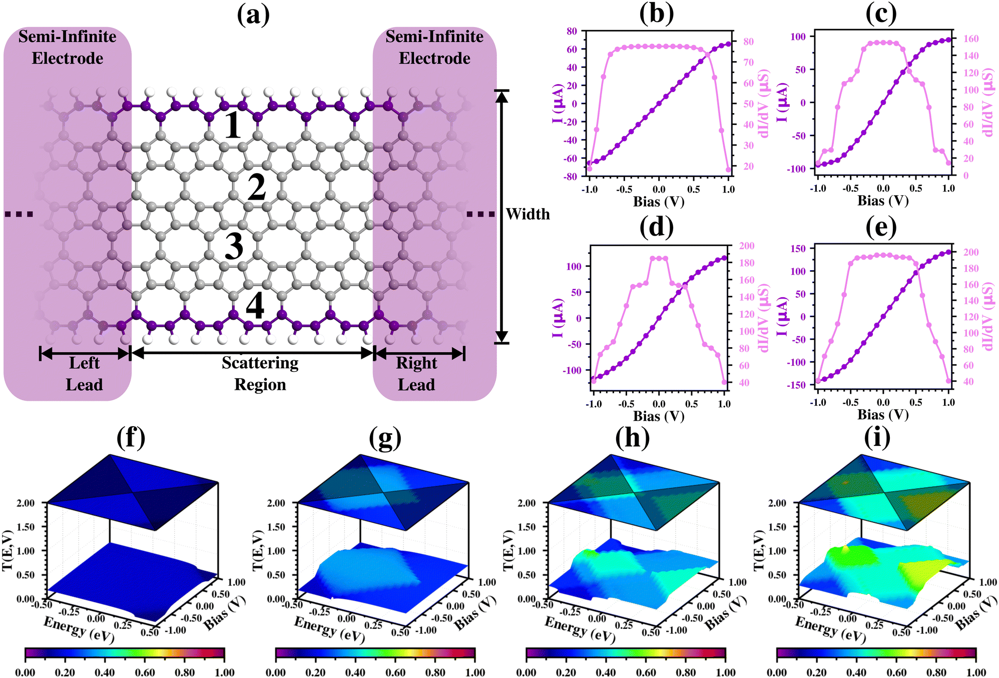
For the (5,1)acP case, we see in Fig. 8(b) that I has an ohmic behaviour between ±0.20 V, shows a very small oscillation from ±0.20 V to ±0.60 V (smoothly increasing and decreasing), reaches a saturation tendency from ±0.60 V to ±0.90 V, and decreases at the end of the interval. This result is corroborated by the dI/dV values, which show a horizontal shape between ±0.20 V, alternation between smoothly increasing and decreasing from ±0.20 V to ±0.60 V, a sudden decrease from ±0.60 V to ±0.90 V, and a NDR region at ±1.00 V. These results are corroborated by the transmission coefficients, which show an equal contribution of the states with positive and negative energy between ±0.20 V (explaining the ohmic behavior), and a decrease in the transmission peaks for high bias values, in a region of negative energy at the frontier of the bias windows (purple region), which explains the sudden decrease and the NDR region.
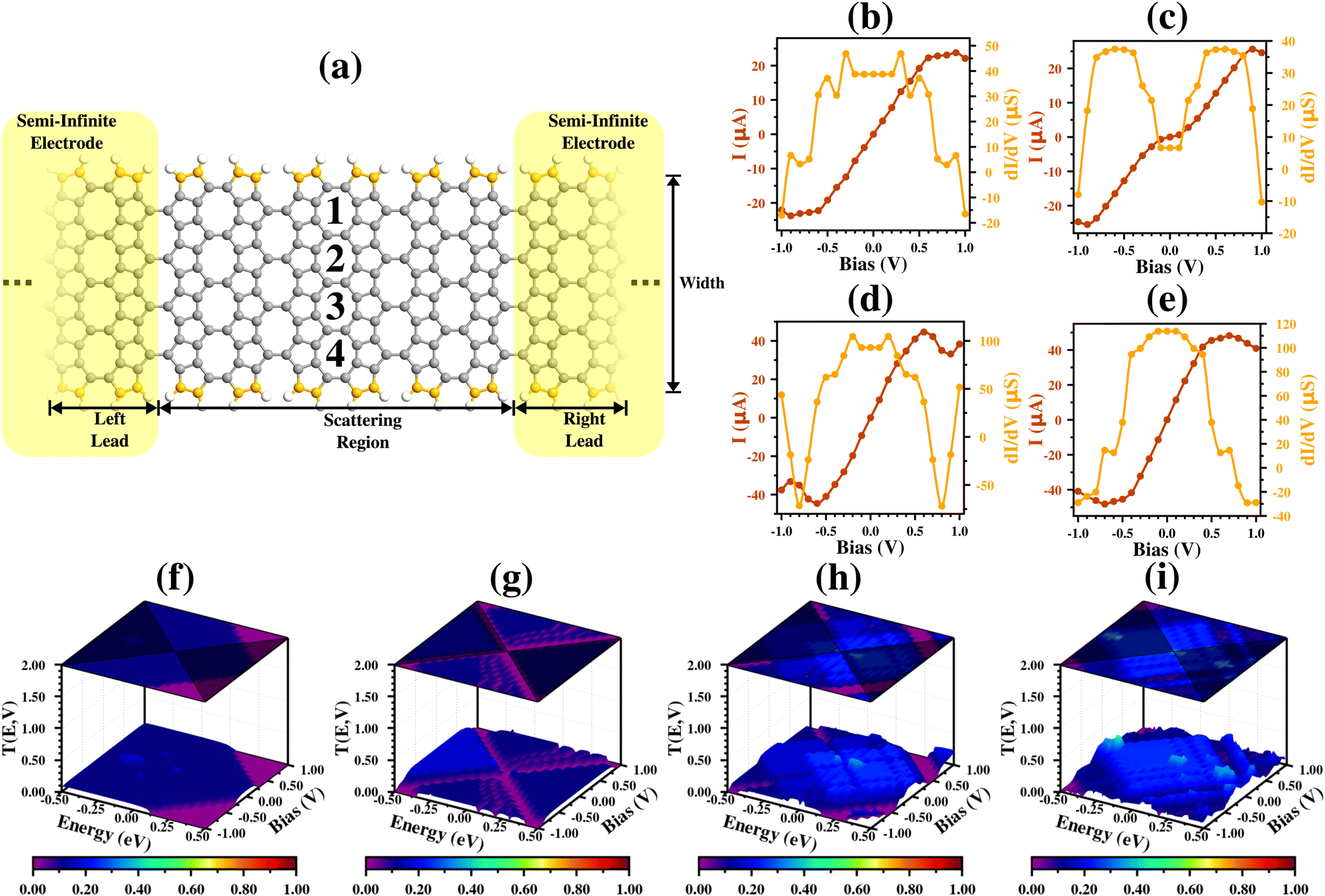 | ||
| Fig. 8 Transport properties of acPOPGNR-P. (a) Two-terminal molecular device of acP nanoribbons (width from 1 to 4); (b)–(e) detailed I–V and (dI/dV)–V curves for each molecular device; (f)–(i) transmission spectra of acP molecular devices (width from 1 to 4). The transparent black triangles in (f)–(i) represent the regions outside the bias windows. Only transmission states inside the bias windows contribute to the transport. | ||
Fig. 8(c) shows the I result for the (5,2)acP molecular device, where we see that for lower bias values, the device shows a slow increase (between ±0.10 V), and then a huge increase (from ±0.10 to ±0.90 V), followed by a decreasing region at the end of the interval (±1.00 V). These results are corroborated by the dI/dV curve, which shows a low and horizontal line between ±0.10 V, a huge increase followed by a horizontal line from ±0.10 V to ±0.90 V, and a NDR region at ±1.00 V. Based on the transmission coefficients, we see that the slow increase is due to almost an absence of transmission states between ±0.10 V, followed by a rise in these starting from ±0.10 V, and the NDR region arises due to an increase in suppression states in the negative energy state region inside the bias windows. The near absence of states for the lower bias values happens due to the tiny bandgap in the (1,2)acPOPGNR structure (Fig. 4(b)).
For the (5,3)acP molecular device (Fig. 8(d)), we see that I has a linear behavior between ±0.50 V, with two different inclinations: one between ±0.10 V and another minor one from ±0.40 V to ±0.50 V. The molecular device reaches a small saturation region from ±0.50 V to ±0.60 V and a decreasing region from ±0.60 V to ±0.90 V, where it then starts to increase again. These results are corroborated by the dI/dV values, which show a horizontal line between ±0.10 V, a sudden decrease from ±0.50 V to ±0.60 V, and a NDR region from ±0.70 V to ±0.90 V, with an inversion point at ±0.90 V. Furthermore, besides a NDR region in the analyzed range, we have IPeak = 44.58 μA at VPeak = ±0.60 V and IValley = 33.16 μA at VValley = ±0.90 V, which give us a PVCR of 1.34. These results can also be understood via the transmission spectrum (Fig. 8(h)), which shows the emergence of a suppression state region (purple region) from ±0.70 V to ±0.90 V for both energy states (generating the NDR region), and the emergence of state transmission at the frontier of the bias windows, with negative energy values, which results in the inversion point and increases in I. Furthermore, we see that the (5,4)acP molecular device (Fig. 8(e) and (i)) has a similar behavior to that of (5,3)acP, but with a saturation region from ±0.40 V to ±0.70 V, and a NDR from ±0.70 V to ±1.00 V, with the disappearance of the inversion point.
We see that the I values are much lower than in the zz case. These results can be understood via the BS/DOS results, which show flat bands for this kind of molecular device system, against steep bands more deeply crossing the Fermi level for the zz ones.
The results for the (5,1)acPO molecular device are presented in Fig. 9(b) and (f). We see from Fig. 9(b) that I shows a linear behavior between ±0.10 V, a saturation region from ±0.10 V to ±0.30 V, and then an approximately exponential increase starting from ±0.30 V. These results are corroborated by the dI/dV values, which show a horizontal shape between ±0.10 V, a decrease followed by a stabilization from ±0.10 V to ±0.30 V, and an intense increase starting from ±0.30 V. Furthermore, besides a NDR region in the analyzed range, we have IPeak = 1.23 μA at VPeak = ±0.10 V and IValley = 0.76 μA at VValley = ±0.30 V, which give us a PVCR of 1.61. These results are in agreement with the transmission states, since we see that the increase after ±0.30 V happens due to the emergence of a region with high transmission (relative to this nanodevice) in the positive energy states.
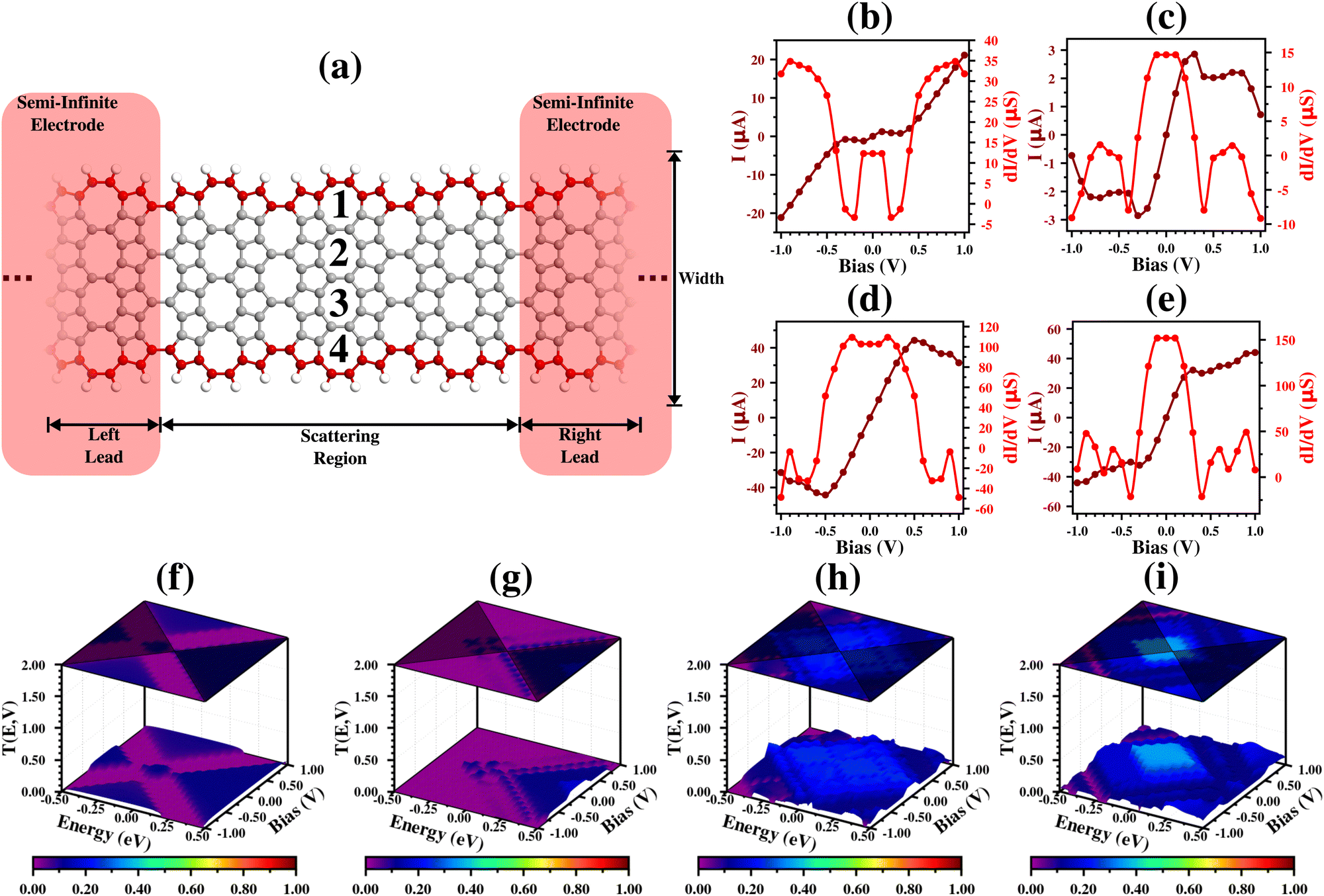 | ||
| Fig. 9 Transport properties of acPOPGNR-PO. (a) Two-terminal molecular device of acPO nanoribbons (width from 1 to 4); (b)–(e) detailed I–V and (dI/dV)–V curves for each molecular device; (f)–(i) transmission spectra of acPO molecular devices (width from 1 to 4). The transparent black triangles in (f)–(i) represent the regions outside the bias windows. Only transmission states inside the bias windows contribute to the transport. | ||
Fig. 9(c) and (g) show the results for the (5,2)acPO molecular device, where we can see that I has the lowest values among those of all investigated molecular devices in this work. Furthermore, we see that I has a linear behavior between ±0.20 V, two saturation regions from ±0.20 V to ±0.30 V and from ±0.40 V to ±0.80 V (separated by a fall between ±0.30 V and ±0.40 V), and a decrease starting from ±0.80 V. The results are in agreement with the dI/dV curve, which shows a horizontal shape between ±0.10 V and a sudden decrease from ±0.10 V to ±0.40 V, with a NDR at ±0.40 V, an increase with a quasi-horizontal shape from ±0.50 V to ±0.70 V, and another NDR region starting from ±0.80 V. Furthermore, besides a NDR region in the analyzed range, we have IPeak = 2.86 μA at VPeak = ±0.30 V and IValley = 2.02 μA at VValley = ±0.50 V, which give us a PVCR of 1.41. These results can also be explained via the transmission spectrum, which shows a very low value for all almost all the bias window, except for a line of peaks (blue points) that starts in the positive/negative division region between ±0.20 V, and proceeds only in the negative energy region.
For the (5,3)acPO and (5,4)acPO cases, we see a similar behavior to the (5,2)acPO ones, but with reduction of the saturation regions (Fig. 9(d) for (5,3)acPO) and most of the NDR regions for high bias values (Fig. 9(e) for (5,4)acPO). For the (5,4)acPO case, besides a NDR region in the analyzed range, we have IPeak = 32.17 μA at VPeak = ±0.30 V and IValley = 30.04 μA at VValley = ±0.40 V, which give us a PVCR of 1.07.
4 Conclusions
In this work, we conducted a first-principles investigation of the effect of width on the features of five carbon nanoribbons (three zz: zzP1, zzO and zzP2; and two ac: acP and acPO) with 5-8-5 carbon ring symmetry based on a 2D carbon allotrope named POPG. We analyzed the stability using cohesive energy results and structural results (in comparison with the literature in this area), the electronic properties (via BS and DOS), and the transport properties and possible molecular device applications using I, dI/dV and T(E,V) results.The cohesive energy results and structural parameters show that all the investigated nanoribbons are stable and feasible for being experimentally obtained, since the cohesive energy results are negative, and are in the range of those of several predicted carbon allotropes (some already experimentally obtained), and the bond lengths are in good agreement with those of carbon allotropes in the literature. Furthermore, carbon ribbons with 5- and 8-carbon ring symmetry have already been experimentally obtained.34–36 Furthermore, the cohesive energy results show that the penta-rings have a major role in nanoribbon stability with the variation of the width (a generalization of the results presented in ref. 41), since the nanoribbons with this edge termination have the lowest Ecoh values, and the zzP1 cases have the lowest Ecoh variation (ΔEcoh = 0.51 eV/atom). Furthermore, the structural results suggest that most of the nanoribbons experience a uniaxial tensile strain application due to the edge shape and width effect, but the width effect has a major role in this phenomenon, since this uniaxial tensile strain effect increases with the decrease of the nanoribbon width (quantum confinement effect).
The transport results for the zzP1 case show that this kind of nanoribbon has a strong metallic behavior, since in general we have an ohmic and quasi-linear behavior in the analyzed interval. The exception is for the (1,1)zzP1 case, which has a tendency for a saturation region from ±0.50 V to ±0.70 V and a NDR from ±0.70 V to ±0.90 V. These results indicate hybrid molecular device behavior, which suggests applications that resemble a FET in the range of −0.70 V to 0.70 V and a RTD from ±0.70 V to ±1.00 V. These behaviors are lost with the increase of the width ((1,2)zzP1 case or higher).
For the zzO cases, the transport properties show that in general, the molecular devices have a quasi-linear ohmic behaviour for lower/medium bias voltage values, and have a saturation tendency at the end of the analyzed interval. These results suggests that all these kinds of molecular devices have a behavior that resembles a FET molecular device from −1.00 V to 1.00 V. Furthermore, a similar behavior is observed for the zzP2 devices, but with the rise of NDR regions at the end of the bias range. Therefore a hybrid FET and RTD behavior is presented in molecular devices based on this kind of structure.
For the acP and acPO cases, we see that the molecular devices have several hybrid device behaviors, with a strong dependence on the nanoribbon width. The (5,1)acPO device has a hybrid behavior of a FET between ±0.20 V, a RTD at ±0.30 V (due to the NDR region), and a Zener Diode (ZD) starting at bias higher than ±0.30 V. The same behavior is presented in (5,1)acPO, but for a different bias range. For the other acP and acPO cases, we have a hybrid behavior of FET and RTD in different operation ranges.
Since in all the investigated cases most of the transmission peaks are outside the bias windows, the use of a third terminal (a gate, for instance) could be useful to shift them inside the bias windows, which could improve the device operation.
Therefore, the results show that the zz molecular devices have, in general, the behavior of a FET or RTD, and the armchair ones have more interesting features, with FET, RTD and ZD behavior, besides several sub-bandgap regions that can possibly suggest applications as optoelectronic devices. Since these kinds of nanoribbons have a large range of device behaviors tuned by the width effect, these materials arise as an excellent alternative for applications in nanoelectronics.
Author contributions
Elder Augusto Viana Mota: investigation, methodology, formal analysis, visualization, writing – original draft, writing – review & editing. Carlos Alberto Brito da Silva Jr: funding acquisition, writing – review & editing. Jordan Del Nero: funding acquisition, supervision.Conflicts of interest
There are no conflicts to declare.Acknowledgements
The author E. A. V. M. is very grateful to the Brazilian agency CAPES for financial support [grant number 1776696]. C. A. B. da S. Jr is very grateful to the Brazilian agency PROPESP/PIBIC/UFPA for financial support [grant number PRO4697-2020]. J. D. N. is very grateful to the Brazilian agency CNPq for financial support [grant number 306266/2017-2].Notes and references
- J. E. Field, Rep. Prog. Phys., 2012, 75, 126505 CrossRef CAS PubMed.
- V. Rimal and P. K. Srivastava, IOP Conf. Ser.: Mater. Sci. Eng., 2022, 1219, 012018 Search PubMed.
- Y. Zhang, Y. W. Tan, H. L. Stormer and P. Kim, Nature, 2005, 438, 201–204 CrossRef CAS PubMed.
- P. Gehring, A. Harzheim, J. Spièce, Y. Sheng, G. Rogers, C. Evangeli, A. Mishra, B. J. Robinson, K. Porfyrakis, J. H. Warner, O. V. Kolosov, G. A. D. Briggs and J. A. Mol, Nano Lett., 2017, 17, 7055–7061 CrossRef CAS.
- K. S. Novoselov, A. K. Geim, S. V. Morozov, D. Jiang, Y. Zhang, S. V. Dubonos, I. V. Grigorieva and A. A. Firsov, Science, 2004, 306, 666–669 CrossRef CAS.
- A. R. Urade, I. Lahiri and K. Suresh, JOM, 2023, 75, 614–630 CrossRef CAS PubMed.
- E. Pollak, B. Geng, K.-J. Jeon, I. T. Lucas, T. J. Richardson, F. Wang and R. Kostecki, Nano Lett., 2010, 10, 3386–3388 CrossRef CAS PubMed.
- E. Lee and K. A. Persson, Nano Lett., 2012, 12, 4624–4628 CrossRef CAS.
- F. Schwierz, Nat. Nanotechnol., 2010, 5, 487–496 CrossRef CAS.
- S. Roche, Nat. Nanotechnol., 2011, 6, 8–9 CrossRef CAS.
- C. Su, H. Jiang and J. Feng, Phys. Rev. B: Condens. Matter Mater. Phys., 2013, 87, 075453 CrossRef.
- L. Vicarelli, S. J. Heerema, C. Dekker and H. W. Zandbergen, ACS Nano, 2015, 9, 3428–3435 CrossRef CAS.
- Z. Wang, X.-F. Zhou, X. Zhang, Q. Zhu, H. Dong, M. Zhao and A. R. Oganov, Nano Lett., 2015, 15, 6182–6186 CrossRef CAS PubMed.
- F. M. de Vasconcelos, A. G. S. Filho, E. C. Girão and V. Meunier, Carbon, 2020, 167, 403–413 CrossRef.
- Y. Luo, C. Ren, Y. Xu, J. Yu, S. Wang and M. Sun, Sci. Rep., 2021, 11, 19008 CrossRef CAS PubMed.
- X. Fan, J. Li and G. Chen, RSC Adv., 2017, 7, 17417–17426 RSC.
- S. Thomas, C. H. Lee, S. Jana, B. Jun and S. U. Lee, J. Phys. Chem. C, 2019, 123, 21345–21352 CrossRef CAS.
- S. Wang, Y. Si, B. Yang, E. Ruckenstein and H. Chen, J. Phys. Chem. Lett., 2019, 10, 3269–3275 CrossRef CAS.
- Y. Du, J. Maassen, W. Wu, Z. Luo, X. Xu and P. D. Ye, Nano Lett., 2016, 16, 6701–6708 CrossRef CAS.
- J.-W. Jiang, T. Chang, X. Guo and H. S. Park, Nano Lett., 2016, 16, 5286–5290 CrossRef CAS PubMed.
- Y. Gu, Z. Qiu and K. Müllen, J. Am. Chem. Soc., 2022, 144, 11499–11524 CrossRef CAS.
- T. A. Oliveira, P. V. Silva and E. C. Girão, Phys. Chem. Chem. Phys., 2022, 24, 26813–26827 RSC.
- Z. Zhu, Z. G. Fthenakis and D. Tománek, 2D Mater., 2015, 2, 035001 CrossRef.
- C. Xu, P. Ning, C. Luo, L. Cao, X. Deng and G. Zhou, Phys. E, 2022, 136, 115003 CrossRef CAS.
- C. Luo, T. Chen, X. Dong, L. Xie, D. Qin, L. Huang, H. Lic and X. Xiao, J. Mater. Chem. C, 2023, 11, 9114–9123 RSC.
- F. M. de Vasconcelos, A. G. S. Filho, V. Meunier and E. C. Girão, Phys. Rev. Mater., 2019, 3, 066002 CrossRef.
- H. Terrones, R. Lv, M. Terrones and M. S. Dresselhaus, Rep. Prog. Phys., 2012, 75, 062501 CrossRef.
- N. Rosenkranz, M. Mohr and C. Thomsen, Ann. Phys., 2011, 523, 137–144 CrossRef CAS.
- C. J. Dai, X. H. Yan, Y. Xiao and Y. D. Guo, EPL, 2014, 107, 37004 CrossRef.
- Y. Liu, G. Wang, Q. Huang, L. Guo and X. Chen, Phys. Rev. Lett., 2012, 108, 225505 CrossRef.
- P. Yuan, Z. Fan and Z. H. Zhang, Carbon, 2017, 124, 228–237 CrossRef CAS.
- B. Rajbanshi, S. Sarkar, B. Mandal and P. Sarkar, Carbon, 2016, 100, 118–125 CrossRef CAS.
- S. Zhang, J. Zhou, Q. Wang, X. Chen, Y. Kawazoe and P. Jena, Proc. Natl. Acad. Sci. U. S. A., 2015, 112, 2372–2377 CrossRef CAS PubMed.
- J. Lahiri, Y. Lin, P. Bozkurt, I. I. Oleynik and M. Batzill, Nat. Nanotechnol., 2010, 5, 326–329 CrossRef CAS PubMed.
- J. Kotakoski, A. V. Krasheninnikov, U. Kaiser and J. C. Meyer, Phys. Rev. Lett., 2011, 106, 105505 CrossRef CAS PubMed.
- J. H. Chen, G. Autés, N. Alem, F. Gargiulo, A. Gautam, M. Linck, C. Kisielowski, O. V. Yazyev, S. G. Louie and A. Zettl, Phys. Rev. B: Condens. Matter Mater. Phys., 2014, 89, 121407 CrossRef.
- S. Wang, B. Yang, H. Chen and E. Ruckenstein, J. Mater. Chem. A, 2018, 6, 6815–6821 RSC.
- W. H. S. Brandão, A. L. Aguiar, L. A. Ribeiro, D. S. Galvão and J. M. D. Sousa, ChemPhysChem, 2021, 22, 701–707 CrossRef.
- M. L. P. Júnior, L. A. R. Júnior, W. H. S. Brandão, A. L. Aguiar, D. S. Galvão and J. M. de Sousa, ChemPhysChem, 2020, 21, 1918–1926 CrossRef.
- E. A. V. Mota, M. Moura-Moreira, M. R. S. Siqueira, C. A. B. da Silva Jr and J. D. Nero, Phys. Chem. Chem. Phys., 2021, 23, 2483–2490 RSC.
- E. A. V. Mota, C. A. B. da Silva Jr and J. D. Nero, Phys. Chem. Chem. Phys., 2022, 24, 29966–29976 RSC.
- A. León, W. Orellana, E. S. Morell and M. Pacheco, Phys. Rev. B, 2020, 101, 085408 CrossRef.
- O. V. Yazyev, Acc. Chem. Res., 2013, 46, 2319–2328 CrossRef CAS PubMed.
- K. Bang, S. Chee, K. Kim, M. Son, H. Jang, B. H. Lee, K. H. Baik, J. Myoung and M. Ham, Nano Convergence, 2018, 5, 7 CrossRef.
- P. Hohenberg and W. Kohn, Phys. Rev., 1964, 136, B864–B871 CrossRef.
- W. Kohn and L. J. Sham, Phys. Rev., 1965, 140, A1133–A1138 CrossRef.
- E. A. V. Mota, M. V. da, S. Paula, C. A. B. da Silva Jr and J. D. Nero, Mater. Lett., 2023, 336, 133925 CrossRef CAS.
- J. M. Soler, E. Artacho, J. D. Gale, A. García, J. Junquera, P. Ordejón and D. Sánchez-Portal, J. Phys.: Condens. Matter, 2002, 14, 2745–2779 CrossRef CAS.
- J. P. Perdew, K. Burke and M. Ernzerhof, Phys. Rev. Lett., 1996, 77, 3865–3868 CrossRef CAS PubMed.
- M. Brandbyge, J.-L. Mozos, P. Ordejón, J. Taylor and K. Stokbro, Phys. Rev. B: Condens. Matter Mater. Phys., 2002, 65, 165401 CrossRef.
- N. Papior, N. Lorente, T. Frederiksen, A. García and M. Brandbyge, Comput. Phys. Commun., 2017, 212, 8–24 CrossRef CAS.
- D. Ferreira, W. Oliveira, M. Siqueira, C. Silva and J. D. Nero, Mater. Lett., 2023, 347, 134609 CrossRef CAS.
- M. Büttiker, Y. Imry, R. Landauer and S. Pinhas, Phys. Rev. B: Condens. Matter Mater. Phys., 1985, 31, 6207–6215 CrossRef.
- C. Zhong, Y. Xie, Y. Chen and S. Zhang, Carbon, 2016, 99, 65–70 CrossRef CAS.
- A. K. Geim and K. Novoselov, Nat. Mater., 2007, 6, 183–191 CrossRef CAS.
- A. Pramanik, S. Sarkar and P. Sarkar, J. Phys. Chem. C, 2012, 116, 18064–18069 CrossRef CAS.
- B. Mandal, S. Sarkar, A. Pramanika and P. Sarkar, Phys. Chem. Chem. Phys., 2013, 15, 21001–21006 RSC.
Footnote |
| † Electronic supplementary information (ESI) available. See DOI: https://doi.org/10.1039/d3tc03701k |
| This journal is © The Royal Society of Chemistry 2024 |