
Robust large area molecular junctions based on transparent and flexible electrodes†
Aitor
García-Serrano
ab,
Pilar
Cea
 *abc,
Henrry M.
Osorio
d,
Francesc
Pérez-Murano
e,
Gemma
Rius
e,
Paul J.
Low
f and
Santiago
Martin
*abc
*abc,
Henrry M.
Osorio
d,
Francesc
Pérez-Murano
e,
Gemma
Rius
e,
Paul J.
Low
f and
Santiago
Martin
*abc
aInstituto de Nanociencia y Materiales de Aragón (INMA), CSIC-Universidad de Zaragoza, 50009 Zaragoza, Spain. E-mail: pilarcea@unizar.es; smartins@unizar.es
bDepartamento de Química Física, Facultad de Ciencias, Universidad de Zaragoza, 50009, Zaragoza, Spain
cLaboratorio de Microscopias Avanzadas (LMA) Campus Río Ebro, Universidad de Zaragoza, C/Mariano Esquilor, s/n, 50018 Zaragoza, Spain
dDepartamento de Física, Escuela Politécnica Nacional, Av. Ladrón de Guevara, E11-253, 170525 Quito, Ecuador
eInstituto de Microelectrónica de Barcelona (IMB-CNM, CSIC), Campus UAB, 08193 Bellaterra, Spain
fSchool of Molecular Sciences, University of Western Australia, 35 Stirling Highway, Crawley, Perth, 6009, Australia
First published on 7th December 2023
Abstract
Electrografting of an oligophenylene ethynylene monolayer (OPEH) onto a Mylar®-supported PEDOT![[thin space (1/6-em)]](https://www.rsc.org/images/entities/char_2009.gif) :PSS and graphene substrate prior to wet-transfer of a graphene top-electrode has been used to create flexible and transparent large-area Mylar–PEDOT:PSS|OPEH|Graphene molecular junctions. The electrical conductance of the Mylar–PEDOT:PSS|OPEH|Graphene structure was determined by conductive probe atomic force microscopy (c-AFM), sampling various regions across the surfaces of multiple devices. All registered I–V curves (sampling size ∼150 tests) give a sigmoidal response, consistent with through molecule conductance and ruling out the presence of direct electrode contacts or short-circuits. The demonstration of the combined use of Mylar-supported PEDOT:PSS and graphene as alternative electrode materials to conventional metal thin film electrodes in large-area molecular junctions opens avenues to enable flexible and transparent molecular (opto)electronic devices.
:PSS and graphene substrate prior to wet-transfer of a graphene top-electrode has been used to create flexible and transparent large-area Mylar–PEDOT:PSS|OPEH|Graphene molecular junctions. The electrical conductance of the Mylar–PEDOT:PSS|OPEH|Graphene structure was determined by conductive probe atomic force microscopy (c-AFM), sampling various regions across the surfaces of multiple devices. All registered I–V curves (sampling size ∼150 tests) give a sigmoidal response, consistent with through molecule conductance and ruling out the presence of direct electrode contacts or short-circuits. The demonstration of the combined use of Mylar-supported PEDOT:PSS and graphene as alternative electrode materials to conventional metal thin film electrodes in large-area molecular junctions opens avenues to enable flexible and transparent molecular (opto)electronic devices.
Introduction
Molecular electronics is the term used to describe a broad field of endeavour in which single molecules, bundles of a few molecules, or many molecules in monolayer assemblies are used to modulate the transmission of charge between two macroscopic electrodes. Although single-molecule electrode|molecule|electrode junctions have proven to be remarkably versatile research tools,1–9 and led to many proposals for applications beyond mimicry of conventional electronic components,10 the translation of molecular electronic science to a practical molecular electronic technology arguably requires junctions in which monolayer assemblies are reliably contacted between larger-area electrodes to better enable integration with existing technologies and interface with the macroscopic world.11–16 The fabrication of these large-area devices typically involves the deposition of a molecular high-quality monolayer by self-assembly,17–20 Langmuir–Blodgett,21–25 electrografting,26–30etc. onto a bottom electrode, usually formed from a conductive material deposited onto a rigid substrate and subsequent deposition of a top electrode. The top electrode must be deposited uniformly or patterned over the surface in such a way as to ensure good electrical contact with the monolayer, without damaging, penetrating, or altering the molecular monolayer or contaminating the surface interface, and using readily scaled methods.11,31–35 However, despite immense efforts to develop top contact electrodes from various conducting polymers,16 graphene,36–38 transparent e-carbon layers,39 carbon-FEBID films,40 eGaIn,41–43 or thin layers of metals,11,34,44–50 the intrinsic rigidity of the supporting substrates restrict the use of molecular electronic technologies in the fabrication of transparent, flexible and stretchable devices, with a rather limited number of papers reporting molecular junctions having some of these properties.51–53In this regard, conductive polymers are interesting substrate materials that have proven of use in portable and flexible organic semi-conductor electronics owing to their favourable mechanical properties and electrical tunability. With a view to a cross-over technology that draws upon the advantages of flexible organic semiconductor electronics to advance molecular junction based platforms, the mixture of ionomers poly(3,4-ethylenedioxythiophene):poly(styrenesulfonate) (PEDOT:PSS) can be identified as a material for building flexible substrate electrodes due to the high electrical conductivity and optical transparency, coupled with environmental stability, flexibility, tuneable mechanical stiffness and biocompatibility.54–59
We report here the fabrication of large area molecular junctions based on a Mylar-supported PEDOT:PSS bottom electrode, modified by a wire-like oligo (phenylene ethynylene) molecular monolayer, via the well-known procedures of in situ chemical resuction of an aniline-terminal group to a diazonium salt and subsequent electrografting pioneered by McCreery for the fabrication of carbon-based molecular junctions.60–62 The resulting PEDOT:PSS|OPE monolayer was subsequently covered with a graphene top electrode.63–66 The resulting devices are shown to offer consistent electrical properties, reliable formation with high device yield, whilst retaining outstanding optical transparency across the visible spectrum.
Experimental section
Materials and reagents
The compound 4-(4-(4-(trimethylsilylethynyl)phenylethynyl)phenylethynyl) aniline (1), was synthesized as previously reported.67 Anhydrous acetonitrile (ACN), dimethyl sulfoxide (DMSO) and methanol (MeOH) were purchased from Sigma-Aldrich whilst isopropyl alcohol (IPA) was acquired from Fischer. Tetraethylammonium tetrafluoroborate (≥99.0% from Sigma-Aldrich), NEt4BF4, was dried at 80 °C in vacuum for 24 h before use. The compounds tert-butylnitrite (tBuONO, 90% from Sigma-Aldrich), potassium chloride (KCl, 99% from Fluka), potassium carbonate (K2CO3, 99% from Labbox) and potassium ferrocyanide (K4[Fe(CN)6], ≥99% from Scharlau) were used as received. An aqueous dispersion of (3,4-ethylenedioxythiophene) polystyrene sulfonate (PEDOT:PSS 1:1.3, CleviosTM PH1000) was purchased from HERAEUS PHX. Anhydrous ethylene glycol (EG) and (3-glycidyloxypropyl)trimethoxysilane (GOPS) and polyethylene terephthalate (Mylar®) were acquired from Sigma-Aldrich.
Generation of the diazonium salt
An acetonitrile solution of compound 1 (2.5 mM), tert-butyl nitrite (7.5 mM) and NEt4BF4 (0.1 M) was stirred for 30 min in an electrochemical cell under an inert nitrogen atmosphere to promote formation of the diazonium salt, which was used as formed in situ.Characterization techniques
The spin-coated films were processed using a Delta20T2/200 spin coater by Suss MicroTec. Electrochemical measurements were performed using an Autolab PGSTAT302N potentiostat (Metrohm-Autolab, BV, the Netherlands), with a Pt sheet counter electrode. For the electrografting experiments in acetonitrile, a non-aqueous Ag/Ag+ (0.01 M AgNO3 in acetonitrile) reference electrode, purchased from BAS, was employed and calibrated against the ferrocene/ferricenium couple (E(Fc/Fc+) = 90 mV). For aqueous electrochemical work, a Ag/AgCl//3 M KCl reference electrode from Metrohm was used. All potentials in the text are reported against the appropriate reference electrode for the solvent employed. Atomic force microscopy (AFM) images were obtained using a Bruker Multimode 8 microscope, equipped with a Nanoscope V control unit and RFESPA-75 (75–100 kHz, and 1.5–6 N m−1, nominal radius of 8 nm) tips, in tapping mode. The microscope was operated under ambient conditions in air using a scan rate of 0.5–1.2 Hz. Determination of the RMS roughness and depth statistical analysis were carried out by means of Nanoscope off-line v. 1.40 and Gwyddion v. 2.41 package softwares. X-ray photoelectron spectroscopy (XPS) spectra were recorded using a Kratos AXIS ultra DLD spectrometer with a monochromatic Al Kα X-ray source (1486.6 eV) employing a pass energy of 20 eV. The XPS binding energies were all referenced to the C1s peak at 284.6 eV. Raman spectra were collected using a confocal Raman imaging from Witec, model Alpha300M+ with an excitation wavelength of 633 nm.Molecular conductance measurements
A Bruker ICON microscope in the peak force tunneling AFM (PF-TUNA™) mode with a PF-Tapping™ cantilever tip from Bruker (coated with Pt/Ir 20 nm, ca. 25 nm radius, 0.4 N m−1 spring constant and 70 kHz resonance frequency) was used to perform the conductive-AFM (c-AFM) measurements under conditions of closely controlled humidity (ca. 30%), in an N2 atmosphere.Results and discussion
The general principles of the flexible large-area junction assembly process are summarised in Scheme 1. A PEDOT:PSS solution was deposited by spin coating onto a Mylar® support and over this PEDOT:PSS film, a trimethylsilyl-protected ethynyl-functionalized oligo(phenylene ethynylene) monolayer was electrografted from a diazonium salt synthesized in situ from the amine-functionalised analogue (1) (Scheme 1). The bulky trimethylsilyl (TMS) group serves to protect the assembling monolayer from dendritic growth during the electrografting step, and affords a well-formed covalently bonded monolayer on the Mylar–PEDOT:PSS electrode. To complete the junction, the trimethylsilyl group was removed to expose the terminal alkyne moiety and a graphene layer was deposited over the organic monolayer using a wet transfer process (Scheme 1).
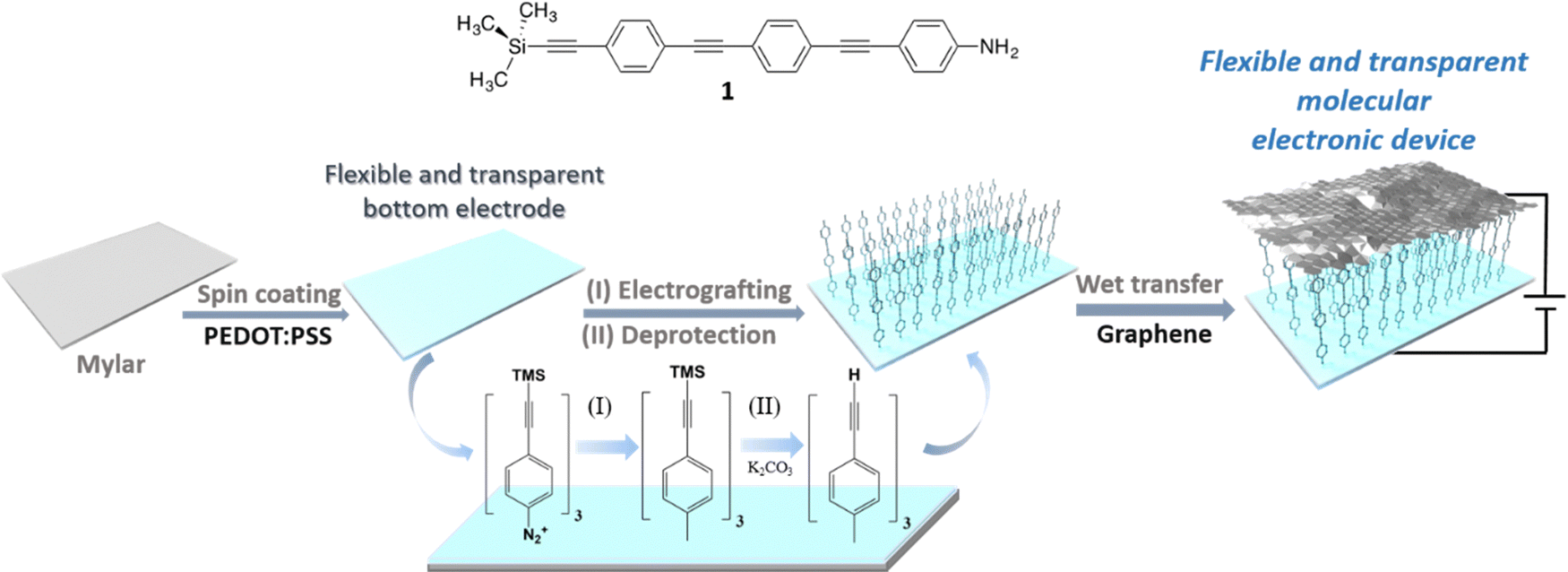 | ||
| Scheme 1 Chemical structure of molecular compound used in this work, 4-(4-(4-(trimethylsilylethynyl)phenylethynyl)phenylethynyl) aniline (1), and a cartoon illustrating the processing sequence used to fabricate the robust large area molecular junctions based on transparent and flexible electrode materials. | ||
Fabrication of the Mylar–PEDOT![[thin space (1/6-em)]](https://www.rsc.org/images/entities/h3_char_2009.gif) :PSS substrate
:PSS substrate
Polyethylene terephthalate (Mylar®) film was selected as the support material for the construction of the bottom electrode in the large-area junction devices, offering the key features of flexibility, transparency, and low surface roughness. The Mylar® support was cleaned in an oxygen plasma (O2 at 50%, 0.4 mbar, 300 W and 60 s) which also served to functionalize the surface with hydrophilic hydroxyl/oxide and carboxylic/carboxylate groups.68–70 The surface modified Mylar® support was spin-coated with an aqueous dispersion of the conductive polymer salt (3,4-ethylenedioxythiophene) polystyrene sulfonate (PEDOT:PSS, 1:1.3) containing 0.1% v/v (3-glycidyloxypropyl)trimethoxysilane (GOPS) to facilitate formation of covalent crosslinks between the PSS ionomer and the hydrophilic surface of the Mylar® support. These cross-links prevent dissolution and delamination of the conductive PEDOT:PSS film from the support.71 When used as additives, both dimethyl sulfoxide (DMSO) and anhydrous ethylene glycol (EG) are known to improve the electrical conductance of PEDOT:PSS.72,73 After optimization, it was found that 2.5% v/v EG resulted in conductive films of lowest surface roughness after deposition on the functionalised Mylar® support (ESI†). To optimize (i.e. minimize) the surface roughness of the Mylar–PEDOT:PSS system, the spin coating process was optimized at two sequential steps: (i) at 500 rpm for 5 s and (ii) at 4000 rpm for 60 s (ESI†). After the spin coating process, it proved critical that the Mylar–PEDOT:PSS substrate was annealed at 100 °C in air to remove water and promote rearrangement of PEDOT nanoparticles and PSS domains in order to improve electrical conductivity of the PEDOT:PSS films.74 The thickness of the PEDOT:PSS films prepared in this manner was determined to be 40 ± 5 nm by profilometry. The final Mylar–PEDOT:PSS substrates demonstrated conductivity between 330–660 S cm−1 (calculated from the resistivity determined by positioning two metallic probes separated by 1 cm over several zones and substrates), a surface root mean square (RMS) roughness of 1.30 ± 0.02 nm whilst retaining flexibility and transparency (Fig. 1a).
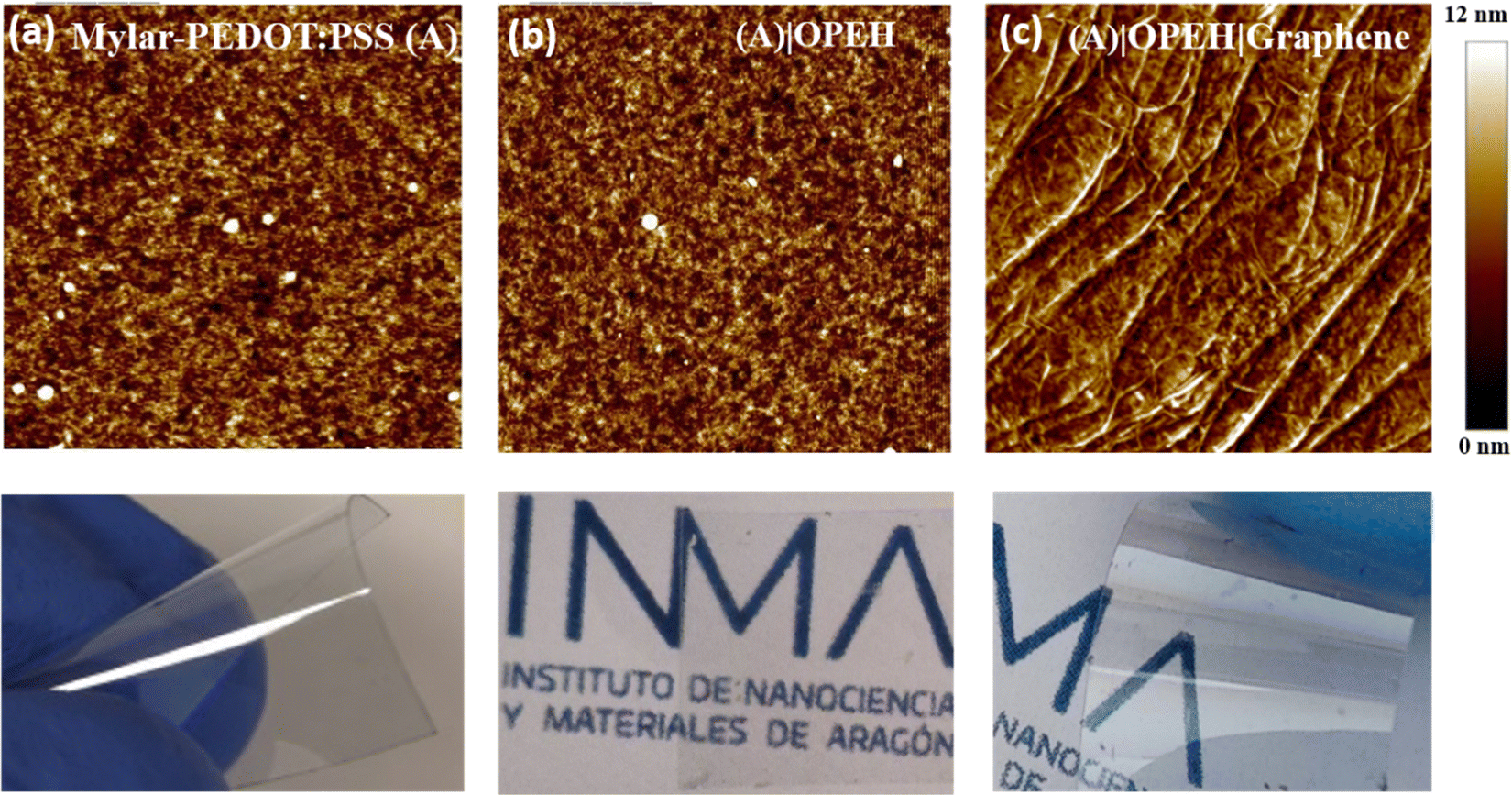 | ||
| Fig. 1 5 × 5 μm2 topography AFM images for (a) a Mylar–PEDOT:PSS, (b) Mylar–PEDOT:PSS|OPEH and (c) Mylar–PEDOT:PSS|OPEH|Graphene substrates. (bottom) Photographic images showing the high transparency and flexibility of the substrates along each of the steps of the fabrication. | ||
Electrografting process and characterization
A molecular monolayer was electrografted to the Mylar–PEDOT:PSS substrate by electroreduction of the in situ produced diazonium salt derived from 4-(4-(4-(trimethylsilylethynyl) phenylethynyl)phenylethynyl) aniline (1) following established methodologies.75–77 The substrate was incorporated into an electrochemical cell as the working electrode. The cell contained a solution whose concentration was 2.5 mM of 1, 7.5 mM in tert-butyl nitrite (tBuONO). I.e. the molecule:reducing agent ratio was 1:3, and 0.1 M in tetraethylammonium tetrafluoroborate (NEt4BF4,), with the potential repetitively cycling between +0.4 and −0.8 V (Fig. 2). The trimethylsilyl group sterically protects the growing monolayer from dendritic growth,62,78 and after each scan, the Mylar–PEDOT:PSS substrates modified by the growing monolayer were thoroughly rinsed in acetonitrile (ACN), and sonicated for 5 min in ACN, EtOH and acetone to remove the physisorbed material to improve the coverage of the surface in successive cycles. The decrease of the current associated with reduction of the diazonium salt formed from 1 (−0.35 V) in every cycle can be used to follow the deposition process. Three reduction and wash cycles were found optimum to deposit a film of 1 onto the Mylar–PEDOT:PSS substrate, with no further decrease in the diazonium reduction current observed in successive cycles (Fig. 2).
 | ||
| Fig. 2 Electrografting voltammograms for a 2.5 mM solution of 1 onto Mylar–PEDOT:PSS in ACN and 0.1 M NEt4BF4 as electrolyte at a scan rate of 50 mV s−1. | ||
After completion of the electrografting cycles, the trimethylsilyl (TMS) group was removed by immersing the grafted substrate in a methanolic solution of K2CO3 (50 mM) for 60 min, before being rinsed with ethanol and dried with a N2 flow to reveal the more chemically active terminal alkyne functionalised surface.79,80 The removal of the TMS group was demonstrated by absence of Si 2p peaks in the X-ray photoelectron spectrum (XPS) (Fig. S3, ESI†). The ethynyl-functionalised monolayer films offered a RMS surface roughness of (1.60 ± 0.04 nm), which is only slightly higher than the Mylar–PEDOT:PSS substrate (1.30 ± 0.06 nm) (Fig. 1a and b). Although the softness of the PEDOT:PSS film made it challenging to determine the thickness of the electrografted film by AFM tip pit etching, a 2.1 ± 0.2 nm thick film was deposited on a highly ordered pyrolytic graphite (HOPG) substrate from 1 by electrografting and elimination of the TMS group under the same conditions (Fig. S4, ESI†). This film thickness compares the length of the molecule (2.1 nm, calculated by Spartan 08 V1.0.0), and is consistent with the formation of an OPE-type monolayer under these experimental conditions. The resistivity of the modified bottom electrode was found to be of the same order of magnitude as that of the pristine PEDOT:PSS film, indicating little distortion of the electronic properties of the conducting polymer substrate as a result of the introduction of the electrografted monolayer. The similarity of Raman spectra recorded before and after the electrografting and deprotection processes, and particularly the PEDOT:PSS bands, indicate that the substrate is largely unaffected by the grafting of the monolayer (Fig. S5, ESI†).
Electrochemical electron transfer currents at electrodes under controlled potential provide an indirect measure of defect densities in thin films.81 Cyclic voltammograms (CVs) were obtained from aqueous solutions containing 1 mM K4[Fe(CN)6] and 0.1 M KCl using either a Mylar–PEDOT:PSS substrate or a Mylar–PEDOT:PSS substrate further modified by the ethynyl-terminated OPE monolayer derived from 1 (Mylar–PEDOT:PSS|OPEH) as the working electrode (Fig. S6, ESI†). The electrochemical response of a Mylar–PEDOT:PSS electrode exhibits a clear voltammetric wave for the ferrocyanide/ferricyanide couple. The electrografted electrode displays almost complete blocking behaviour, indicating a negligible distribution of holes or defects in the monolayer.
Graphene processing
The top-contact electrode was prepared from a graphene film grown by chemical vapour deposition (CVD) on Cu foils (Graphenea). A piece of the graphene-on-Cu-foil was cut to a size (ca. 0.7 × 0.6 cm) such as to only partially cover the Mylar–PEDOT:PSS|Monolayer stack (Fig. S7, ESI†). The graphene film was spin-coated with a PMMA thin film, before the underlying Cu support was removed by etching in a ferric chloride solution. The resulting PMMA|graphene film was thoroughly rinsed in deionized water before being placed onto the top surface of the assembling device stack. The assembly was annealed to improve adhesion of the graphene film and engineer good electrical contact. To prevent damage or deformation of the Mylar® substrate the annealing temperature was kept below 125 °C (the maximum service temperature recommended for Mylar® polyester film is 150 °C), instead of the more typically applied conditions (up to 180 °C).82 The PMMA transfer film was removed by immersing the large area device sequentially in acetone and isopropanol and allowed to dry on air. Fig. 1c shows an AFM image of the graphene layer deposited over Mylar–PEDOT:PSS|OPEH|Graphene substrate and a picture showing its transparency and flexibility.
For reference measurements, a simple, monolayer-free Mylar–PEDOT:PSS|Graphene stack was also constructed, using the same graphene transfer methods as described above and an unmodified Mylar–PEDOT:PSS substrate. The presence of small amounts of PMMA that were not removed during the processing of the graphene give rise to the bright spots in the AFM images of the surface (Fig. S8, ESI†). For both the Mylar–PEDOT:PSS|OPEH|Graphene (Fig. 1c) and Mylar–PEDOT:PSS| Graphene (Fig. S8, ESI†) device structures, the surface images also reveal shallow undulations or folds across the graphene sheet.
Electrical characterization
The electrical behaviour of the monolayer-free Mylar–PEDOT:PSS|Graphene device and large area Mylar–PEDOT:PSS|OPEH|Graphene molecular junction were determined from I–V curves recorded with a conductive atomic force microscope (c_AFM) in the Peak Force Tapping mode by positioning the PF-TUNA cantilever on top of the graphene layer. In the PF-TUNA mode, the tip makes intermittent contact with the surface at a frequency of 2 kHz and a low maximum force (peak-force). In this mode, both vertical and lateral forces on the sample surface are minimized, making PF-TUNA a valuable method for conductivity mapping of delicate samples.
The I–V characteristics of a monolayer-free Mylar–PEDOT:PSS|Graphene structure were determined by recording I–V plots at a set-point force of 10 nN. Most of the I–V plots exhibit linear behavior (ohmic response) over all range voltage ranges explored, eventually reaching saturation as the current exceeds the limits of the amplifier employed (Fig. S9, ESI†). Whilst these I–V plots show some variability in the slope of the ohmic response that could be due to non-uniform contact of the wrinkled graphene layer with the PEDOT:PSS layer, no traces of the sigmoidal shaped I–V curves that characterise through molecule conductance at high bias were observed.
Before recording the I–V curves of the Mylar–PEDOT:PSS|OPEH|Graphene structure, it was necessary to select a suitable set-point that achieves a compromise between a sufficiently large force to give a good electrical contact between the tip and the graphene top electrode, which is not preferred as it may result in deformation of the underlying monolayer (Fig. 3a). At set points below 7.5 nN, no significant current was detected above the background noise. For set-point forces higher than 7.5 nN (such as 11 and 15 nN), a more robust electrical contact is stablished between the tip and the graphene layer, leading to the sigmoidal-shaped I–V plots that characterize through molecule conductance (vide infra).
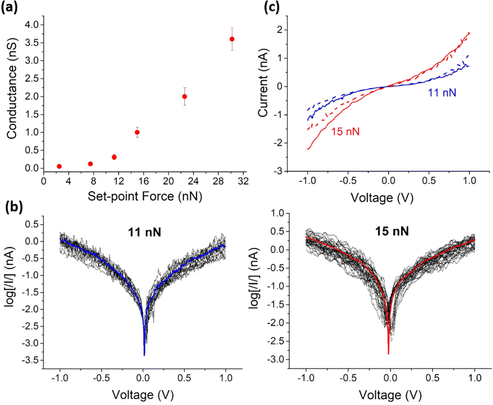 | ||
| Fig. 3 (a) Conductance values determined by locating the tip of the c-AFM onto the graphene layer versus the applied set point-force. (b) log[|I|] versus voltage for all I–V curves measured at a set point force of 11 (left) and 15 (right) nN. In blue and red line, the average curves. (c) Average I–V curves registered for a set-point force of 11 nN (blue line) and 15 nN (red line) and after folding the Mylar–PEDOT:PSS|OPEH|Graphene system (dashed lines). | ||
In contrast to the sigmoidal I–V response collected from the monolayer device by PF-TUNA at low set-point forces, as the set-point force increases (22 or 30 nN), high conductance values with linear (ohmic) response to increases in voltage are obtained. This change in the I–V characteristics is probably due to the tip pressing the graphene top-contact into the soft, supporting monolayer, resulting in considerable deformation of the structure or even direct contact between the graphene and substrate PEDOT:PSS layer.
Set points between 11 and 15 nN were therefore selected as points of the minimum force require to achieve electrical contact, and 150 I–V curves recorded at each set point (with each set of curves containing data recorded from multiple areas from each of several different devices (Fig. 3b)). Importantly, these curves show a linear response at relatively low bias voltages with the characteristic molecular sigmoidal shape emerging at higher bias (Fig. 3c); none of the data collected gave any indication of short circuits through the electrografted mono-layer large-area devices. Importantly, the observed variation of less than half an order of magnitude in the currents obtained from all the recorded I–V curves (Fig. 3b) demonstrate the reproducibility of the monolayer device structure. These differences in the I–V response of the monolayer-free Mylar–PEDOT:PSS|Graphene device and large area Mylar–PEDOT:PSS|OPEH|Graphene molecular junction collected at these moderate set-point forces are attributed to the through-molecule conductance characteristics of the monolayer versus the PEDOT:PSS|Graphene interface.
The c-AFM study reveals a strong dependence of the molecular conductance of the large area devices reported here with set-point force, before the device breaks down into an ohmic regime. This observation contributes to the inherent difficulties associated with comparisons of the conductance values of large-areas devices with the single molecule conductance of similar materials with the estimated conductance per molecule in large area junctions often found to be 8–9 orders of magnitude smaller than the measurements obtained from single- and few-molecule-junctions.83–85 These differences can be attributed to any one or a combination of factors that pertain to the subtle physical and electrical differences associated with single-molecule and large-area junctions, and the challenges in distinguishing the effective electrical contact area from the geometrical contact area of a large probe tip.85–87 Akkerman and colleagues have also noted that the estimated conductance per molecule progressively decreases with increasing junction area,83 which likely reflects these variations in molecule–electrode contact phenomena.
For a molecular junction, the effective tunnel barrier height and molecule–electrode electronic coupling (and hence junction conductance) are both strongly influenced by the work function of the electrodes, and even in a single-molecule junction, molecular conductance can vary by several orders of magnitude depending on the electrode material. The different electrodes commonly used in single-molecule and large-area junction measurements should therefore also be considered when attempting to draw direct comparisons of per-molecule conductance values.88–90 Of course, changes in electrode material can be further accompanied by changes in the nature of the molecule–electrode contact (chemisorbed vs. physisorbed) that substantively modulate molecule–electrode coupling. The top-contact electrode used here (graphene) is deposited by physical contact on top of the monolayer and physisorbs to the molecular monolayer through the terminal alkyne terminal group. When the AFM tip makes contact with the graphene, the pressure is distributed across the graphene and the PEDOT:PSS|OPEH substrate in a radically different manner than would be the case for a chemisorbed layer. It influences the electron transfer through the graphene and also the effective contact area. The dependence of conductance as a function of set-point force indicates the interplay between tip pressure and electron transfer. In the particular case of monolayer graphene electrodes, the non-uniform contact of the graphene to the underlying substrate, as illustrated by the surface images presented here (Fig. 1c), further complicates the data extracted from average measurements from sampling across large area junctions. The challenges to engineering good electrical contact to graphene surfaces in molecular electronics are recognised, and future generations of this design strategy which enhance molecule–graphene coupling at the top electrode interface are being explored.91–93
Since the Mylar–PEDOT:PSS|OPEH|Graphene substrate is transparent and flexible (Fig. 1c), one important question to be addressed is whether the electrical properties are preserved after folding the device. The electrical properties of a Mylar–PEDOT:PSS|OPEH|Graphene substrate were determined after folding it manually (ca. 180°, Fig. 1a) and allowing it to recover its initial state. This procedure was repeated three times before recording the I–V curves. These curves show again a linear section at relatively low bias voltages with the characteristic molecular sigmoidal shape at higher bias (Fig. 3c, Fig. S10, ESI†). It is also important to note that the average curves at each set point are practically the same to the ones obtained for the same substrate before folding. These preliminary results demonstrate the reliability of the electrical properties of this device, albeit with acknowledgement that further studies are required to establish tolerance limits and point of device failure.
Conclusions
A transparent, flexible and conductive electrode based on a Mylar®-supported PEDOT:PSS film has been fabricated and used as a substrate–bottom electrode upon which an homogenous monolayer of a OPE derivative was electrografted. Graphene was deposited by wet transfer on top of the Mylar–PEDOT:PSS|OPEH structure, with I–V curves recorded by positioning the tip of a conductive AFM on top of the graphene layer showing electrical behavior characteristic of electrode|molecule|electrode junctions (linear section at relatively low bias voltages and an increase of the curvature at higher bias) ruling out the presence of short circuits. Therefore, the use of Mylar®, as a flexible and transparent support, to deposit PEDOT:PSS (bottom contact electrode) over which to electrografting an organic monolayer in combination with a wet transfer of graphene onto this layer (top contact electrode), open new possibilities for the development of a future optoelectronics technology.
Conflicts of interest
There are no conflicts to declare.Acknowledgements
P. C. and S. M. acknowledge PID2019-105881RB-I00 (MCIN/AEI/10.13039/501100011033), PID2022-14143300B-I00 and TED2021-131318B-I00 grant funded by the MCIN/AEI/10.13039/501100011033 and “European Union NextGenerationEU/PRTR”. These authors also acknowledge DGA/Fondos FEDER (Construyendo Europa desde Aragón) for funding the research group Platón (E31-23R). H. M. O. is grateful for financial assistance from Escuela Politécnica Nacional in the framework of project PIGR-19-04. G. R. acknowledges her contract under the programme Ayudas Ramon y Cajal, Reference RYC-2016-21412. P. J. L. gratefully acknowledges support from the Australian Research Council (DP220100790).References
- B. F. Zeng, Y. L. Zou, G. Wang, W. J. Hong, Z. Q. Tian and Y. Yang, Nano Today, 2022, 47, 101660 CrossRef CAS.
- X. M. Xie, P. H. Li, Y. X. Xu, L. Zhou, Y. H. Yan, L. H. Xie, C. C. Jia and X. F. Guo, ACS Nano, 2022, 16, 3476–3505 CrossRef CAS PubMed.
- H. L. Chen, C. C. Jia, X. Zhu, C. Yang, X. F. Guo and J. F. Stoddart, Nat. Rev. Mater., 2023, 8, 165–185 CrossRef.
- R. Gupta, J. A. Fereiro, A. Bayat, A. Pritam, M. Zharnikov and P. C. Mondal, Nat. Rev. Chem., 2023, 7, 106–122 CrossRef CAS PubMed.
- N. Xin, J. X. Guan, C. G. Zhou, X. J. N. Chen, C. H. Gu, Y. Li, M. A. Ratner, A. Nitzan, J. F. Stoddart and X. F. Guo, Nat. Rev. Phys., 2019, 1, 211–230 CrossRef.
- V. Dubois, S. N. Raja, P. Gehring, S. Caneva, H. S. J. van der Zant, F. Niklaus and G. Stemme, Nat. Commun., 2018, 9, 3433 CrossRef PubMed.
- J. He, O. Sankey, M. Lee, N. J. Tao, X. L. Li and S. Lindsay, Faraday Discuss., 2006, 131, 145–154 RSC.
- M. A. Reed, C. Zhou, C. J. Muller, T. P. Burgin and J. M. Tour, Science, 1997, 278, 252–254 CrossRef CAS.
- B. Q. Xu and N. J. J. Tao, Science, 2003, 301, 1221–1223 CrossRef CAS PubMed.
- E. M. Dief, P. J. Low, I. Diez-Perez and N. Darwish, Nat. Chem., 2023, 15, 600–614 CrossRef CAS PubMed.
- E. Gorenskaia, K. L. Turner, S. Martin, P. Cea and P. J. Low, Nanoscale, 2021, 13, 9055–9074 RSC.
- L. Herrer, S. Martin and P. Cea, Appl. Sci., 2020, 10, 6064 CrossRef CAS.
- J. Shin, J. S. Eo, T. Jeon, T. Lee and G. Wang, Adv. Sci., 2022, 9, 2202399 CrossRef PubMed.
- A. Vilan, D. Aswal and D. Cahen, Chem. Rev., 2017, 117, 4248–4286 CrossRef CAS PubMed.
- D. Xiang, X. L. Wang, C. C. Jia, T. Lee and X. F. Guo, Chem. Rev., 2016, 116, 4318–4440 CrossRef CAS PubMed.
- H. B. Akkerman, P. W. M. Blom, D. M. de Leeuw and B. de Boer, Nature, 2006, 441, 69–72 CrossRef CAS PubMed.
- J. M. Beebe, V. B. Engelkes, L. L. Miller and C. D. Frisbie, J. Am. Chem. Soc., 2002, 124, 11268–11269 CrossRef CAS PubMed.
- G. K. Ramachandran, T. J. Hopson, A. M. Rawlett, L. A. Nagahara, A. Primak and S. M. Lindsay, Science, 2003, 300, 1413–1416 CrossRef CAS PubMed.
- Q. Lu, K. Liu, H. M. Zhang, Z. B. Du, X. H. Wang and F. S. Wang, ACS Nano, 2009, 3, 3861–3868 CrossRef CAS PubMed.
- A. C. Aragones, N. Darwish, S. Ciampi, F. Sanz, J. J. Gooding and I. Diez-Perez, Nat. Commun., 2017, 8, 15056 CrossRef CAS PubMed.
- X. T. Wang, S. Sangtarash, A. Lamantia, H. Dekkiche, L. Forcieri, O. V. Kolosov, S. P. Jarvis, M. R. Bryce, C. J. Lambert, H. Sadeghi and B. J. Robinson, J. Phys. Energy, 2022, 4, 024002 CrossRef.
- O. N. Oliveira, L. Caseli and K. Ariga, Chem. Rev., 2022, 122, 6459–6513 CrossRef PubMed.
- L. Herrer, S. Martin, A. Gonzalez-Orive, D. C. Milan, A. Vezzoli, R. J. Nichols, J. L. Serrano and P. Cea, J. Mater. Chem. C, 2021, 9, 2882–2889 RSC.
- E. Escorihuela, P. Cea, S. Bock, D. C. Milan, S. Naghibi, H. M. Osorio, R. J. Nichols, P. J. Low and S. Martin, J. Mater. Chem. C, 2020, 8, 672–682 RSC.
- E. Escorihuela, A. Concellon, I. Marin, V. J. Kumar, L. Herrer, S. A. Moggach, A. Vezzoli, R. J. Nichols, P. J. Low, P. Cea, J. L. Serrano and S. Martin, Mater. Today Chem., 2022, 26, 101067 CrossRef CAS.
- A. J. Bergren, K. D. Harris, F. J. Deng and R. L. McCreery, J. Phys.: Condens. Matter., 2008, 20, 374117 CrossRef PubMed.
- J. C. Lacroix, Curr. Opin. Electrochem., 2018, 7, 153–160 CrossRef CAS.
- A. P. Bonifas and R. L. McCreery, Nat. Nanotechnol., 2010, 5, 612–617 CrossRef CAS PubMed.
- P. Hapiot, C. Lagrost and Y. R. Leroux, Curr. Opin. Electrochem., 2018, 7, 103–108 CrossRef CAS.
- M. V. Sulleiro, A. Develioglu, R. Quiros-Ovies, L. Martin-Perez, N. M. Sabanes, M. L. Gonzalez-Juarez, I. J. Gomez, M. Vera-Hidalgo, V. Sebastian, J. Santamaria, E. Burzuri and E. M. Perez, Nat. Chem., 2022, 14, 695–700 CrossRef PubMed.
- A. Martin-Barreiro, R. Soto, S. Chiodini, A. Garcia-Serrano, S. Martin, L. Herrer, F. Perez-Murano, P. J. Low, J. L. Serrano, S. Marcos, J. Galban and P. Cea, Adv. Mater. Interfaces, 2021, 8, 2100876 CrossRef CAS.
- H. Haick and D. Cahen, Prog. Surf. Sci., 2008, 83, 217–261 CrossRef CAS.
- L. M. Ballesteros, S. Martin, J. Cortes, S. Marques-Gonzalez, F. Perez-Murano, R. J. Nichols, P. J. Low and P. Cea, Adv. Mater. Interfaces, 2014, 1, 1400128 CrossRef.
- L. Herrer, V. Sebastian, S. Martin, A. Gonzalez-Orive, F. Perez-Murano, P. J. Low, J. L. Serrano, J. Santamaria and P. Cea, Nanoscale, 2017, 9, 13281–13290 RSC.
- H. M. Osorio, P. Cea, L. M. Ballesteros, I. Gascon, S. Marques-Gonzalez, R. J. Nichols, F. Perez-Murano, P. J. Low and S. Martin, J. Mater. Chem. C, 2014, 2, 7348–7355 RSC.
- T. Li, J. R. Hauptmann, Z. M. Wei, S. Petersen, N. Bovet, T. Vosch, J. Nygard, W. P. Hu, Y. Q. Liu, T. Bjornholm, K. Norgaard and B. W. Laursen, Adv. Mater., 2012, 24, 1333–1339 CrossRef CAS PubMed.
- J. Koo, Y. Jang, L. Martin, D. Kim, H. Jeong, K. Kang, W. Lee, J. Kim, W. T. Hwang, D. Xiang, E. Scheer, M. Kabdulov, T. Huhn, F. Pauly and T. Lee, ACS Appl. Mater. Interfaces, 2019, 11, 11645–11653 CrossRef CAS PubMed.
- D. Kim, H. Jeong, W. T. Hwang, Y. Jang, D. Sysoiev, E. Scheer, T. Huhn, M. Min, H. Lee and T. Lee, Adv. Funct. Mater., 2015, 25, 5918–5923 CrossRef CAS.
- R. Kumar, H. J. Yan, R. L. McCreery and A. J. Bergren, Phys. Chem. Chem. Phys., 2011, 13, 14318–14324 RSC.
- S. Sangiao, S. Martin, A. Gonzalez-Orive, C. Magen, P. J. Low, J. M. de Teresa and P. Cea, Small, 2017, 13, 1603207 CrossRef PubMed.
- K. S. Wimbush, R. M. Fratila, D. D. Wang, D. C. Qi, C. Liang, L. Yuan, N. Yakovlev, K. P. Loh, D. N. Reinhoudt, A. H. Velders and C. A. Nijhuis, Nanoscale, 2014, 6, 11246–11258 RSC.
- A. Wan, L. Jiang, C. S. S. Sangeeth and C. A. Nijhuis, Adv. Funct. Mater., 2014, 24, 4442–4456 CrossRef CAS.
- D. Gutierrez, J. A. de Sousa, M. Mas-Torrent and N. Crivillers, ACS Appl. Electron. Mater., 2020, 2, 3093–3099 CrossRef CAS.
- R. M. Metzger, T. Xu and I. R. Peterson, J. Phys. Chem. B, 2001, 105, 7280–7290 CrossRef CAS.
- Y. N. Xia and G. M. Whitesides, Angew. Chem., Int. Ed., 1998, 37, 550–575 CrossRef CAS PubMed.
- D. Guerin, C. Merckling, S. Lenfant, X. Wallart, S. Pleutin and D. Vuillaume, J. Phys. Chem. C, 2007, 111, 7947–7956 CrossRef CAS.
- T. Baunach, V. Ivanova, D. M. Kolb, H. G. Boyen, P. Ziemann, M. Buttner and P. Oelhafen, Adv. Mater., 2004, 16, 2024 CrossRef CAS.
- G. L. Fisher, A. E. Hooper, R. L. Opila, D. L. Allara and N. Winograd, J. Phys. Chem. B, 2000, 104, 3267–3273 CrossRef CAS.
- G. Nagy and A. V. Walker, J. Phys. Chem. C, 2007, 111, 8543–8556 CrossRef CAS.
- G. Puebla-Hellmann, K. Venkatesan, M. Mayor and E. Lortscher, Nature, 2018, 559, 232–235 CrossRef CAS PubMed.
- A. M. Najarian, B. Szeto, U. M. Tefashe and R. L. McCreery, ACS Nano, 2016, 10, 8918–8928 CrossRef PubMed.
- U. M. Tefashe, Q. Van Nguyen, F. Lafolet, J. C. Lacroix and R. L. McCreery, J. Am. Chem. Soc., 2017, 139, 7436–7439 CrossRef CAS PubMed.
- S. Seo, M. Min, S. M. Lee and H. Lee, Nat. Commun., 2013, 4, 1920 CrossRef PubMed.
- B. W. Yao, L. S. de Vasconcelos, Q. Y. Cui, A. Cardenas, Y. C. Yan, Y. J. Du, D. Wu, S. W. Wu, T. K. Hsiai, N. S. Lu, X. Y. Zhu and X. M. He, Mater. Today, 2022, 53, 84–97 CrossRef CAS.
- G. J. Adekoya, R. E. Sadiku and S. S. Ray, Macromol. Mater. Eng., 2021, 306, 2000716 CrossRef CAS.
- S. D. Xu, M. Hong, X. L. Shi, Y. Wang, L. Ge, Y. Bai, L. Z. Wang, M. Dargusch, J. Zou and Z. G. Chen, Chem. Mater., 2019, 31, 5238–5244 CrossRef CAS.
- L. V. Kayser and D. J. Lipomi, Adv. Mater., 2019, 31, 1806133 CrossRef PubMed.
- Y. Zheng, H. N. Zeng, Q. Zhu and J. W. Xu, J. Mater. Chem. C, 2018, 6, 8858–8873 RSC.
- Z. M. Yu, Y. J. Xia, D. H. Du and J. Y. Ouyang, ACS Appl. Mater. Interfaces, 2016, 8, 11629–11638 CrossRef CAS PubMed.
- A. J. Bergren, R. L. McCreery, S. R. Stoyanov, S. Gusarov and A. Kovalenko, J. Phys. Chem. C, 2010, 114, 15806–15815 CrossRef CAS.
- H. J. Yan, A. J. Bergren and R. L. McCreery, J. Am. Chem. Soc., 2011, 133, 19168–19177 CrossRef CAS PubMed.
- S. Y. Sayed, A. Bayat, M. Kondratenko, Y. Leroux, P. Hapiot and R. L. McCreery, J. Am. Chem. Soc., 2013, 135, 12972–12975 CrossRef CAS PubMed.
- H. Song, X. Y. Zhang, Y. F. Liu and Z. Q. Su, Chem. Rec., 2019, 19, 534–549 CrossRef CAS PubMed.
- D. G. Papageorgiou, I. A. Kinloch and R. J. Young, Prog. Mater. Sci., 2017, 90, 75–127 CrossRef CAS.
- C. C. Jia, B. J. Ma, N. Xin and X. F. Guo, Acc. Chem. Res., 2015, 48, 2565–2575 CrossRef CAS PubMed.
- Q. Zhang, L. L. Liu, S. H. Tao, C. Y. Wang, C. Z. Zhao, C. Gonzalez, Y. J. Dappe, R. J. Nichols and L. Yang, Nano Lett., 2016, 16, 6534–6540 CrossRef CAS PubMed.
- G. Pera, S. Martín, L. M. Ballesteros, A. J. Hope, P. J. Low, R. J. Nichols and P. Cea, Chem. – Eur. J., 2010, 16, 13398–13405 CrossRef CAS PubMed.
- M. Mozetic, Polymers, 2020, 12, 2498 CrossRef CAS PubMed.
- I. Junkar, M. Modic and M. Mozeti, Open Chem., 2015, 13, 490–496 Search PubMed.
- A. E. Abusrafa, S. Habib, I. Krupa, M. Ouederni and A. Popelka, Coatings, 2019, 9, 145 CrossRef.
- A. Håkansson, S. Han, S. Wang, J. Lu, S. Braun, M. Fahlman, M. Berggren, X. Crispin and S. Fabiano, J. Polym. Sci., Part B: Polym. Phys., 2017, 55, 814–820 CrossRef.
- S. Zhang, P. Kumar, A. S. Nouas, L. Fontaine, H. Tang and F. Cicoira, APL Mater., 2015, 3, 014911 CrossRef.
- N. A. Shahrim, Z. Ahmad, A. W. Azman, Y. F. Buys and N. Sarifuddin, Mater. Adv., 2021, 2, 7118–7138 RSC.
- J. Huang, P. F. Miller, J. C. de Mello, A. J. de Mello and D. D. C. Bradley, Synth. Met., 2003, 139, 569–572 CrossRef CAS.
- M. Delamar, R. Hitmi, J. Pinson and J. M. Saveant, J. Am. Chem. Soc., 1992, 114, 5883–5884 CrossRef CAS.
- V. Stockhausen, G. Trippe-Allard, N. V. Quynh, J. Ghilane and J. C. Lacroix, J. Phys. Chem. C, 2015, 119, 19218–19227 CrossRef CAS.
- M. Supur, C. Van Dyck, A. J. Bergren and R. L. McCreery, ACS Appl. Mater. Interfaces, 2018, 10, 6090–6095 CrossRef CAS PubMed.
- Y. R. Leroux, H. Fei, J. M. Noel, C. Roux and P. Hapiot, J. Am. Chem. Soc., 2010, 132, 14039–14041 CrossRef CAS PubMed.
- A. Moneo, A. Gonzalez-Orive, S. Bock, M. Fenero, I. L. Herrer, D. C. Milan, M. Lorenzoni, R. J. Nichols, P. Cea, F. Perez-Murano, P. J. Low and S. Martin, Nanoscale, 2018, 10, 14128–14138 RSC.
- Y. C. Fu, S. J. Chen, A. Kuzume, A. Rudnev, C. C. Huang, V. Kaliginedi, M. Baghernejad, W. J. Hong, T. Wandlowski, S. Decurtins and S. X. Liu, Nat. Commun., 2015, 6, 6403 CrossRef CAS PubMed.
- M. D. Porter, T. B. Bright, D. L. Allara and C. E. D. Chidsey, J. Am. Chem. Soc., 1987, 109, 3559–3568 CrossRef CAS.
- F. Zummo, P. Esposito, H. L. Hou, C. Wetzl, G. Rius, R. Tkatchenko, A. Guimera, P. Godignon, M. Prato, E. Prats-Alfonso, A. Criado and D. Scaini, Front. Neurosci., 2022, 15, 811348 CrossRef PubMed.
- H. B. Akkerman and B. de Boer, J. Phys.: Condens. Matter, 2008, 20, 013001 CrossRef.
- F. Milani, C. Grave, V. Ferri, P. Samori and M. A. Rampi, Chem. Phys. Chem., 2007, 8, 515–518 CrossRef CAS PubMed.
- B. Li, M. Famili, E. Pensa, I. Grace, N. J. Long, C. Lambert, T. Albrecht and L. F. Cohen, Nanoscale, 2018, 10, 19791–19798 RSC.
- C. S. S. Sangeeth, A. T. Demissie, L. Yuan, T. Wang, C. D. Frisbie and C. A. Nijhuis, J. Am. Chem. Soc., 2016, 138, 7305–7314 CrossRef CAS PubMed.
- F. C. Simeone, H. J. Yoon, M. M. Thuo, J. R. Barber, B. Smith and G. M. Whitesides, J. Am. Chem. Soc., 2013, 135, 18131–18144 CrossRef CAS PubMed.
- B. Kim, S. H. Choi, X. Y. Zhu and C. D. Frisbie, J. Am. Chem. Soc., 2011, 133, 19864–19877 CrossRef CAS PubMed.
- M. J. Huang, L. Y. Hsu, M. D. Fu, S. T. Chuang, F. W. Tien and C. H. Chen, J. Am. Chem. Soc., 2014, 136, 1832–1841 CrossRef CAS PubMed.
- T. Kim, Z. F. Liu, C. Lee, J. B. Neaton and L. Venkataraman, Proc. Natl. Acad. Sci. U. S. A., 2014, 111, 10928–10932 CrossRef CAS PubMed.
- C. Yang, C. Y. Yang, Y. L. Guo, J. F. Feng and X. F. Guo, Nat. Protoc., 2023, 18, 1958–1978 CrossRef CAS PubMed.
- J. Trasobares, J. C. Martín-Romano, M. W. Khaliq, S. Ruiz-Gómez, M. Foerster, M. A. Niño, P. Pedraz, Y. J. Dappe, M. C. de Ory, J. García-Pérez, M. Acebrón, M. R. Osorio, M. T. Magaz, A. Gomez, R. Miranda and D. Granados, Nat. Commun., 2023, 14, 1381 CrossRef CAS PubMed.
- S. H. Hong, D. H. Seo and H. Song, Crystals, 2022, 12, 787 CrossRef CAS.
Footnote |
| † Electronic supplementary information (ESI) available. See DOI: https://doi.org/10.1039/d3tc02237d |
| This journal is © The Royal Society of Chemistry 2024 |