DOI:
10.1039/D4MH00322E
(Communication)
Mater. Horiz., 2024,
11, 3330-3344
A polarization double-enhancement strategy to achieve super low energy consumption with ultra-high energy storage capacity in BCZT-based relaxor ferroelectrics†
Received
21st March 2024
, Accepted 11th April 2024
First published on 12th April 2024
Abstract
Due to dielectric capacitors’ already-obtained fast charge–discharge speed, research has been focused on improving their Wrec. Increasing the polarization and enhancing the voltage endurance are efficient ways to reach higher Wrec, however simultaneous modification still seems a paradox. For example, in the ferroelectric-to-relaxor ferroelectric (FE-to-RFE) phase transition strategy, which has been widely used in the latest decade, electric breakdown strength (Eb) and energy storage efficiency (η) always increase, while at the same time, the maximum polarization (Pmax) inevitably decreases. The solution to this problem can be obtained from another degree of freedom, like defect engineering. By incorporating Bi(Zn2/3Ta1/3)O3 (BZT) into the Ba0.15Ca0.85Zr0.1Ti0.9O3 (BCZT) lattice to form (1 − x)Ba0.15Ca0.85Zr0.1Ti0.9O3–xBi(Zn2/3Ta1/3)O3 (BCZT–xBZT) solid-solution ceramics, in this work, ultrahigh ferroelectric polarization was achieved in BCZT–0.15BZT, which is caused by the polarization double-enhancement, comprising the contribution of interfacial and dipole polarization. In addition, due to the electron compensation, a Schottky contact formed at the interface between the electrode and the ceramic, which in the meantime, enhanced its Eb. A Wrec of 8.03 J cm−3, which is the highest among the BCZT-based ceramics reported so far, with an extremely low energy consumption, was finally achieved. BCZT–0.15BZT also has relatively good polarization fatigue after long-term use, good energy storage frequency stability and thermal stability, as well as excellent discharge properties.
New concepts
Rather than simply increasing the energy storage density/efficiency of dielectric capacitors, as reported in most studies, in this work, a fancy strategy of polarization double-enhancement has been demonstrated for a BCZT-based energy storage ferroelectric with super low consumption. By finely regulating the components, both dipole polarization and interfacial polarization were confirmed in BCZT–xBZT with x = 0.15, combined with the Schottky emission mode between the ceramic and the electrode, which helped to increase the voltage endurance, thus an ultrahigh energy storage density of 8.03 J cm−3 with an extremely low energy-consumption was achieved. This is the highest energy storage performance in a BCZT-based ferroelectric, as far as the authors know. Such a good result was also revealed by employing the finite element simulation. In this work, we solve the paradox of increasing the difference between Pmax and Pr and enhancing the Eb in dielectric capacitors simultaneously via adding defect engineering to the domain engineering during the FE-to-RFE phase transition. It will inspire researchers to modify the properties of functional materials by combining the parameters from different degrees of freedom.
|
1. Introduction
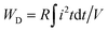
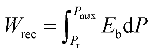
Dielectric energy storage capacitors, which are considered the most promising candidates for next-generation high-power systems, have attracted considerable research attention in recent decades due to their superfast charge–discharge speed and good reliability after long-term use.1–12 According to the Ragone plots displayed in Fig. S1 (ESI†), however, no single energy storage device can simultaneously possess high energy storage density (Wrec) and power density (Pd), commonly regarded as two key figures-of-merit of power systems. Obviously, increasing Wrec is becoming increasingly urgent for dielectric capacitors. Wrec can be calculated using:| |  | (1) |
in which Pmax, Pr, and Eb are the maximum polarization, remnant polarization, and electric breakdown strength, respectively. More details on calculating the energy storage parameters can be found in the ESI.† To increase Wrec, it is easy to understand that improving the difference between Pmax and Pr and enhancing Eb should be the two most conventional routes; however, simultaneously modifying them still seems to be a paradox.13–15
Utilizing domain engineering to achieve relaxor ferroelectrics (RFEs) is a popular strategy to achieve high Wrec, and recently, many researchers have benefited from this. Chu et al. doped La ions into BNT–BT ceramics to break the long-range order in ferroelectric domains to promote the formation of polar nano regions (PNRs) and a good Wrec of ∼5.93 J cm−3 with an energy storage efficiency (η) of ∼77.6% was thus achieved.16 Using the phase field method, in Li et al.'s work, a specific temperature region between the temperature of the maximum dielectric constant (ε) and the Burns temperature was moved to room temperature to induce the PNRs, together with repeating the rolling process for enhancing Eb, and a high Wrec of 6.7 J cm−3 with an η of 92% was achieved.17 For antiferroelectric (AFE) systems, such a strategy is also applicable. Wang et al. introduced a BiFeO3–SrTiO3 binary solid solution into pure NN ceramics, the tolerance factor (t) was reduced, and the AFE phase was stabilized simultaneously, increasing the Wrec value to 5.29 J cm−3 with an η of 82.1%,18 whereas during the phase transition from the typical ferroelectric (FE) or AFE to RFE, as in the abovementioned research, the polarization inevitably decreases, and thus, the energy storage capacity improvement is more or less limited. Regrettably, such a paradox has not been solved until now, and the solution seems to be obtained from another degree of freedom. Defect engineering is an effective way of obtaining high polarization in either ferroelectrics or linear dielectrics.19 For example, by co-doping Nb and Zn into SrTiO3 ceramics, defect complexes were induced with the localization of electrons, and giant ε and relatively low dielectric loss (tan![[thin space (1/6-em)]](https://www.rsc.org/images/entities/char_2009.gif) δ) were both achieved.20 Through rare-earth doping, colossal-permittivity (CP) BaTiO3 with ε as high as 105 and excellent temperature stability was obtained due to electron-pinned defect-dipole formation and strong hopping polarization.21 As for improving the energy storage properties, Lin et al. utilized A-site non-stoichiometric defect engineering to boost the energy storage performance of KNN-based ceramics successfully, and the existence of vacancy-related defects was revealed to be the main reason for the improvement.22 Therefore, such a paradox can be theoretically solved if these two strategies can be appropriately combined.
δ) were both achieved.20 Through rare-earth doping, colossal-permittivity (CP) BaTiO3 with ε as high as 105 and excellent temperature stability was obtained due to electron-pinned defect-dipole formation and strong hopping polarization.21 As for improving the energy storage properties, Lin et al. utilized A-site non-stoichiometric defect engineering to boost the energy storage performance of KNN-based ceramics successfully, and the existence of vacancy-related defects was revealed to be the main reason for the improvement.22 Therefore, such a paradox can be theoretically solved if these two strategies can be appropriately combined.
According to most of the recent studies on energy storage capacitors, which mainly focus on improving the absolute Wrec value by improving the Pmax and Eb values, achieving higher Wrec under relatively low electric fields is sometimes more important. Because high storage energy density are not always necessarily be achieved in practical energy-storing devices, reducing energy consumption becomes very important.23,24 In this work, dipole polarization, which is caused by the newly formed dipoles TaTi–Ti3+, was subtly induced during the FE-to-RFE phase transition of (1 − x)Ba0.15Ca0.85Zr0.1Ti0.9O3–xBi(Zn2/3Ta1/3)O3(BCZT–xBZT) ceramics with increasing x. In addition to the intrinsic interfacial polarization from the T-phase and C-phase coexistence, very high polarization was triggered in the BCZT–0.15BZT ceramic with x = 0.15. By employing the defect equation, an electron compensation mechanism was found to overcome such a charge imbalance, resulting in a Schottky emission mode in the interface between the electrode and the ceramic in BCZT–0.15BZT in a higher electric field range. With the assistance of the polynomial fit function in the Origin software and the finite element simulation in the COMSOL Multiphysics 6.0 linking with Matlab 5.2, such a Schottky emission mode was revealed to show a blocking behavior to the current spread, which is considered to be the origin of its optimistic Eb. Due to these, the highest Wrec value among BCZT-based ceramics so far, with extremely low energy consumption and high energy storage reliability, was obtained in our work.
2. Experimental section
Details of this part are provided in the ESI.†
3. Results and discussion
3.1 Phase and structure characterization
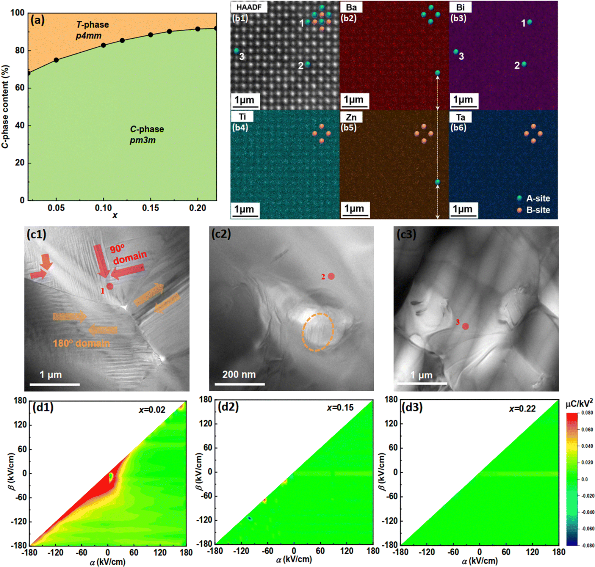
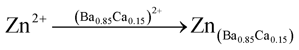
The BCZT–xBZT ceramics with x from 0.02 to 0.22 show a single-perovskite structure without any detectable impurities, as seen in their X-ray diffraction (XRD) patterns shown in Fig. S1(b1) (ESI†), in which every diffraction peak is indexed. A little difference can be distinguished in the enlarged view around the (200)/(002) plane in Fig. S1(b2) (ESI†). With the increasing BZT dopant, the peak shifts to a lower angle, and a similar phenomenon is then observed in all the peaks, demonstrating a lattice expansion. In addition, the (200)/(002) signal exhibits a shape transformation from an asymmetrical peak to a symmetrical one, which reflects a phase, or at least a structure transition in such a process. For a deeper analysis of such a transition, the Rietveld XRD refinement was carried out from the diffraction angle of 10° to 120°, and the result is displayed in Fig. S2(a1)–(a8) (ESI†). Details of the refinement parameters are listed in Table S1 (ESI†), and according to the Rwp, Rp, and χ2 values, which represent the weighted profile parameter, unweighted profile parameter, and the goodness of fit of each sample, respectively, such a refinement is highly credible. Based on the results, all these BCZT–xBZT ceramics show the coexistence of two phases with the space groups of the P4mm (T-phase) and the Pm3m (C-phase), and a ball-stick model of each one is illustrated in Fig. S2(b1) and (b2) (ESI†). As marked, the red spheres on each apex of the oxygen octahedron represent oxygen atoms, and the green and blue atoms outside of and in the octahedron represent the A-site and B-site atoms, respectively. The atom substitution is described by the spherical sectors. For the ball-stick model of P4mm, more space along the c-axis in the oxygen octahedron for the B-side atoms can be observed, indicating a higher polarization, while that for Pm3m is relatively small. Table S1 (ESI†) also lists the phase content ratio, and a phase diagram can be thus drawn, as illustrated in Fig. 1(a). As seen, though the content of the T-phase in the BCZT–xBZT ceramics decreases monotonously with increasing x from 0.02 to 0.22, it is worth noting that the structure of pristine BCZT and BZT is still unclear. The phase characterization results demonstrate that BZT was successfully incorporated into the BCZT lattice. For further exploring the atom substitution, the high-angle annular dark field scanning transmission electron microscopy (HAADF-STEM) image of BCZT–0.15BZT was obtained, as shown in Fig. 1(b1), and the corresponding energy dispersive spectroscopy (EDS) maps for the elements of Ba, Bi, Ti, Zn, and Ta are displayed in Fig. 1(b2)–(b6), respectively. By comparing the atom positions, Zn and Ta atoms mainly occupy the B-site to replace the Ti and Zr atoms. In contrast, the Bi atoms are more likely to take the A-site positions to substitute the Ba and Ca atoms, which agrees well with the previous study. (Due to our sample's poor conductivity, the slice's ion-milled area kept jiggling under the hit of the electron beam without staying stable during the measurement; thus not enough signals could be observed in the EDS maps obtained. Despite this, a signal for atoms 1–3 in Fig. 1(a1) and (a3) could still confirm the A-site substitution of the Bi atom.) Interestingly, in the mapping for Zn, a small number of A-sites also seem to be occupied by aligning with the position of Ba. More information on this will be discussed in the following part.25 The valence, coordination, and ionic radii of Ba, Ca, Bi, Zr, Ti, Zn, and Ta are summarized in Table S2 (ESI†), and it can be concluded that there is no noticeable change in the ionic radius after the incorporation of BZT into the BCZT lattice.
 |
| | Fig. 1 (a) Phase diagram of BCZT–xBZT with x = 0.02–0.22; (b1) HAADF image of BCZT–0.15BZT; (b2)–(b6) atomic-ESD mapping for Ba, Bi, Ti, Zn, and Ta of BCZT–0.15BZT; (c1)–(c3) TEM image; (d1)–(d3) the FORC diagram of BCZT–xBZT with x = 0.02, 0.15, and 0.22. | |
Fig. S3(a1)–(a3) (ESI†) display the scanning electron microscopy (SEM) images of the ceramics with x = 0.02, 0.15, and 0.22, respectively, with the grain size distribution inserted in each image. All the ceramics are pretty dense, even without any visible pores, and the average grain size decreases from 6.51 μm in BCZT–0.02BZT to 2.38 μm in BCZT–0.22BZT. Fig. S3(b1)–(b4) (ESI†) are the EDS maps for the O, Ba, Bi, and Zn elements of BCZT–0.15BZT, respectively. Such elements are pretty evenly distributed in ceramics. In the transmission electron microscopy (TEM) images, as shown in Fig. 1(c1), stripe-like domains with both 90° and 180° were observed for BCZT–0.02BZT, indicating a large polarization retention.26 Only a 180° domain with a much smaller size, circled by the orange dashed line in Fig. 1(c2), can be seen when the BZT doping content is increased to 0.15, meaning that the RFE has been transformed from a typical FE.27–29 When the BZT doping content is further increased to 0.22, neither 90° nor 180° domains can be detected, as seen in Fig. 1(c3). Thus, a linear dielectric can be predicted to have been achieved. To predict the ferroelectric properties, we obtained the first-order reversal curves (FORCs) for theoretical analysis.30,31 By gradually increasing the reversal electric field (β) with the fixed applied electric field (α) of 180 kV cm−1, the diagrams for the FORC distribution were drawn and displayed in Fig. 1(d1)–(d3). The corresponding waveforms of the ferroelectric hysteresis (P–E) loops are provided in Fig. S4 (ESI†). As expected, a diagram with the highest-intensity distribution zone at the central region is obtained for BCZT–0.02BZT, which results from the large polarization retention, as mentioned above. As for BCZT–0.15BZT, quite a low polarization retention compared to the former can be predicted based on its tiny but non-zero, low-intensity distribution zone. The ceramic with a further BZT doping content of 0.22 indicates a more even FORC distribution and linear dielectric behavior. Fig. S5(a1)–(a3) (ESI†) are the [001] zone axis selected area electron diffraction (SAED) patterns taken from the transparent red area in Fig. 1(c1)–(c3), and the separated bright dots can confirm their single crystal character. By enlarging the orange dashed rectangular area in Fig. S5(a1) (ESI†), which involves the (![[3 with combining macron]](https://www.rsc.org/images/entities/char_0033_0304.gif) 0
0![[2 with combining macron]](https://www.rsc.org/images/entities/char_0032_0304.gif) ) and (0) planes, two diffraction patterns can be distinguished. We take these two planes for discussion because their diffraction angles are higher without much intensity loss, which makes it easier to distinguish the two-phase coexistence. This observation proves the two-phase coexistence in BCZT–0.02BZT, as we concluded from the Rietveld XRD refinement. This phenomenon cannot be seen in BCZT–0.15BZT or BCZT–0.22BZT because of the relatively low T-phase content.
) and (0) planes, two diffraction patterns can be distinguished. We take these two planes for discussion because their diffraction angles are higher without much intensity loss, which makes it easier to distinguish the two-phase coexistence. This observation proves the two-phase coexistence in BCZT–0.02BZT, as we concluded from the Rietveld XRD refinement. This phenomenon cannot be seen in BCZT–0.15BZT or BCZT–0.22BZT because of the relatively low T-phase content.
3.2 Results of the energy storage performance
The electric breakdown strength (Eb) of each ceramic, which is generally obtained via the Weibull distribution, needs to be calculated before knowing its energy storage performance, and the details of such a statistical calculation are provided in the ESI.†Fig. 2(a) shows the Weibull distribution results obtained for 12 different capacitors in each ceramic, and the variation of Eb with x is plotted in Fig. 2(b). The voltage endurance increases firstly with increasing x and then decreases, reaching its maximum value of 421.32 kV cm−1 at x = 0.15. Fig. S6 (ESI†) shows the unipolar P–E loops of all these ceramics from a lower electric field to their Eb with an increasing step of 20 kV cm−1, and the variations between their Wrec with η and the applied field are shown in Fig. 2(c). To make a comparison, the loops at Eb of all the ceramics are summarized at the bottom of Fig. 2(d), and at the top, the Wrec and η values of each ceramic are also plotted. In general, η should increase monotonously during the process of FE-to-RFE phase transition;32,33 in this case, however, an abnormal η decrement (though inconspicuous) occurs for x = 0.12–0.20 and the minimum value of 85.10% is observed at x = 0.15. Interestingly, the best Wrec value among all, which reaches as high as 8.03 J cm−3, is also obtained at x = 0.15. Such a phenomenon can also be qualitatively predicted according to the shape of the loops. To show the energy storage performance advantage of our BCZT–xBZT ceramics among the up-to-date BCZT-based systems, a comparison diagram is illustrated in Fig. 2(e).34–49 The X-axis of such a diagram is Wrec, while the Y-axis is the ratio of Wrec and the Eb (in short the W/E ratio), which defines the energy that can be stored in unit volume by triggering a unit electric field. Using this new figure-of-merit characterizes our ceramics’ energy consumption; consuming lower voltage to obtain higher energy storage capacity is also essential for dielectric capacitors. As a result, BCZT–xBZT ceramics with both x = 0.15 and 0.17 perform pretty well in the WrecW/E ratio. A traditional comparison method is also shown in Fig. S7(a) (ESI†) with the Wrec and η values set as the X-axis and the Y-axis, respectively. Though BCZT–0.17BZT achieves a lower Wrec value of 6.58 J cm−3 than BCZT–0.15BZT, its η value reaches 90.8%. Eqn (S4) (ESI†) expresses that the Wrec value of dielectric capacitors strongly depends on the Eb value and the maximum polarization triggered by the Eb value, which are the reason for such excellent energy storage performance of our BCZT–0.15BZT ceramic; these two factors will be discussed separately in the following section.
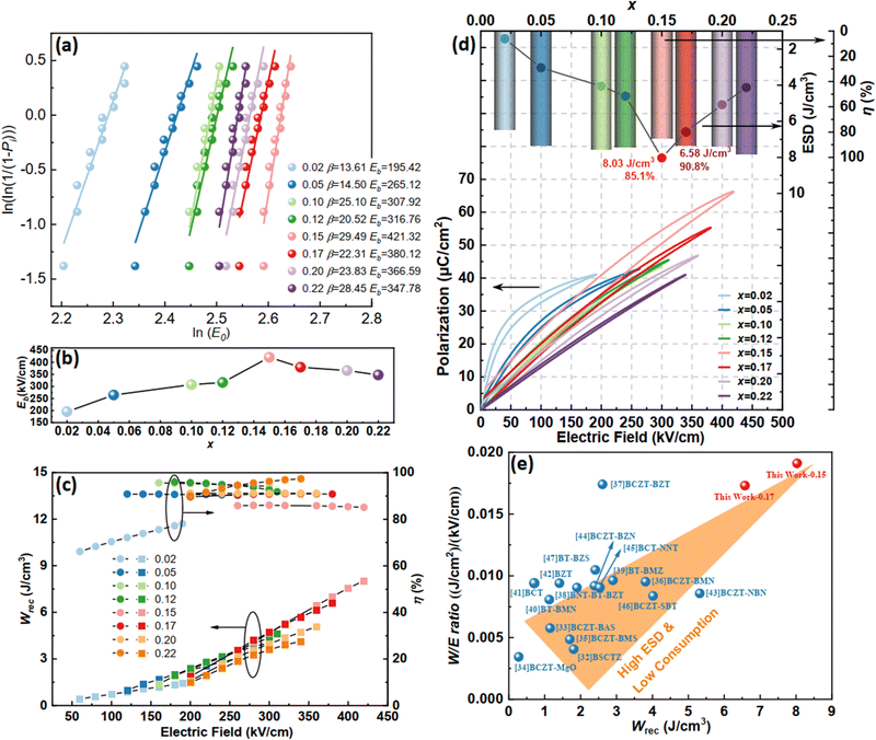 |
| | Fig. 2 (a) Weibull distribution; (b) the calculated Eb values of BCZT–xBZT with x = 0.02–0.22; (c) the calculated Wrec and η values of BCZT–xBZT with x = 0.02–0.22 under different electric fields; (d) unipolar P–E loops, Wrec, and η at Eb of BCZT–xBZT with x = 0.02–0.22; (e) comparison of the Wrec and W/E ratio of BCZT–xBZT with x = 0.15 and 0.17 in our work and those of some typical BZT-based ceramics.32–47 | |
3.3 Discussion of the polarization
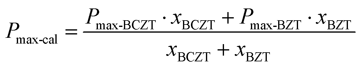
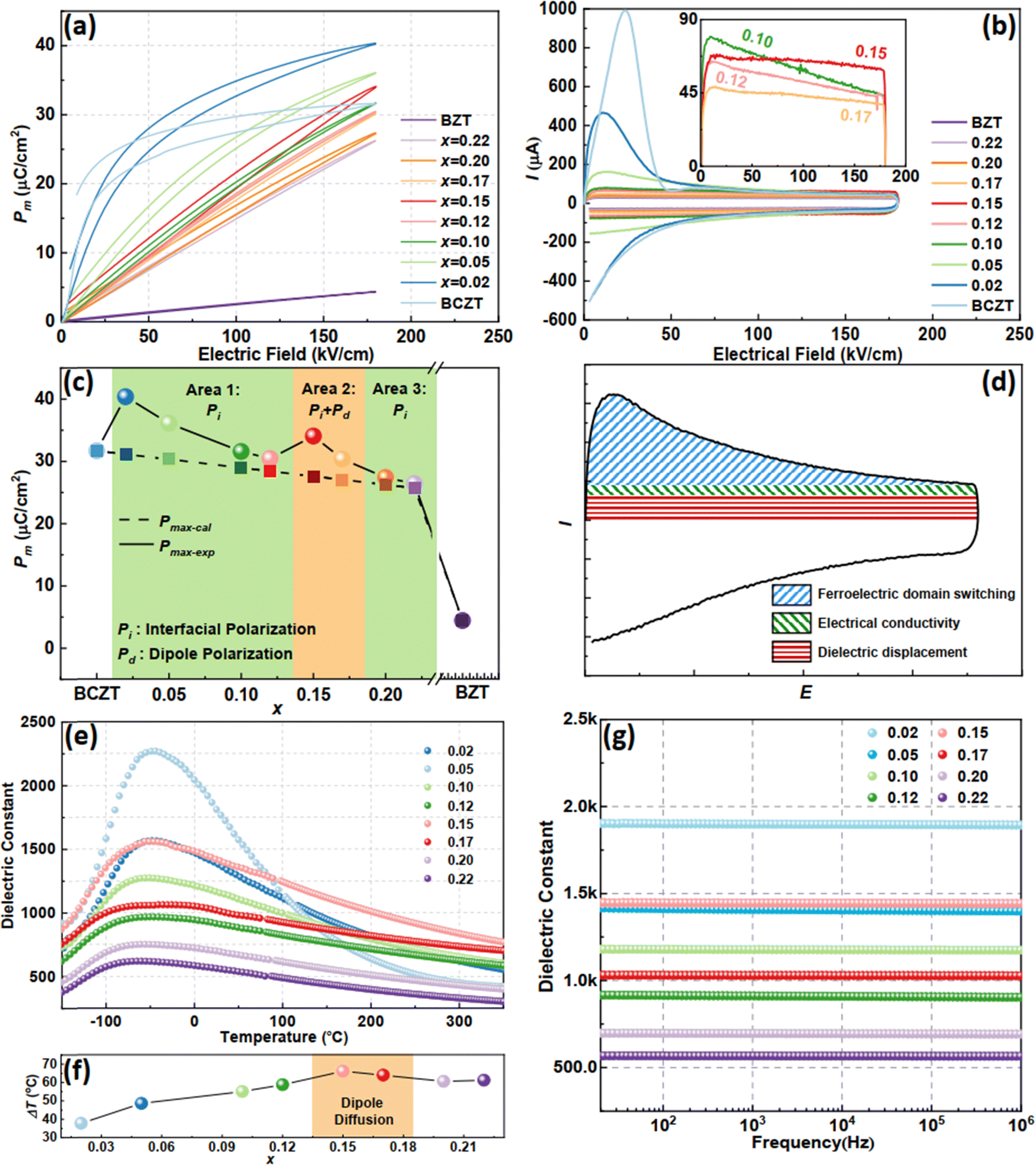
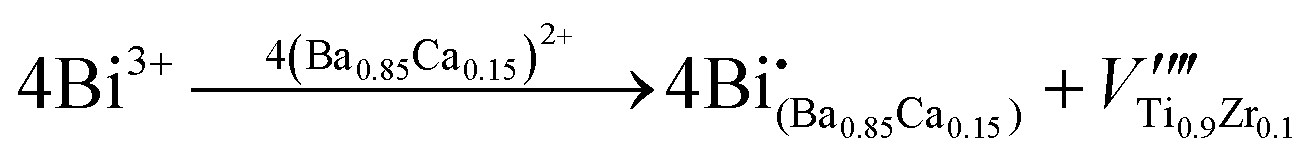
Fig. 3(a) displays the unipolar P–E loops of all the BCZT–xBZT ceramics with both pristine BCZT and BZT under the same electric field of 180 kV cm−1 and their corresponding polarization current–electric field (I–E) curves are shown in Fig. 3(b). Similar to most of the previous work, with increasing BZT content, the hysteresis of the loop weakens with decreasing Pmax, except for an abnormality around x = 0.15. To facilitate further analysis, we extracted the maximum polarization value in each loop as shown in Fig. 3(a), defined as Pmax-exp. We plotted the variation between Pmax-exp and x in Fig. 3(c). Meanwhile, utilizing the formula below| | 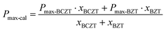 | (2) |
where Pmax-cal is the calculated value of Pmax, and Pmax-BCZT, Pmax-BZT, and xmax-BCZT, xmax-BZT is the maximum polarization of pristine BCZT, BZT, and the molar ratio of BCZT, BZT parts in each ceramic, respectively. The physical significance of this equation is very simple, just to see how much extra maximum polarization can be obtained by dissolving BZT into the BCZT lattice than the simple linear superposition according to the component of two ceramics. The relationship between Pmax-cal and x was also obtained and plotted in Fig. 3(c) for comparison. As is seen, Pmax-exp is higher than its counterparts when calculating in the whole x range. That is because all BCZT–xBZT is composed of two phases (the C-phase and the T-phase), as concluded from the results of the Rietveld XRD refinement; thus, the extra polarization in Pmax-exp should be caused by the interfacial polarization (Pi) between the two adjacent phases. Besides, two interesting phenomena also need to be analyzed: (1) the difference between Pmax-exp and Pmax-cal basically decreases with the increasing BZT content; (2) an abnormal increment occurs around x = 0.15 during such a difference's decrease. Eqn (S7)–(S12) in the ESI† explain the contribution of Pi to such a difference, so in the following part, we will focus on that abnormal increment. The decrement of the polarization current switching peak of the BCZT–xBZT ceramics, which signifies the coercive field (Ec) decrement, is also one of the typical phenomena for the FE-to-RFE transition, as seen in the I–E curves in Fig. 3(b). Interestingly, something new can be discovered when we enlarge the curves that fall into the x of the abnormal increment. As the inset in Fig. 3(b) shows, the I–E curves change gradually from a trapezoid to a rectangle from x = 0.10 to 0.17, and a current enhancement occurs at x = 0.15. This current enhancement is believed to be related to the abnormal increment between Pmax-exp and Pmax-cal. According to previous reports, the polarization current typically comprises three parts: ferroelectric domain switching, electrical conductivity, and dielectric displacement, as sketched in Fig. 3(d).50,51 Obviously, the contribution to the current of the domain switching decreases with increasing x, and meanwhile, the current enhancement at x = 0.15 is confirmed to be caused by the contribution of electrical conductivity. (The authors would like to say that though the BCZT–xBZT ceramics in this work are single-phase solid-solution rather than two-phased composites, it is still necessary to make a comparison between Pmax-cal and Pmax-exp. That is because the BCZT and BZT powders are synthesized separately, and the difference between the Pmax-cal and Pmax-exp is just the benefit of dissolving BZT into BCZT.)
 |
| | Fig. 3 (a) Unipolar P–E loops; (b) I–E curves of BCZT–xBZT with x = 0.02–0.22 at their Eb; (c) the variation of Pmax-cal and Pmax-exp with x; (d) sketch showing the contribution of different components to the polarization current in an I–E curve; (e) the ε–T curves of BCZT–xBZT with x = 0.02–0.22 at 1000 Hz from −50 °C to 350 °C; (f) the variation of ΔT of BCZT–xBZT with x; (g) the ε–f curves of BCZT–xBZT with x = 0.02–0.22 from 20–106 Hz at room temperature. | |
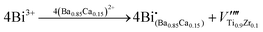
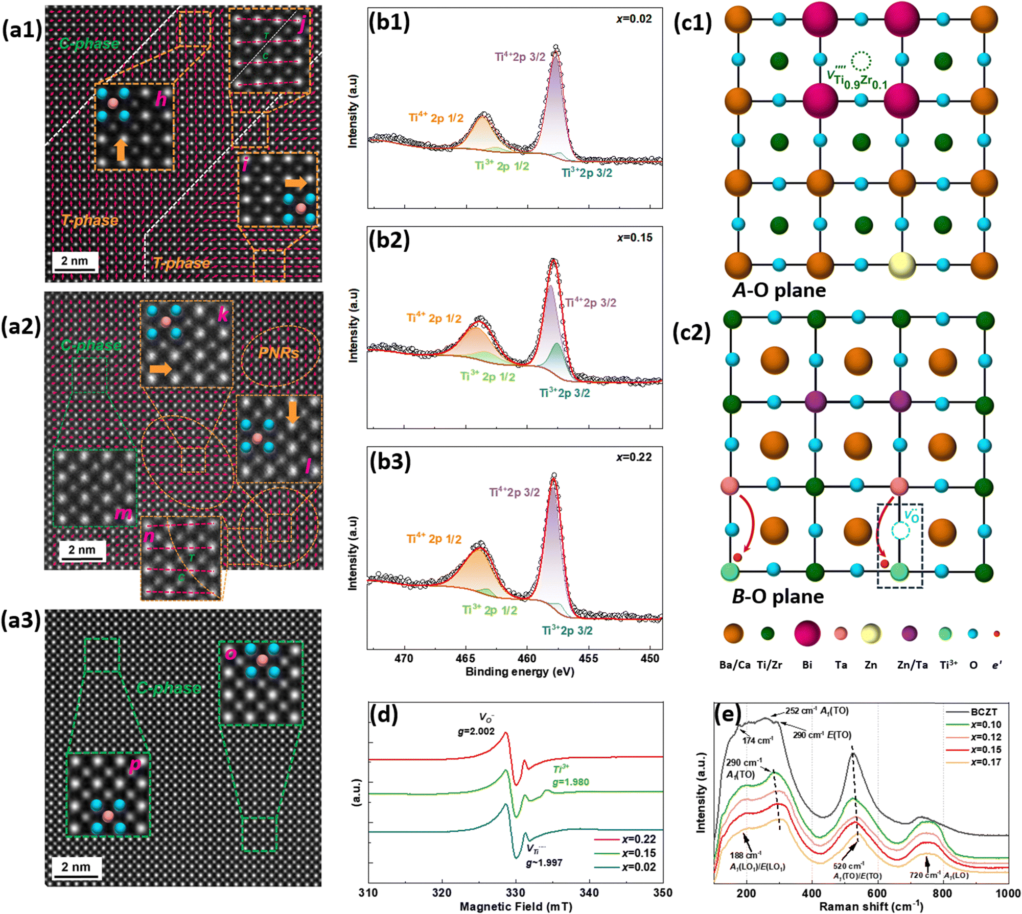
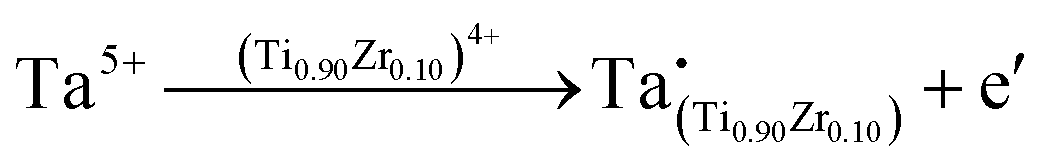
Fig. 4(a1) is the HAADF-STEM image of the BCZT–xBZT ceramic with x = 0.02 along the [100] crystal axis. According to the displacement of B-site atoms (weaker contrast for Ti/Zr/Zn/Ta) relative to the center of the four adjacent A-site atoms (stronger contrast for Ba/Ca/Bi), as displayed in illustration-h and illustration-i, the spontaneous polarization (Ps) orientation in the BCZT–xBZT ceramics’ lattice can be thus confirmed.52,53 As is seen, T-phase domains with an intersection angle of ∼90° are observed at the bottom right of the image, and the area on the top left corner shows a C-phase character. Illustration-j shows the microstructure of the interface between two phases, and the gradual change of lattice can be clearly detected. Instead of normal ferroelectric domains, only smaller-sized PNRs are observed in the HAADF-STEM image of BCZT–0.15BZT, as shown in Fig. 4(a2). Similarly, the spontaneous polarization (Ps) orientation of these PNRs can be determined by the displacement of the B-site atoms, as seen in illustration-k and illustration-l. Lattice distortion can also be observed in the interface between the C-phase and the PNR, as shown in illustration-n. We have mentioned above that the two-phase coexistence cannot be observed in BCZT–0.15BZT or BCZT–0.22BZT for the relatively low T-phase content. So, we transfer the HAADF image of BCZT–0.15BZT to the FFT image by employing Gwyddion, and the result is shown in Fig. S5(c) (ESI†). Each pattern in Fig. S5(c) (ESI†) is arranged neatly and separately, showing the characteristics of the single crystal. By enlarging the (02) and the (30) planes, which are circled in orange rectangles, both the C phase and the T phase can finally be detected. For BCZT–0.22BZT, only C-phase lattices exist, as seen in Fig. 4(a3). (There should be T-phase lattices in BCZT–0.22BZT, according to the Rietveld XRD refinement. However, due to the relatively low content and the resolution limitation of TEM, no T-phase was detected in this case.) According to such microstructure characterization, we can assume that over the entire x range, the amount of the T-phase lattice decreases with increasing BZT content, agreeing well with what we have concluded above. To find out the origin of the current enhancement in the I–E curves at x = 0.15, which is also considered the reason for the abnormal increment of the difference between Pmax-exp and Pmax-cal in Fig. 3(c), the X-ray photoelectron spectra (XPS) for Ti were obtained, and the results are illustrated in Fig. 4(b1)–(b3). Two peaks, which correspond to Ti 2p1/2 (∼463 eV) and Ti 2p3/2 (∼458 eV), can be detected for all the BCZT–xBZT ceramics with x = 0.02, 0.15, and 0.22. For all of them, after the Gaussian–Lorentz fitting, which was carried out with the assistance of the Origin software, every peak in each figure can be fitted into two, representing the existence of both Ti4+ and Ti3+ in their lattices. Compared to ceramics with x = 0.02 and 0.22, the Ti3+ peaks for BCZT–0.15BZT are much higher, which indicates a larger content of Ti3+, seemingly because the higher polarization in it is related to the formation of Ti3+. Then, defect chemistry was employed to explore the explanation. For BCZT–0.02BZT, as previous work reported, Bi and Zn/Ta occupied the A-site and B-site of the lattice, respectively, and it was a vacancy compensation mechanism. Thus, the related defect equations can be written as25
| |  | (3) |
| |  | (4) |
 |
| | Fig. 4 (a1)–(a3) The HAADF images; (b1)–(b3) the XPS spectrum; (d) the EPR spectrum of BCZT–xBZT with x = 0.02, 0.15, and 0.22; sketch of the lattice of (c1) A–O plane and (c2) B–O plane explaining eqn (5)–(9); (e) Raman spectra of BCZT, and BCZT–xBZT with x = 0.10, 0.12, 0.15 and 0.17 at room temperature. | |
When the BZT doping content is increased to 0.15, because the Zn/Ta's substitution causes a lattice expansion, as seen in Fig. S1(b2) (ESI†), a small amount of Zn2+ will occupy the A-site, leaving Ta5+ in the B-site. Many previous studies also confirm the possibility of Zn2+ entering into the A-site of ABO3 perovskites,54–56 offering credibility to our assumption. In this case, along with the vacancy compensation mechanism, the electron defect compensation mechanism occurs at the same time, which can be expressed using the defect equations as follows:
| |  | (5) |
| |  | (6) |
| |  | (7) |
| |  | (8) |
Fig. 4(c1) sketches the lattice of the
A–
O plane in the BCZT–0.15BZT lattice and shows the defect reactions in
eqn (5) and (7), and
Fig. 4(c2) sketches the
B–
O plane with the defect reactions in
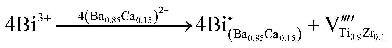
eqn (6), (8) and (9). For the higher dopant ceramic of BCZT–0.22BZT, further lattice expansion occurs, which gives the chance of A-site occupation for both Zn
2+ and Ta
5+, and the defect reaction will be changed to
| |  | (10) |
| |  | (11) |
| |  | (12) |
The complete form of these equations is provided in the ESI.
† The lattice sketches for both the
A–O and
B–O planes of all these three are shown in Fig. S8 (ESI
†). Up to now, it can be confirmed that the abnormal increase in
Pmax-exp of BCZT–0.15BZT is caused by the existence of the newly formed dipoles

, and such a defect dipole is circled in a black dashed rectangle in
Fig. 4(c2). In this case,
Fig. 3(c) can be separated into three areas: the polarization differences in area-1 and area-3 are both attributed to
Pi, while that in area-2 is caused by the combined effect of
Pi and dipole polarization (
Pd), which can be defined as a polarization double-enhancement. Such an effect enables higher
Wrec to be triggered by a lower external electric field, giving the low-consumption character to the BCZT–0.15BZT ceramic. Another proof for such defect equations comes from the electron paramagnetic resonance (EPR) measurement, as seen in
Fig. 4(d). The
g factor in the spectra is calculated according to
eqn (13),
| |  | (13) |
in which
h,
μB,
ν, and
B are the Planck constant, Bohr magneton, applied microwave frequency, and the resonance magnetic field, respectively. A symmetrical peak around
g ∼ 2.002 can be detected in the spectra of all the ceramics, which proves the existence of

.
57,58 The peak for
g ∼ 2.002 comes from

, according to some latest works.
59,60 As expected, a signal for Ti
3+ is seen in the spectra of BCZT–0.15BZT, and the assumption above for
eqn (5)–(9) can be thus confirmed.
61 In general, for ceramics sintered at high temperatures, the reduction reaction of the Ti
4+–Ti
3+ transition occurs very often. But because the amount of Ti
3+ coming from such a reaction is so tiny that the EPR test in our work cannot recognize it, the peak at
g ∼ 1.980, symbolized for the Ti
3+, only exists in BCZT–0.15BZT. The variations of defect equations with BZT doping content can also be confirmed by the Raman spectra, shown in
Fig. 4(e). The spectrum of pure BCZT, which is measured as a control group in this work, is similar to that of a typical BaTiO
3 ceramic, which is distinguished by the antiresonant dip at ∼174 cm
−1, an A
1 (TO) mode at ∼252 cm
−1, and an E (TO) mode at ∼290 cm
−1. For BCZT–
xBZT with
x being 0.10 to 0.17: (1) the wavenumber region below 200 cm
−1 symbolizes the cation vibration of the A-site atoms, while the region from 200 to 450 cm
−1 is caused by the bond vibration between B-site atoms O; (2) the wavenumber region from 450 to 650 cm
−1 is correlated with the BO
6 octahedra.
62,63 The peak around 188 cm
−1 becomes more and more diffused with increasing
x. The peak around 290 cm
−1, however, becomes diffused when
x is increased from 0.10 to 0.12, and further
x increments have no obvious effect on it. Peak diffusion is strongly related to the disorder of the lattice; such a phenomenon indicates that small doping of BZT affects both the A-site and the B-site, while extra doping only has more effect on the A-site. At this time, it is necessary for us to take a short look at the dielectric behavior of the BCZT–
xBZT ceramics. Fig. S9 (ESI
†) displays the temperature dependence of dielectric constant (
ε–
T curve) and dielectric loss (tan
δ–
T curve) of all these ceramics from −150 °C to 350
°C at different frequencies, and the curve at 1000 Hz of each component is summarized in
Fig. 3(e). The phase transition peak is located at ∼−50 °C for all the ceramics, and with increase of
x, the peak fades but broadens, indicating an increment of dielectric thermal stability. The difference of the temperature at the highest
ε value from 1 kHz to 1 MHz (Δ
T) of the ceramic with different
x values is summarized in
Fig. 3(f), and the Δ
T increases with increasing
x with a maximum value of Δ
T = 66 °C at
x = 0.15. Δ
T is strongly related to the relaxor behavior of the RFE, and such a good behavior of BCZT–0.15BZT is due to the extra types of defects mentioned above.
Fig. 3(g) plots the frequency dependence of
ε (
ε–
f curve), and tan
![[thin space (1/6-em)]](https://www.rsc.org/images/entities/i_char_2009.gif) δ
δ (tan
δ–
f curve) of all these ceramics from 20 Hz to 10
6 Hz, and all the ceramics show excellent dielectric frequency stability in such a range.
3.4 Discussion of the electric breakdown strength
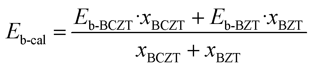
Similar to how we analyze the polarization, we also compare the Eb experimental value (Eb-exp) and the calculated value (Eb-cal) in Fig. 5(a), and the latter was obtained according to the following equation:| |  | (14) |
Eb-BCZT and Eb-BZT are the electric breakdown strength of the pristine BCZT and BZT ceramics, respectively. Eb-exp, which increases firstly and then decreases with increasing x, is higher than Eb-cal, which increases monotonously with increasing x, for all the BCZT–xBZT ceramics. Such a result can be rationalized as follows: compared to the T-phase, the C-phase has smaller B-site atom displacement and thus higher voltage endurance, and Eb-cal increases with increasing x, consistent with our previous conclusions.4 The extra voltage endurance in Eb-exp probably comes from the blocking behavior of the electric current spread of the interfacial area between the T-phase and the C-phase. A similar behavior has already been explored by enormous work based on both experiments and computing simulations. Though the detailed mechanism of such a blocking behavior is not fully understood, it can be attributed to the space charges induced by the lattice distortion in the interface between two phases, as discussed above.64–68 Thus, in this work, the author will focus more on a newly discovered phenomenon. Based on the Eb-exp's variation with x, an unexpected Eb enhancement from x = 0.15–0.17 is seen, and to understand this, we fit such a variation by kicking out the data of x = 0.15–0.17 by the polynomial fit function in the Origin software and the result is shown as the red line in Fig. 5(a). Obviously, Eb-exp has a significant deviation from the fitting result, which tells us that there should be another factor that affects the generation of such an Eb enhancement. Considering the generation of extra electrons as expressed in eqn (8), we took the current density (J)–electric field (E) measurements on the BCZT–xBZT ceramics with x = 0.12–0.17, and such curves are plotted in Fig. 5(b1). As expected, BCZT–0.15BZT has a higher J than the other two. To deeply understand their conductive mechanism, we fit the J–E curves according to the Poole–Frenkel (P–F) mode, Fowler–Nordheim (F–N) tunneling mode, ohmic conduction mode, space charge limited current (SCLC) mode and Schottky emission mode, respectively,69 and found that the Schottky emission mode, which can be expressed as follows:| | 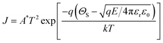 | (15) |
occurs in the higher electric field strength range of BCZT–0.15BZT, as seen in Fig. 5(b2). J, ΦS, E, and T are the current density, Schottky barrier potential, electric field across the material, and absolute temperature, respectively. A*, k, q, ε0, and εr, which would not change with external factors, are the effective Richardson constant, Boltzmann's constant, electronic charge, vacuum dielectric constant, and relative dielectric constant, respectively.69 In such a fitting result, the Schottky emission mode is proved by the linear relationship between logJ and E1/2. (By comparing the relative dielectric constant determined from the linear slope with the value measured at the optical frequency, the validity of this model can be verified, as reported in our previous work.70,71) Our ceramics have a symmetric structure with the Au electrodes on both sides; in general, discussing only one-side interface between the ceramic and electrode is enough. Fig. 5(c1) is the schematic illustration of one such interface under the external voltage (V) pointing from right to left, and a depletion region (Rd), which has the same orientation, should exist. To show a clear physical picture behind such a linear relationship, the band diagram of the Au/BCZT–0.15BZT interface in this electric field range is illustrated in Fig. 5(c2). Owing to the electron compensation type defect equation of BCZT–0.15BZT, as mentioned in eqn (8), a depletion region (Rd) was formed at the Au/BCZT–0.15BZT interface, which shows a blocking behavior to the electron spread. To prove such a behavior, we deleted the linear area in the logJ–E1/2 relationship of BCZT–0.15BZT in Fig. 5(b2) and then extended the data according to its remaining part under the assistance of the Origin software, and the result is plotted as a dashed line. Compared to the experimental curve, the fitted one shows higher current density in a higher electric field range, indicating that the formation of a built-in potential indeed blocks the current spread. More details of the formation of such a Schottky barrier are shown in Fig. S10(a)–(c) (ESI†). Fig. 5(c3) shows the band diagram of the interface between Au electrodes and BCZT–xBZT with x = 0.12 or 0.17. During a breakdown process, a typical dielectric material can be composed of an insulator layer (LI) and a conductor layer (LC) connected in series; once LI is broken down, the whole material will be destroyed soon.72 In addition to the above, we still obtained the bipolar P–E loop at 260 kV cm−1 of BCZT–xBZT with x = 0.12, 0.15, and 0.17, respectively. These loops are taken in the first voltage cycle after a long time. As illustrated in Fig. S7(c) (ESI†), the loops of BCZT–xBZT with x = 0.12 and 0.17 are symmetric around zero, while that of BCZT–0.15BZT has an opening in the negative side, showing quasi-diode properties. This is also a piece of evidence to prove the existence of the built-in potential in the Au/ceramic interface in BCZT–0.15BZT. Once the negative voltage was applied, the trapped electrons were released in the ceramic, leading to a higher electronic conductivity and a broader loop.
 |
| | Fig. 5 (a) The variation of Eb-cal and Eb-exp with x; the relationship between (b1) logJ and E; (b2) logJ and E1/2 of BCZT–xBZT with x = 0.12, 0.15, and 0.17; (c1) the schematic illustration of the interface between the Au electrode and BCZT–0.15BZT; (c2) band diagram showing the formation of the built-in potential of BCZT–0.15BZT in a high electric field range in the logJ–E1/2 relationship of x = 0.15; (c3) the band diagram of the interface between Au electrodes and BCZT–xBZT with x = 0.12 or 0.17; the spread of the current density of (d1) BCZT–0.02BZT; (d2) BCZT–0.15BZT; and (d3) BCZT–0.22BZT at 400 kV cm−1 simulated using COMSOL Multiphysics 6.0. | |
To visually observe the electric breakdown process, computer simulation was applied using the finite element method through the COMSOL Multiphysics6.0 linking with Matlab5.2. Fig. 5(d1)–(d3) depict the current density distribution of the BCZT–xBZT ceramic with x = 0.02, 0.15, and 0.22 under 400 kV cm−1, respectively. The small polygons in each ceramic represent the ferroelectric domain, and the ones marked with “T” are the T-phase, while the rest are the C-phase. Based on the microstructure characterization above, compared to BCZT–0.02BZT, the number of the T-phase domain in BCZT–0.15BZT decreases, and the domain size also becomes smaller, and no T-phase exists in BCZT–0.22BZT. The physical model of such a simulation is explained in the ESI.† From these results, we can see that despite being broken down, the interfaces between the T-phase and C-phase in BCZT–0.02BZT show a blocking behavior to the current. As expected, BCZT–0.22BZT was also broken down under the same electric field. By adding a Schottky contact, no breakdown occurs in BCZT–0.15BZT, which agrees well with the experimental results. The distributions of electric potential and electric field of these ceramics are displayed in Fig. S11(a1)–(a3) and (b1)–(b3) (ESI†), respectively. A video was also provided separately in the ESI† to show the breakdown process.
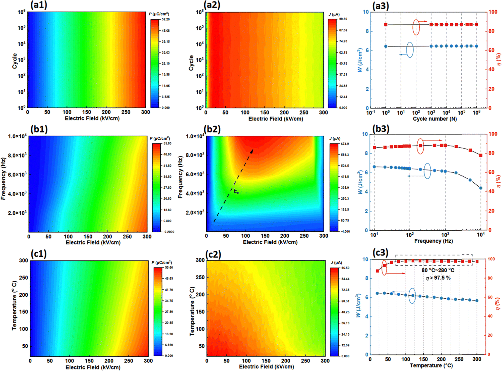
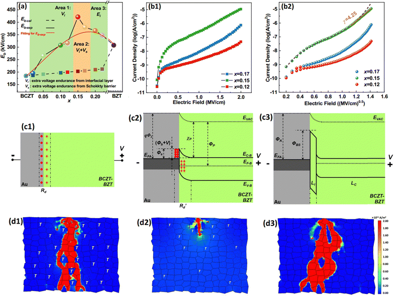
3.5 Characterization of the energy storage reliability
Fig. S12(a) and (b) (ESI†) show the unipolar P–E loops and I–E curves of the BCZT–0.15BZT ceramic obtained during polarization fatigue from the 1st to 106th cycle under 300 kV cm−1, respectively. The variation of polarization and polarization current with both the electric field and cycling number during voltage ramping up steps are summarized in maps displayed in Fig. 6(a1) and (a2), respectively. Excellent polarization fatigue endurance is achieved by almost no change in both polarization and current observed. The energy storage performance of the BCZT–0.15BZT ceramic during such a process is summarized in Fig. 6(a3), and the decrement in Wrec and η is only 0.5% and 0.9%, respectively. Fig. S13(a) and (b) (ESI†) show unipolar P–E loops and I–E curves of the BCZT–0.15BZT ceramic measured from 10 Hz to 10000 Hz under 300 kV cm−1 at room temperature, respectively. The maps of the polarization and polarization current variations with both the electric field and frequency during voltage ramping up are displayed in Fig. 6(b1) and (b2), respectively. Oblique stripes can be seen in Fig. 6(b1), which indicates that loops measured under higher frequencies increase more slowly and have lower polarization than those measured under lower frequencies, and that is because some relaxor polarizations cannot keep up with the external field switching, and thus do not contribute to the total polarization of the ceramic.73,74 The map in Fig. 6(b2) tells us that the polarization current increases with increasing frequency and indicates that Ec has the same tendency, as marked with a black dashed arrow. For the first phenomenon, according to the discussion in Fig. 3(b), the higher current in the I–E curves measured under higher frequencies should come from the dielectric displacement for the dipole polarization, which is considered as the origin of the electrical conductivity and it would not contribute to the polarization under such high frequencies. Based on the mathematical derivation in R. Meyer et al.'s work, the dielectric displacement is proportional to the frequency, which agrees well with our result.75 The second phenomenon is related to the domain (or PNR) switching behavior, as Z. Chen et al. have reported. Due to the different spontaneous polarization directions of the PNRs in BCZT–0.15BZT, the dielectric displacement relaxor switching behavior can be thus observed.76Fig. 6(b3) shows the energy storage performance of the BCZT–0.15BZT ceramic in such a frequency range; a decrement of 33.8% and 11.8% was observed for Wrec and η, respectively. Fig. S14(a) and (b) (ESI†) plot the unipolar P–E loops and I–E curves of BCZT–0.15BZT measured from 25 °C to 150 °C at 300 kV cm−1, and a map of polarization and current variations with the electric field and temperature during the voltage ramping up is displayed in Fig. 6(c1) and (c2), respectively. With increasing temperature, the polarization decreases, and the variation between the polarization current and the electric field becomes flat. These results can be easily understood from the ε–T curve of BCZT–0.15BZT, which illustrates the FE–RFE phase transition during such a temperature range. Fig. 6(c3) shows the energy storage performance of the BCZT–0.15BZT ceramic during such a temperature range. With increasing temperature, Wrec decreases slightly from 6.45 J cm−3 to 5.64 J cm−3, while η increases to nearly 100% over 800 °C and is retained for quite a broad temperature range from 80 °C to 250 °C, as shown by a black dashed rectangle in Fig. 6(c3). According to one of the latest reports, one reason for such a near-zero energy loss behavior is the existence of a multiphase heterostructure.77η decrement at higher temperatures over 250 °C should be caused by more activated TaTi–Ti3+ dipoles.78,79
 |
| | Fig. 6 Mapping of the variation of (a1) polarization; (a2) polarization current density with electric field and cycle number; and (a3) variation of Wrec and η with cycle number from 1st to 106th at room temperature of BCZT–0.15BZT. Mapping of the variation of (b1) polarization; (b2) polarization current density with electric field and frequency; and (b3) variation of Wrec and η with frequency from 10 Hz to 10000 Hz at room temperature of BCZT–0.15BZT. Mapping of the variation of (c1) polarization; (c2) polarization current density with electric field and temperature; and (c3) variation of Wrec and η with temperature from 25 °C to 300 °C of BCZT–0.15BZT. | |
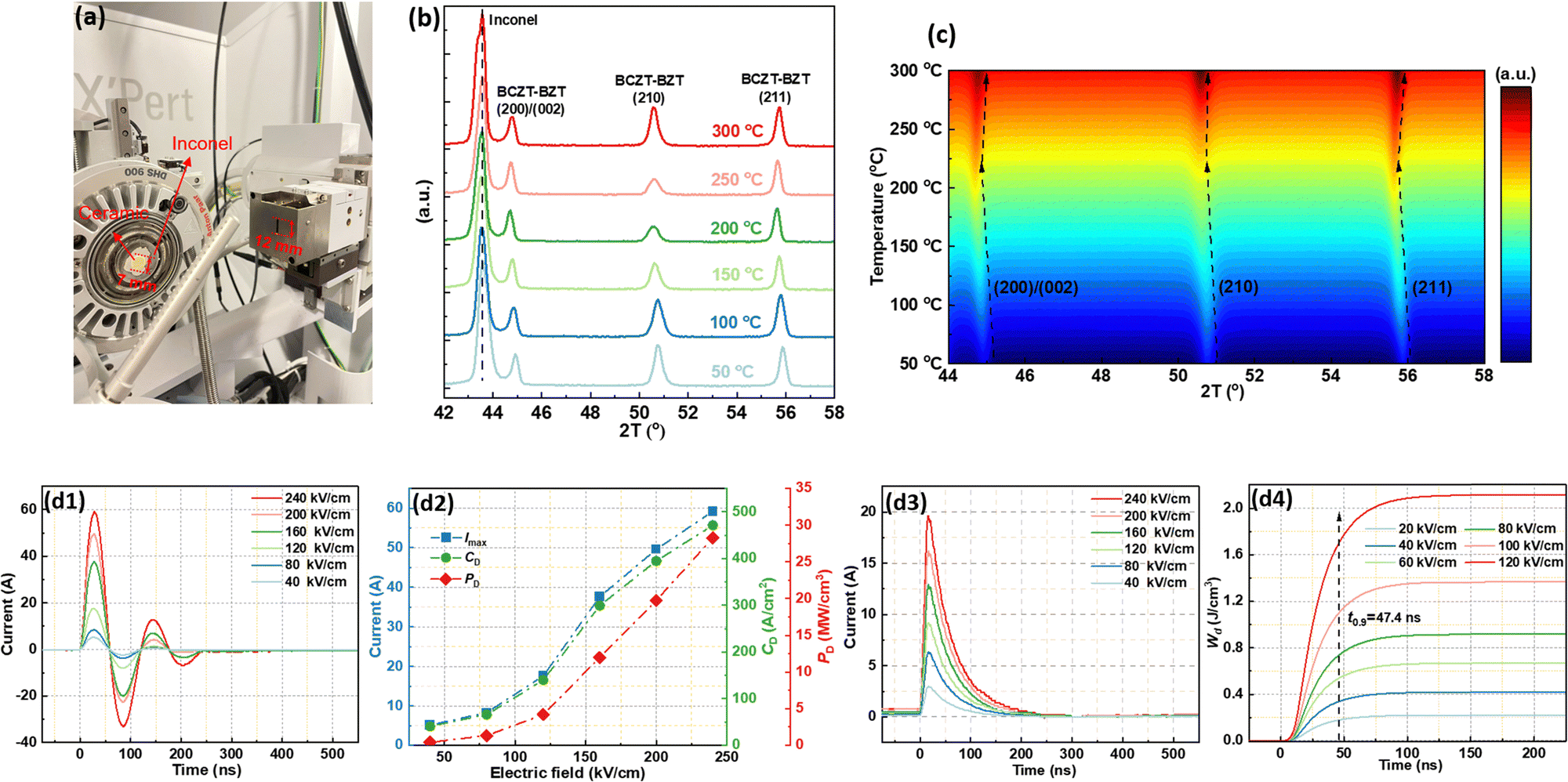
Afterward, we carried out high-temperature XRD (HT-XRD) measurements on BCZT–0.15BZT to find out more information on its structure transformation during temperature increment. Fig. 7(a) is the picture of the high-temperature stage of the HT-XRD system. Because the slit of the X-ray beam is longer than the ceramic diameter, the data for such an experiment inevitably involve the X-ray diffraction signal of the Inconel stage. Fig. S15 (ESI†) displays the XRD scan of BCZT–0.15BZT from the diffraction angle of 20° to 120° in the temperature range from 50 °C to 300 °C. The enlarged view from 42° to 58° is shown in Fig. 7(b). Three diffraction peaks, which represent the (200)/(002), (210), and (211) planes with one peak for the Inconel stage, are observed. To reveal the temperature evolution of the BCZT–0.15BZT structure, the peak intensity variation with both the diffraction 2θ angle and temperature is summarized in the mapping displayed in Fig. 7(c). All three peaks shift to a lower angle from 50 °C to 225 °C and back from 225 °C to 300 °C. That is probably because of the lattice expansion with the T-phase content decrement and the C-phase content increment in 50–225 °C, and then the lattice shrinking when the T-phase is completely changed to the C-phase. As we mentioned above, such a near-zero energy loss behavior is due to the existence of a multiphase heterostructure, according to one of the latest reports.77 At the same time, in the authors’ opinion, another reason should also be considered. The lattice expansion of the BCZT–0.15BZT ceramic increases its entropy during the temperature range from 50 °C to 225 °C, and the higher entropy characteristics in ferroelectrics always lead to the slimming of P–E loops, because of the local polymorphic distortion or structural fluctuation.80–83
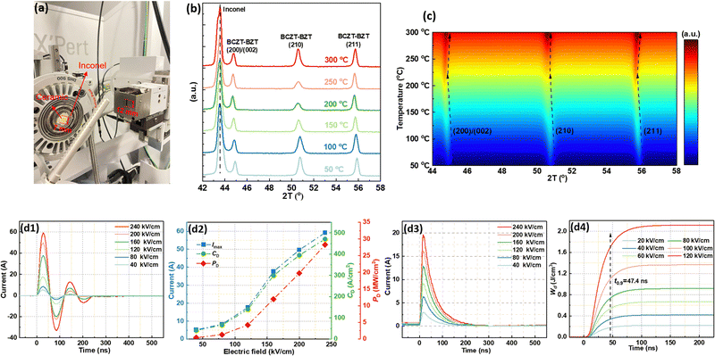 |
| | Fig. 7 (a) Photograph showing the HT-XRD measurement; (b) HT-XRD scans of BCZT–0.15BZT from 42° to 58° in the temperature range from 50 °C to 300 °C; (c) mapping of peak intensity variation with both the diffraction 2θ angle and temperature; (d1) underdamped; (d2) Imax, CD, and PD; (d3) overdamped discharge current waveforms; and (d4) Wd depending on time of BCZT–0.15BZT under different electric fields. | |
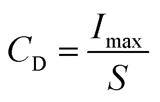
Using a pulsed charge–discharge test, the practical application performance of the BCZT–0.15BZT as a capacitor in terms of energy storage is evaluated. Fig. 7(d1) shows the underdamped discharge curves of BCZT–0.15BZT, which are obtained using an R–L–C circuit under different electric fields. A similar discharge behavior was observed under various electric fields, and the first current's peak value increases with an increasing electric field. The variation of maximum current (Imax), current density (CD), and power density (PD) with the electric field, as plotted in Fig. 7(d2), increases monotonously with the electric field, according to the formulas below:
| |  | (16) |
| |  | (17) |
The values of
Imax,
CD, and
PD reach the maximum of 59.5 A, 472.6 A cm
−2, and 28.4 MW cm
−3 at 240 kV cm
−1, respectively.
Fig. 7(d3) shows the overdamped pulse discharge current under different electric fields with a load resistance (
RL) of 100 Ω, and a similar tendency of the variation of the peak current with electric field was obtained. Using the formula below,
| |  | (18) |
the time dependence of the discharge energy density (
WD) was calculated and plotted in
Fig. 7(d4).
R,
V,
I, and
t in
eqn (16) are the load resistance, sample volume, discharge current, and time, respectively. As a result, a
WD of 2.12 J cm
−3 at 240 kV cm
−1 with a
t0.9, which means the time required for dielectric capacitors to release 90% of the total energy stored, of 47.4
ns, was obtained.
WD is lower than the value obtained from the static method, which is calculated to be ∼3.00 J cm
−3, as inferred from
Fig. 2(c). This is due to the clamping effect on the ferroelectric domains, which has been reported frequently elsewhere.
2 Such a result indicates that the BCZT–0.15BZT ceramic is a promising candidate for pulsed power capacitor applications.
4. Conclusions
Polarization double-enhancement, which is composed of the interfacial polarization and the dipole polarization, was achieved by incorporating BZT into the BCZT lattice, and an ultrahigh ferroelectric polarization was achieved at a BZT content of 0.15. Combining this with the Schottky emission-modified Eb, a Wrec value of 8.03 J cm−3, the highest among the BCZT-based ceramics, with extremely low energy consumption, was finally obtained. The defect equation, band theory, and the finite element simulations were employed to verify the credibility of our work. As for the reliability, BCZT–0.15BZT has rather good polarization fatigue, energy storage frequency and thermal stability, and a near-zero energy loss behavior was even observed in the temperature range from 80 °C to 280 °C. Good discharge properties were also observed. Our work proposed an ingenious way to successfully solve one of the critical paradoxes in energy storage capacitors and provided an important theoretical basis for designing the next-generation functional devices.
Author contributions
Zixiong Sun: conceptualization, methodology, writing – reviewing and editing, supervision, and funding acquisition; Yuhan Bai: data curation; Hongmei Jing: writing – reviewing and editing; Tianyi Hu: data curation; Qing Guo: data curation; Pan Gao: writing – reviewing and editing; Chunrui Ma: writing – reviewing and editing; Ming Liu: supervision; and Yongping Pu: funding acquisition and supervision.
Conflicts of interest
The authors declared that they have no conflicts of interest in this work.
Acknowledgements
This work was financed by the National Natural Science Foundation of China (52002234), the Open Foundation of Hubei Key Laboratory of Micro-Nanoelectronic Materials and Devices (K202313), the Open Foundation of Key Laboratory of Auxiliary Chemistry and Technology for Chemical Industry, Ministry of Education, Shaanxi University of Science and Technology (no. KFKT2021-09), and the Shaanxi Collaborative Innovation Center of Industrial Auxiliary Chemistry and Technology, Shaanxi University of Science and Technology (no. KFKT2021-09).
References
- Y. Zhang, L. Chen, H. Liu, S. Deng, H. Qi and J. Chen, InfoMat, 2023, e12488 CrossRef CAS.
- L. Yang, X. Kong, F. Li, H. Hao, Z. Cheng, H. Liu, J.-F. Li and S. Zhang, Prog. Mater. Sci., 2019, 102, 72 CrossRef CAS.
- X. Wang, F. Yang, K. Yu, B. Zhang, J. Chen, Y. Shi, P. Yang, L. He, H. Li and R. Liu, Adv. Mater. Technol., 2023, 2202044 CrossRef CAS.
- Z. Sun, Y. Bai, J. Liu, G. Jian, C. Guo, L. Zhang and Y. Pu, J. Alloys Compd., 2022, 909, 164735 CrossRef CAS.
- X. Fan, J. Wang, H. Yuan, Z. Zheng, J. Zhang and K. Zhu, J. Adv. Ceram., 2023, 12, 649 CrossRef CAS.
- X. Wang, Y. Lu, P. Li, J. Du, P. Fu, J. Hao and W. Li, Inorg. Chem., 2024, 63(15), 7080–7088 CrossRef CAS PubMed.
- Z. Sun, S. Wang, S. Zhao, H. Wei, G. Shen, Y. Pu and S. Zhang, J. Mater. Chem. C, 2024, 12(3), 859–867 RSC.
- Q. Li, F.-Z. Yao, Y. Liu, G. Zhang, H. Wang and Q. Wang, Annu. Rev. Mater. Sci., 2018, 48, 219 CrossRef CAS.
- Z. Sun, Z. Wang, Y. Tian, G. Wang, W. Wang, M. Yang, X. Wang, F. Zhang and Y. Pu, Adv. Electron. Mater., 2020, 6, 1900698 CrossRef CAS.
- M. Guo, J. Jiang, Z. Shen, Y. Lin, C.-W. Nan and Y. Shen, Mater. Today, 2019, 29, 49 CrossRef CAS.
- X. Zhang, J. Jiang, Z. Shen, Z. Dan, M. Li, Y. Lin, C.-W. Nan, L. Chen and Y. Shen, Adv. Mater., 2018, 30, 1707269 CrossRef PubMed.
- Z. Sun, S. Huang, W. Zhu, Y. A. Brikholizer, X. Gao, R. A. Avila, H. Huang, X. Luo, E. P. Houwman, M. D. Nguyen, G. Koster and G. Rijnders, APL Mater., 2023, 101129 CrossRef CAS.
- M. Yang, W. Ren, M. Guo and Y. Shen, Small, 2022, 18, 2205247 CrossRef CAS PubMed.
- M. Zhang, B. Zhu, X. Zhang, Z. Liu, X. Wei and Z. Zhang, Mater. Horiz., 2023, 10, 2455 RSC.
- M. Feng, Y. Feng, C. Zhang, T. Zhang, Q. Chen and Q. Chi, Mater. Horiz., 2022, 9, 3002 RSC.
- B. Chu, J. Hao, P. Li, Y. Li, W. Li, L. Zheng and H. Zeng, ACS Appl. Mater. Interfaces, 2022, 14, 19683 CrossRef CAS PubMed.
- D. Li, D. Zhou, D. Wang, W. Zhao, Y. Guo and Z. Shi, Adv. Funct. Mater., 2022, 32, 2111776 CrossRef CAS.
- X. Wang, X. Wang, Y. Huan, C. Li, J. Ouyang and T. Wei, ACS Appl. Mater. Interfaces, 2022, 14, 9330 CrossRef CAS PubMed.
- W. Li, J. Shi, K. H. L. Zhang and J. L. MacManus-Driscoll, Mater. Horiz., 2020, 7, 2832 RSC.
- W. Pan, M. Cao, H. Hao, Z. Yao, Z. Yu and H. Liu, J. Eur. Ceram. Soc., 2020, 40, 49 CrossRef CAS.
- Y. Meng, K. Liu, X. Zhang, X. Lei, J. Chen, Z. Yang, B. Peng, C. Long, L. Liu and C. Li, J. Am. Ceram. Soc., 2022, 105, 5725 CrossRef CAS.
- J. Lin, G. Ge, K. Zhu, H. Bai, B. Sa, F. Yan, G. Li, C. Shi, J. Zhai and X. Wu, Chem. Eng. J., 2022, 444, 136538 CrossRef CAS.
- Y. Sun, L. Zhang, Q. Huang, Z. Chen, D. Wang, M. M. Seyfouri, S. L. Y. Chang, Y. Wang, Q. Zhang, X. Liao, S. Li, S. Zhang and D. Wang, Adv. Sci., 2022, 9, 2203926 CrossRef CAS PubMed.
- Z. Chen, X. Bu, B. Ruan, J. Du, P. Zheng, L. Li, F. Wen, W. Bai, W. Wu and Y. Zhang, J. Eur. Ceram. Soc., 2020, 40, 5450–5457 CrossRef CAS.
- C. Wang, H. Li, Q. Zhang, J. Zhao, R. Muhammad, D. Han and D. Wang, J. Eur. Ceram. Soc., 2023, 43, 6844 CrossRef CAS.
- D. Zhang, D. Sando, P. Sharma, X. Cheng, F. Ji, V. Govinden, M. Weyland, V. Nagarajan and J. Seidel, Nat. Commun., 2020, 11, 349 CrossRef CAS PubMed.
- Y. Ning, Y. Pu, C. Wu, S. Zhou, L. Zhang, J. Zhang, X. Zhang and Y. Shang, J. Mater. Sci. Technol., 2023, 145, 66 CrossRef CAS.
- W. Wang, L. Zhang, R. Jing, Q. Hu, D. O. Alikin, V. Ya. Shur, X. Wei, G. Liu, Y. Yan and L. Jin, Chem. Eng. J., 2022, 434, 134678 CrossRef CAS.
- W. Wang, L. Zhang, Y. Yang, W. Shi, Y. Huang, D. O. Alikin, V. Y. Shur, Z. Luo, A. Zhang, X. Wei, D. Wang, F. Gao, H. Du and L. Jin, J. Mater. Chem. A, 2023, 11, 2641 RSC.
- R. Lu, Z. Shen, C. Ma, T. Duan, L. Lu, G. Hu, T.-Y. Hu, C. You, S. Mi and C.-L. Jia, J. Mater. Chem. A, 2022, 10, 17166 RSC.
- T.-Y. Hu, C. Ma, J. Fan, Y. Wu, M. Liu, G. Hu, C. Ma and C.-L. Jia, Nano Energy, 2022, 98, 107313 CrossRef CAS.
- D. Li, D. Zhou, D. Wang, W. Zhao, Y. Guo, Z. Shi, T. Zhou, S.-K. Sun, C. Singh and S. Trukhanov, Small, 2023, 19, 2206958 CrossRef CAS PubMed.
- Y. Li, Y. Liu, M. Tang, J. Lv, F. Chen, Q. Li, Y. Yan, F. Wu, L. Jin and G. Liu, Chem. Eng. J., 2021, 419, 129673 CrossRef CAS.
- A. Jain, Y. Wang, N. Wang and F. Wang, Ceram. Int., 2020, 46, 28800 CrossRef.
- H. Yang, F. Yan, G. Zhang, Y. Lin and F. Wang, J. Alloys Compd., 2017, 720, 116 CrossRef CAS.
- K. Xu, P. Yang, W. Peng and L. Li, J. Alloys Compd., 2020, 829, 116 Search PubMed.
- D. Han, C. Wang, Z. Zeng, X. Wei, P. Wang, Q. Liu, D. Wang and F. Meng, J. Alloys Compd., 2020, 902, 163721 CrossRef.
- Z. Dai, J. Xie, Z. Chen, S. Zhou, J. Liu, W. Liu, Z. Xi and X. Ren, Chem. Eng. J., 2021, 410, 128341 CrossRef CAS.
- A. R. Jayakrishnan, P. V. K. Yadav, J. P. B. Silva and K. C. Sekhar, J. Sci.: Adv. Mater. Devices, 2020, 5, 119 Search PubMed.
- X. Fan, P. Li, J. Du, C. Chen, P. Fu, J. Hao, Z. Xue and W. Li, J. Mater. Sci.: Mater. Electron., 2020, 31, 9974 CrossRef CAS.
- Q. Yuan, G. Li, F. Yao, S. Cheng, Y. Wang, R. Ma, S. Mi, M. Gu, J. Li and H. Wang, Nano Energy, 2018, 52, 203–210 CrossRef CAS.
- T. Wang, L. Jin, C. Li, Q. Hu and X. Wei, J. Am. Ceram. Soc., 2014, 98, 559 CrossRef.
- S. N. Norkar, P. Aggarwal and V. K. Deshpande, Curr. Appl. Phys., 2022, 39, 250 Search PubMed.
- V. S. Puli, D. K. Pradhan, B. C. Riggs, D. B. Chrisey and R. S. Katiyar, Integr. Ferroelectr., 2014, 157, 139 CrossRef CAS.
- J. Song, F. Yan, J. Lin, G. Ge, C. Shi, J. Qian, Y. Hao, Y. Wei and W. Yao, Chem. Eng. J., 2023, 474, 145754 CrossRef CAS.
- Z. Chen, Y. Pu, Y. Ning, C. Wu, L. Zhang, X. Zhang and B. Wang, Ceram. Int., 2023, 49, 34520 CrossRef CAS.
- A. Jain, Y. G. Wang and H. Guo, Ceram. Int., 2020, 46, 24333 CrossRef CAS.
- C. Shi, F. Yan, G. Ge, Y. Wei, J. Zhai and W. Yao, Chem. Eng. J., 2021, 426, 130800 CrossRef CAS.
- M. Zhou, R. Liang, Z. Zhou and X. Dong, J. Mater. Chem. C, 2018, 6, 8528 RSC.
- E. Brown, C. Ma, J. Acharya, B. Ma, J. Wu and J. Li, ACS Appl. Mater. Interfaces, 2014, 6, 22417 CrossRef CAS PubMed.
- Z. Liang, C. Ma, L. Shen, L. Lu, X. Lu, X. Lou, M. Liu and C.-L. Jia, Nano Energy, 2019, 57, 519 CrossRef CAS.
- H. Pan, S. Lan, S. Xu, Q. Zhang, H. Yao, Y. Liu, F. Meng, E.-J. Guo, L. Gu and D. Yi, Science, 2021, 374, 100 CrossRef CAS PubMed.
- A. K. Yadav, C. T. Nelson, S. L. Hsu, Z. Hong, J. D. Clarkson, C. M. Schlepütz, A. R. Damodaran, P. Shafer, E. Arenholz and L. R. Dedon, Nature, 2016, 530, 198 CrossRef CAS PubMed.
- F. Zhao, Z. Yue, Z. Gui and L. Li, J. Am. Ceram. Soc., 2006, 89, 3421–3425 CrossRef CAS.
- P. Xu, D. Chang, T. Lu, L. Li, M. Li and W. Lu, J. Chem. Inf. Model., 2021, 62, 5038–5049 CrossRef PubMed.
- J. Guo, H.-R. Yu, S.-T. Zhang and B. Yang, Appl. Phys. Lett., 2023, 122 CAS.
- G. Wang, J. Zheng, H. Bi, S. Wang, J. Wang, J. Sun, Y. Guo and C. Wang, Scr. Mater., 2019, 162, 28–32 CrossRef CAS.
- L.-B. Xiong, J.-L. Li, B. Yang and Y. Yu, J. Nanomater., 2012, 2012, 9 Search PubMed.
- Q. Xiao, Y. Wang, Z.-J. Zhao, C. Pei, S. Chen, L. Gao, R. Mu, Q. Fu and J. Gong, Sci. China: Chem., 2020, 63, 1323–1330 CrossRef CAS.
- W. Ding, X. Li, S. Su, Z. Liu, Y. Cao, L. Meng, S. Yuan, W. Wei and M. Luo, Nanoscale, 2023, 15, 4014–4021 RSC.
- S. Wang, L. Pan, J.-J. Song, W. Mi, J.-J. Zou, L. Wang and X. Zhang, J. Am. Chem. Soc., 2015, 137, 2975–2983 CrossRef CAS PubMed.
- D. Han, C. Wang, Z. Zeng, X. Wei, P. Wang, Q. Liu, D. Wang and F. Meng, J. Alloys Compd., 2022, 902, 163721 CrossRef CAS.
- X. Zhang, G. Chen, Z. Liu, M. Yu, C. Leung, C. Wang, D. Chen and M. Zeng, J. Alloys Compd., 2023, 968, 172171 CrossRef CAS.
- P. Wang, X. Wang, G. Li, Y. Li, X. Yao and Z. Pan, Chem. Eng. J., 2022, 433, 133676 CrossRef CAS.
- Z. Sun, C. Ma, M. Liu, J. Cui, L. Lu, J. Lu, X. Lou, L. Jin, H. Wang and C.-L. Jia, Adv. Mater., 2017, 29, 1604427 CrossRef PubMed.
- J. Dong, R. Hu, Y. Niu, L. Li, S. Li, L. Sun, Y. Liu, X. Deng, L. Li and X. Xu, Mater. Today Energy, 2022, 30, 101158 CrossRef CAS.
- H. Bai, G. Ge, F. Yan, K. Zhu, J. Lin, C. Shi, J. Qian, Z. Wang, B. Shen and J. Zhai, Energy Storage Mater., 2022, 46, 503–511 CrossRef.
- Z. Sun, L. Wang, M. Liu, C. Ma, Z. Liang, Q. Fan, L. Lu, X. Lou, H. Wang and C.-L. Jia, J. Mater. Chem. A, 2018, 6, 1858–1864 RSC.
- F.-C. Chiu, Adv. Mater. Sci. Eng., 2014, 2014, 578168 Search PubMed.
- Z. Sun, H. Wei, S. Zhao, Q. Guo, Y. Bai, S. Wang, P. Sun, K. Du, Y. Ning and Y. Tian, J. Mater. Chem. A, 2018, 6, 1858–1864 RSC.
- Z. Sun, J. Liu, H. Wei, Q. Guo, Y. Bai, S. Zhao, S. Wang, L. Li, Y. Zhang and Y. Tian, J. Mater. Chem. A, 2023, 11, 20089–20101 RSC.
- B. Gompf, M. Dressel and A. Berier, Appl. Phys. Lett., 2018, 113, 243104 CrossRef.
- Q. Ke, X. Lou, Y. Wang and J. Wang, Phys. Rev. B: Condens. Matter Mater. Phys., 2010, 82, 024102 CrossRef.
- Z. Luo, D. Zhang, Y. Liu, D. Zhou, Y. Yao, C. Liu, B. Dkhil, X. Ren and X. Lou, Appl. Phys. Lett., 2014, 105 CAS.
- R. Meyer, R. Waser, K. Prume, T. Schmitz and S. Tiedke, Appl. Phys. Lett., 2005, 14, 86 Search PubMed.
- Z. Chen, Y. Zhang, S. Li, X.-M. Lu and W. Cao, Appl. Phys. Lett., 2017, 110, 20 CrossRef.
- D. Li, D. Xu, W. Zhao, M. Avdeev, H. Jing, Y. Guo, T. Zhou, W. Liu, D. Wang and D. Zhou, Energy Environ. Sci., 2023, 16, 4511–4521 RSC.
- R. C. Pullar, S. J. Penn, X. Wang, I. M. Reaney and N. M. Alford, J. Eur. Ceram. Soc., 2009, 29, 419–424 CrossRef CAS.
- Z. Sun, Y. Pu, Z. Dong, Y. Hu, X. Liu and P. Wang, Ceram. Int., 2014, 40, 3589–3594 CrossRef CAS.
- W. Xiong, H. Zhang, Z. Hu, M. J. Reece and H. Yan, Appl. Phys. Lett., 2022, 121, 112901 CrossRef CAS.
- Y. Ning, Y. Pu, Q. Zhang, S. Zhou, C. Wu, L. Zhang, Y. Shi and Z. Sun, Ceram. Int., 2023, 49, 11214 Search PubMed.
- J. Guo, H. Yu, Y. Ren, H. Qi, X. Yang, Y. Deng, S. T. Zhang and J. Chen, Nano Energy, 2023, 112, 108458 CrossRef CAS.
- L. Chen, S. Deng, H. Liu, J. Wu, H. Qi and J. Chen, Giant energy-storage density with ultrahigh efficiency in lead-free relaxors via high-entropy design, Nat. Commun., 2022, 13, 3089 CrossRef CAS PubMed.
|
| This journal is © The Royal Society of Chemistry 2024 |
Click here to see how this site uses Cookies. View our privacy policy here. 
 *abcd,
Yuhan
Bai‡
a,
Hongmei
Jing‡
*e,
Tianyi
Hu
f,
Kang
Du
g,
Qing
Guo
a,
Pan
Gao
a,
Ye
Tian
*abcd,
Yuhan
Bai‡
a,
Hongmei
Jing‡
*e,
Tianyi
Hu
f,
Kang
Du
g,
Qing
Guo
a,
Pan
Gao
a,
Ye
Tian


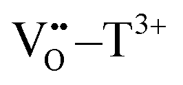 , and such a defect dipole is circled in a black dashed rectangle in Fig. 4(c2). In this case, Fig. 3(c) can be separated into three areas: the polarization differences in area-1 and area-3 are both attributed to Pi, while that in area-2 is caused by the combined effect of Pi and dipole polarization (Pd), which can be defined as a polarization double-enhancement. Such an effect enables higher Wrec to be triggered by a lower external electric field, giving the low-consumption character to the BCZT–0.15BZT ceramic. Another proof for such defect equations comes from the electron paramagnetic resonance (EPR) measurement, as seen in Fig. 4(d). The g factor in the spectra is calculated according to eqn (13),
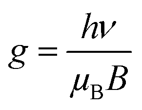
 .57,58 The peak for g ∼ 2.002 comes from
  , according to some latest works.59,60 As expected, a signal for Ti3+ is seen in the spectra of BCZT–0.15BZT, and the assumption above for eqn (5)–(9) can be thus confirmed.61 In general, for ceramics sintered at high temperatures, the reduction reaction of the Ti4+–Ti3+ transition occurs very often. But because the amount of Ti3+ coming from such a reaction is so tiny that the EPR test in our work cannot recognize it, the peak at g ∼ 1.980, symbolized for the Ti3+, only exists in BCZT–0.15BZT. The variations of defect equations with BZT doping content can also be confirmed by the Raman spectra, shown in Fig. 4(e). The spectrum of pure BCZT, which is measured as a control group in this work, is similar to that of a typical BaTiO3 ceramic, which is distinguished by the antiresonant dip at ∼174 cm−1, an A1 (TO) mode at ∼252 cm−1, and an E (TO) mode at ∼290 cm−1. For BCZT–xBZT with x being 0.10 to 0.17: (1) the wavenumber region below 200 cm−1 symbolizes the cation vibration of the A-site atoms, while the region from 200 to 450 cm−1 is caused by the bond vibration between B-site atoms O; (2) the wavenumber region from 450 to 650 cm−1 is correlated with the BO6 octahedra.62,63 The peak around 188 cm−1 becomes more and more diffused with increasing x. The peak around 290 cm−1, however, becomes diffused when x is increased from 0.10 to 0.12, and further x increments have no obvious effect on it. Peak diffusion is strongly related to the disorder of the lattice; such a phenomenon indicates that small doping of BZT affects both the A-site and the B-site, while extra doping only has more effect on the A-site. At this time, it is necessary for us to take a short look at the dielectric behavior of the BCZT–xBZT ceramics. Fig. S9 (ESI†) displays the temperature dependence of dielectric constant (ε–T curve) and dielectric loss (tan