
 Open Access Article
 This Open Access Article is licensed under a
 Creative Commons Attribution 3.0 Unported Licence
High Seebeck coefficient from isolated oligo-phenyl arrays on single layered graphene via stepwise assembly†
Xintai
Wang‡
*ab,
Ali
Ismael‡
 *cd,
Bashayr
Alanazi‡
ce,
Alaa
Al-Jobory
cf,
Junsheng
Wang
*b and
Colin J.
Lambert
*c
*cd,
Bashayr
Alanazi‡
ce,
Alaa
Al-Jobory
cf,
Junsheng
Wang
*b and
Colin J.
Lambert
*c
aZhejiang Mashang GM2D Technology Research Institute, Cangnan, Wenzhou, Zhejiang, China
bSchool of Information Science and Technology, Dalian Maritime University, Dalian, China. E-mail: wangjsh@dlmu.edu.cn; xintaiwang@dlmu.edu.cn
cPhysics Department, Lancaster University, Lancaster, LA1 4YB, UK. E-mail: c.lambert@lancaster.ac.uk; k.ismael@lancaster.ac.uk
dDepartment of Physics, College of Education for Pure Science, Tikrit University, Tikrit, Iraq
eDepartment of Physics, College of Science, Northern Border University, Arar, Kingdom of Saudi Arabia
fDepartment of Physics, College of Science, University of Anbar, Anbar, Iraq
First published on 9th October 2023
Abstract
Organic thin films composed of highly ordered molecular arrays hold tremendous potential for thermoelectric energy harvesting. In comparison to metal–thiolate arrays formed through covalent bonding, molecular arrays bound to graphene substrates via non-covalent interactions exhibit superior thermoelectric behavior. Recent studies have explored the thermoelectric properties of non-conjugated junctions utilizing graphene as a substrate. However, for energy-harvesting purposes, conjugated oligo-aromatic molecules with narrower HOMO–LUMO gaps are more desirable. The step-wise assembly strategy, which involves using a zinc-centered porphyrin to form a footpad first and subsequently binding the molecular backbones to the regularly arranged zinc centers in the footpad, has been reported as an effective approach for growing conjugated molecular backbone arrays, with minimal intermolecular effects on various types of substrates. In this study, we employ this strategy to fabricate aromatic molecular arrays on graphene substrates. Initially, a zinc-centered porphyrin layer is immobilized onto the graphene substrate through π–π stacking interactions. Subsequently, a conjugated pyridine backbone is coordinated to the zinc tetraphenylporphyrin (ZnTPP). Due to the substantial footprint of ZnTPP, this sequential assembly method effectively separates the molecular backbones and prevents smearing of the density of states arising from intermolecular interactions. Consequently, a significant enhancement in thermopower is achieved. Our findings present a novel approach for designing high-efficiency thermoelectric materials, resulting in a Seebeck coefficient of approximately 51 μV K−1. This value surpasses the majority of reported Seebeck coefficients for organic molecular junctions.
Introduction
Molecular-scale junctions, which utilize molecules as building blocks,1 offer the potential to revolutionize various technological applications, including transistors,2–4 sensors,5 memories,6 and thermoelectric energy harvesters.7–9 The electric and thermoelectric properties of molecular junctions have been extensively investigated in recent years, both at the level of individual molecules10–13 and self-assembled monolayers (SAMs).14–16 These studies have predominantly focused on noble-metal substrates like gold, silver, and platinum, together with organic molecular backbones, with specific anchor groups, such as thiolate,17–19 pyridine, fullerene,20,21 and large π systems.22,23 These anchor groups bind to a metallic substrate and facilitate the spontaneous formation of molecular layers on the substrate. Furthermore, the coupling strength between anchor group and substrate plays a crucial role in determining the quantum transport properties of the junction.7,16,24In thermoelectric energy harvesters, it is often desirable to have weak coupling between the anchor group and substrate. This weak coupling serves to effectively suppress interfacial phonon transport25 and prevent the broadening of molecular frontier orbitals, thereby significantly enhancing the thermoelectric conversion efficiency.26–28 Metallic substrates have the capability to form weak-coupling junctions with molecules through non-covalent interactions. However, these junctions are inherently unstable at room temperature, due to the high mobility of metal atoms.29,30 In order to address this issue, graphene has emerged as a promising alternative substrate for constructing non-covalent molecular junctions, utilizing anchor groups such as pyrene31,32 or amine33,34 to form self-assembled monolayers (SAMs). In comparison to their metal–thiolate counterparts, these graphene/molecule SAMs exhibit improved performance characteristics, including enhanced electric barrier behavior34 and superior thermoelectric properties.35
Most of the recently published graphene/molecule SAMs utilize alkyl chains as the molecular backbone. However, this type of backbone is not preferred in device applications due to its large HOMO–LUMO gap, which suppresses electron transport36,37 and thermopower.38 In order to overcome this limitation, molecules with conjugated systems, such as oligo-phenyl structures, are more attractive for molecular thermoelectric studies. Another issue that arises when scaling up single-molecule junctions to SAMs is the introduction of intermolecular interactions between the molecular backbones and their closely packed neighbors. These inter-backbone cross talks are known to have a strong influence on the measured quantum transport and thermoelectric behavior of SAMs.38,39 For instance, the broadening of the density of states resulting from intermolecular interactions leads to an increase in the width of the highest occupied molecular orbital (HOMO) and lowest unoccupied molecular orbital (LUMO) resonances, consequently reducing the efficiency of thermoelectric conversion;39 prolonged exposure to light radiation can induce cross-linking between the polyaromatic molecular backbone and its neighboring species, thereby disrupting the conjugation within self-assembled monolayers (SAMs);40 the intermolecular coupling opens additional tunneling path for electron transport, and this will quench the single molecule transport behaviour.41
Stepwise assembly represents an effective strategy for the formation of highly ordered molecular arrays on various types of substrates and has shown potential in addressing the aforementioned cross-talking issues. Morgado et al. utilized a zinc-entered porphyrin footpad and bipyridine wire to construct a supramolecular structure with a length of up to 14 nm on a highly oriented pyrolytic graphite (HOPG) substrate.42 Cea et al. described a layer-by-layer (LBL) approach to generate well-separated arrays of molecular backbones using zinc-centred porphyrin footpad and amine anchored molecular wire on gold substrate, which minimized the intermolecular interactions by the large intermolecular distance.43 In this study, we employed a similar approach to fabricate well-spaced arrays of oligo-phenyl wires on a single-layered (SL) graphene substrate. Firstly, zinc tetraphenyl porphyrin (ZnTPP, molecule 4 in Fig. 1(a)) was employed for the growth of a molecular thin film on SL chemical-vapor-deposited (CVD) graphene on a copper substrate. The immobilization of ZnTPP molecules on graphene was achieved through π–π stacking interactions (Fig. S47(b), ESI† denoted as Gr/4 in later text).44,45 Secondly, conjugated pyridine backbone molecules (molecules 5, 6, and 7 in Fig. 1(a)) were deposited onto the ZnTPP layer via zinc–pyridine coordinative bonds (Fig. 1(d), denotes as Gr/4/X where X denotes molecules 5–7) or (bilayers in later text). These backbones exhibited a perpendicular orientation with respect to the substrate due to their lone pair geometry and were isolated from each other by the large footprint of ZnTPP molecules (illustration in Fig. 1(b), AFM image in Fig. S47(c)–(e), ESI†).14,46 The thickness of both the ZnTPP layer and the bilayer self-assembled monolayers (SAMs) on graphene were estimated using the atomic force microscopy (AFM) technique, as illustrated in Fig. S48(a)–(d) (ESI†). The measured results obtained from AFM were found to be in good agreement with the corresponding thickness values estimated using density functional theory (DFT, Fig. S48(e), ESI†). This concordance between experimental and theoretical approaches further validates the bilayer growth. For comparative analysis, this work also investigated a series of alkyl amine molecules known to form high-quality self-assembled monolayers (SAMs) on graphene via non-covalent interactions (denote as Gr/X (X: 1–3)), as previously reported.33,34 These systems exhibit film thicknesses comparable to those of the stepwise assembled structures (Fig. 2), and the hydrophobic force between the alkyl backbones restricts the rotational degree of freedom of the SP3 carbon in the alkyl chain, thereby confirming the molecular configuration.47
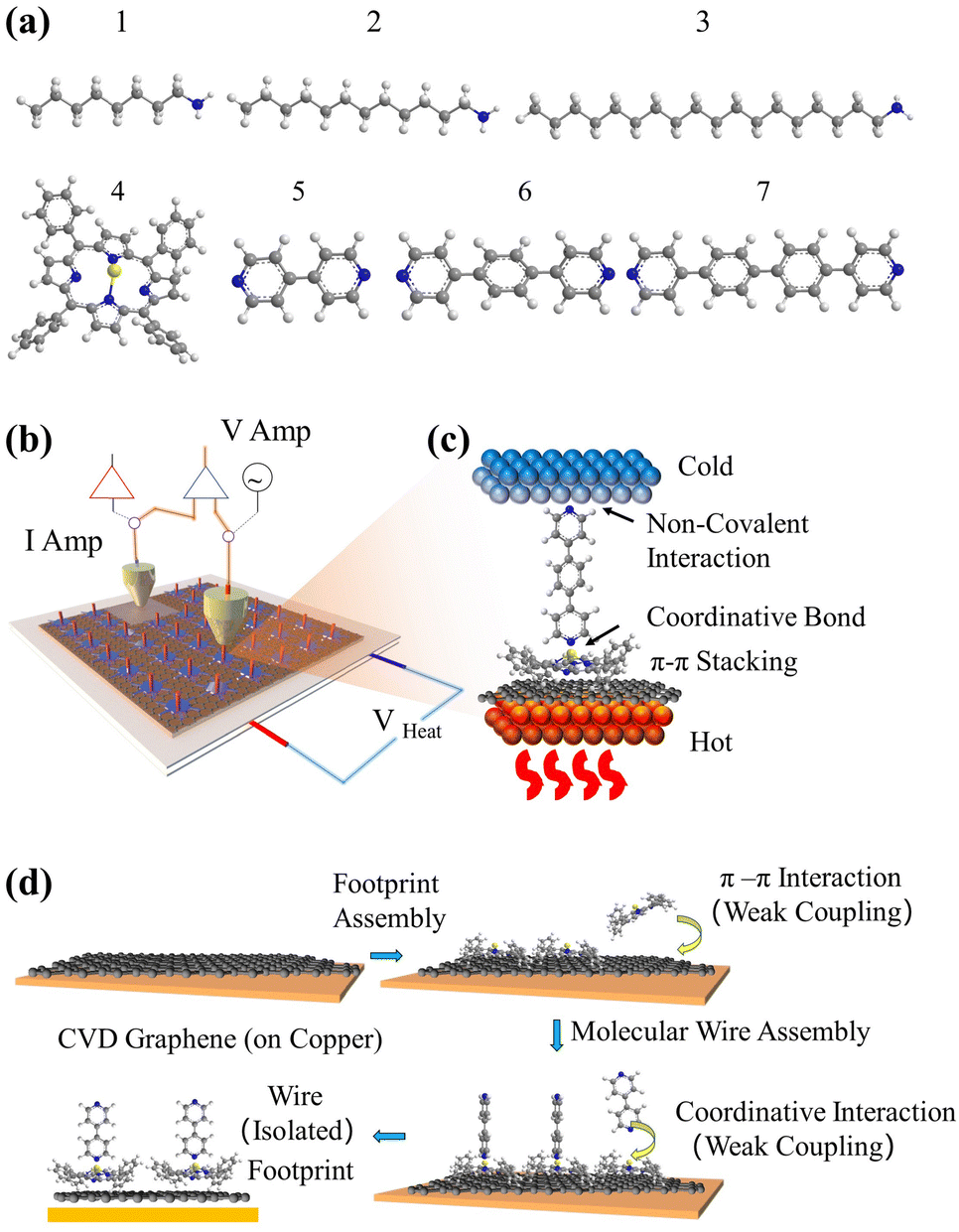 | ||
| Fig. 1 (a) 7 compounds used to construct SAMs, (b) scheme of measurement system used in this work, (c) an example of multi-component structure in EGaIn junction, and (d) the stepwise assembly strategy of forming molecular arrays. | ||
 | ||
| Fig. 2 8 junctions studied in this work. Monolayers including: Gr, Gr/1, Gr/2, Gr/3 and Gr/4. Bilayers including Gr/4/5, Gr/4/6 and Gr/4/7. | ||
Electron transport investigation
The electrical properties of self-assembled monolayers (SAMs) on graphene were investigated by constructing molecular junctions using eutectic Gallium Indium alloy (EGaIn) as the top electrode.48 EGaIn is a moldable non-Newtonian liquid metal. In this study, it was shaped into a cone-shaped tip, and the tip retained its shape due to the formation of a ∼0.7 nm native oxide outer shell (GaOx) upon contact with air.49,50 It has been proved that this type of tip can contact non-destructively with SAMs4,8–52 and form Cu/Gr/SAMs/GaOx/EGaIn junction.Fig. S51(a) (ESI†) depicts semi-log plots of current density versus bias voltage (J–V) curves for a series of Cu/graphene/NH2–CxHx+2/GaOx/EGaIn junctions (SAMs 1–3). The J–V characteristics for each type of SAM were collected from at least 80 J–V curves obtained on at least two independent samples prepared using the same method. Due to the large HOMO–LUMO gap of the alkyl backbones, electron transport in the junction occurs via coherent tunneling.53Fig. 3(a) illustrates the statistical distribution of conductances (G) at zero bias, derived from numerical differentiation for different alkyl linker junctions. The conductance value exponentially decreases with an increase in the number of CH2 units, as evidenced by the conductance–bias voltage (G–V) curves shown in Fig. S52(a) (ESI†).
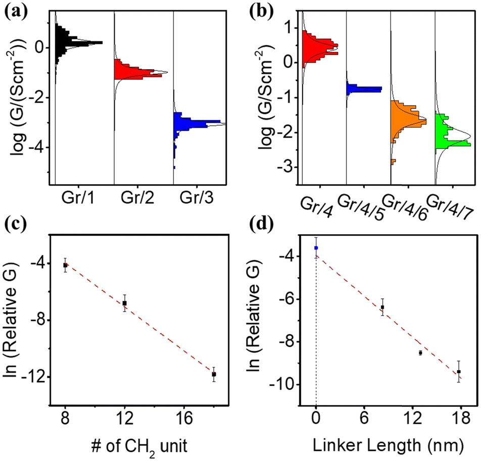 | ||
| Fig. 3 (a) G–V curve of Gr/SAMs/GaOx/EGaIn junction, SAMs molecule: 1, 2 and 3; (b) G–V curve of Gr/SAMs/GaOx/GaIn junction, SAMs molecule: 4, 4/5, 4/6 and 4/7. (c) Plot of ln(G) vs. number of alkyl unite for SAM 1–3. (d) Plot of ln(G) vs. linker length for SAM 4, 4/5, 4/6 and 4/7. Note relative conductance (relative G) is used in (c) and (d), the definition of relative G is explained in main text. | ||
One of the major challenges encountered when studying molecular transport using the EGaIn method is the significantly smaller effective electric contact area between the EGaIn tip and the SAMs layer compared to the physical contact area. Hence, accurately estimating the absolute conductivity of the SAM is difficult.54 In this study, a unitless relative conductivity was employed instead of absolute conductivity. The measured contact conductivity of Cu/graphene/Ga2O3/EGaIn was assigned a value of 1, and the conductivity of all the junctions was expressed relative to this value. The absolute conductivity values for all the junctions (in S cm−2) are listed in Table S1 (ESI†).
Fig. 3(c) shows a plot of ln(G) vs. the numbers of CH2 units. The linear relationship between ln(G) and molecular length confirms that transport is in the tunneling regime via expression:
| lnG) = ln(G0) − βd |
The fitted relative contact conductivity at d = 0 (G0) for alkyl-based SAMs on graphene was determined to be 9.0 ± 3.4. This value represents an order of magnitude increase compared to the measured contact conductivity (1). We attribute this difference to the complex contact interface between EGaIn and graphene, as the measurements were conducted under ambient conditions where contaminants, such as a thin film of water, can significantly reduce the measured current. In contrast, SAMs on graphene do not exhibit this issue due to their hydrophobic nature, which protects the surface from water contamination. As a result, SAM-modified graphene provides a more uniform contact and yields higher contact conductance.59
The electric behavior of the multi-component conjugated SAM-based junctions Gr/4/5, Gr/4/6 and Gr/4/7 were measured, with statistical results obtained from 80 J–V curves achieved on at least 2 independent samples (Fig. S51(b), ESI†). The corresponding numerical differential conductances at zero bias are shown in Fig. 3(b) (corresponding curves in Fig. S52(b), ESI†). The electric conductivity for the pyridine based oligo-phenyl linkers (molecule 5, 6 and 7) was expected to be higher than the alkyl linkers (molecule 1, 2, and 3) with similar lengths, because the delocalized electrons in the π system facilitate the electron transport process.60 However, the measured relative conductivity, G, for bipyridyl linker (Gr/4/5) was (1.7 ± 0.7) × 10−3, which was 10 times lower than the measured conductivity of an alkyl chain with similar tunneling lengths (Gr/1, (1.6 ± 0 0.4) × 10−2). This could be explained by three reasons: (1) the molecular packing density of the Gr/1 junction was determined by the surface area occupied by the alkyl chain. Conversely, the packing density of Gr/4/5 was determined based on the coverage area of molecule 4, which is established to be approximately 10–20 times larger than that of alkyl chains.23,61 Consequently, the number of parallel molecules per unit area formed with an EGaIn tip for Gr/4/5 was about 10–20 times lower than that of Gr/1. (2) For Gr/1, electrons tunnel through the amine–graphene interface directly, but for Gr/4/5 there were two interfacial tunnel barriers: the barrier between graphene and molecule 4, and the barrier between molecule 4 and molecule 5, which decreases the electron transmission probability. (3) In the Gr/4/5 junction, the molecular backbones (5) are isolated, thus the intermolecular transport path, which is known to increase electron transport efficiency,62 is absent.
The estimated tunneling decay factor for the pyridine based oligo-phenyl system was 0.33 ± 0.1 per nm (Fig. 3(d)), which is comparable with the formerly reported values on oligo-phenylene junction63 and other conjugated junctions,64,65 and significantly lower than that of alkyl based SAMs (Gr/1–3). This is expected, because of its smaller HOMO–LUMO gap. The fitted contact conductance for Gr/4/X (X = 5, 6, 7) junctions at d = 0, is calculated to be (G0 = 1.8 ± 0.4) × 10−2. This value agrees well with the measured Gr/4 junction without a pyridine linker, which is (2.6 ± 0.7) × 10−2.
Investigation of thermoelectric behavior
The thermoelectric properties of SAMs were investigated using a similar EGaIn setup, but with a Peltier stage and two thermocouples to control and measure the temperature difference (ΔT), and a differential voltage pre-amplifier to measure the thermovoltage created by ΔT (VTherm). The Seebeck coefficient of junction, S, was obtained via equation:7,8,35| VTherm = −S × ΔT |
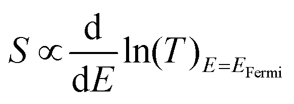
For each sample, VTherm from 5 different ΔTs were obtained, and linear curve fit was made between VTherm and ΔT for the 5 points. The negative of the slope of the curve was the Seebeck coefficient of the junction Fig. 4(a) shows the measured Seebeck distributions of alkyl junctions on graphene substrates, with different chain lengths. Each type of junction was measured on at least two independent samples prepared with the same recipe, and on each sample at least 3 independent spots were measured. For all the samples, good linearity between VTherm and ΔT was observed (Fig. S53–S59, ESI†). The slopes of linear fits for all junctions were negative, and therefore the Seebeck coefficients of the junctions were positive. This means that the electrode Fermi level was located closer to the HOMO resonance of molecular orbital.16,35 The Seebeck coefficients for 1–3 (C8, C12 and C18), junctions were 16.5 ± 8 μV K−1, 14 ± 9.5 μV K−1 and 13.5 ± 8 μV K−1 respectively, which are similar to the results reported by Yoon's group on the same system (8–15 μV K−1).35 It is important to mention that in Yoon's work,35 the Seebeck decreased with increasing alkyl chain lengths, whereas in the present work, the Seebeck coefficients for alkyl chains with different chain lengths were similar and within the standard deviation interval, no clear chain length-Seebeck dependency was observed. We believe it is due to the influence of the graphene on the Fermi level alignment relative to the molecular orbital energies. The Seebeck coefficient is depending on the change of transmission probability nearby Fermi region via the equation:
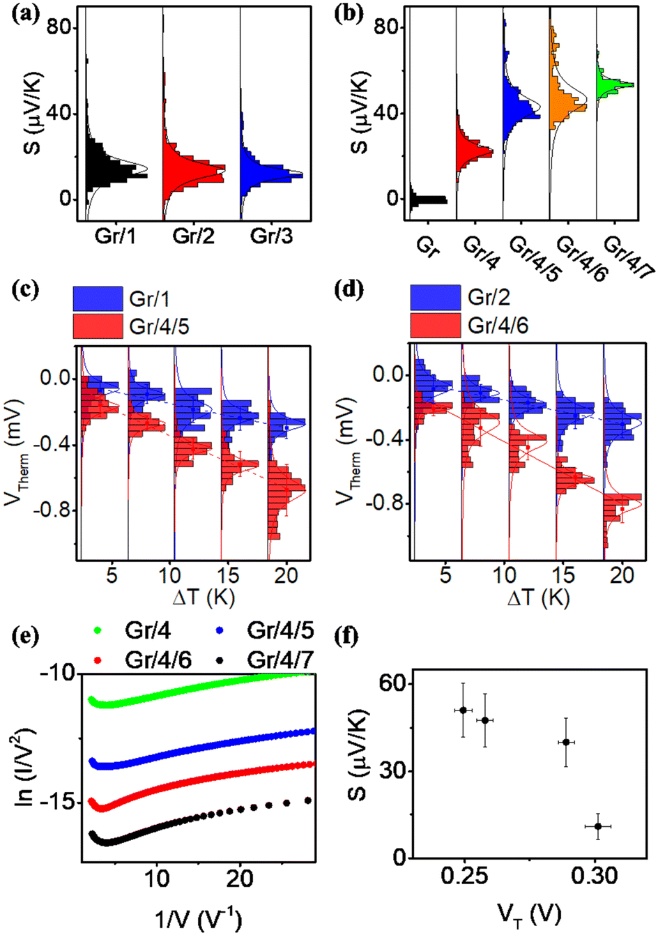 | ||
| Fig. 4 Thermoelectric properties of molecular junctions. (a) and (b) Statistics of Seebeck coefficient for all measured junctions. (c) and (d) Plots of VThermvs. ΔT for molecular junctions with comparable tunneling distance. (e) The Fowler Nordheim plot (FN) for Gr/4 and Gr/4/X (X: 5–7) junctions. (f) Measured Seebeck vs. transition voltage for Gr/4 and Gr/4/X (X: 5–7) junctions. | ||
For a derivation and discussion of the physical meaning of this equation, see Chapter 7 of the textbook.66
In our case, the electrode Fermi level is in the middle of the large HOMO–LUMO gap of the alkyl molecules, so the change of transmission slope is small and insensitive to the change the number of alkyl units.
Fig. 4(b) illustrates the measured Seebeck distribution of all conjugated molecular junctions on graphene substrates using a first layer of ZnTPP (molecule 4) as a footprint. The Seebeck coefficient for a ZnTPP layer adsorbed on graphene without the growth of a conjugated backbone (molecules 5–7) was determined to be 19 ± 4.4 μV K−1, which is approximately two times higher than that observed for ZnTPP on an Au substrate.23 Following the growth of second-layer pyridine-based conjugated backbones with varying lengths, the Seebeck coefficients increased to 40 ± 8.4 μV K−1 (Gr/4/5), 47.5 ± 9.1 μV K−1 (Gr/4/6), and 51 ± 9.2 μV K−1 (Gr/4/7). These values are about three times higher than those of alkyl linkers with comparable film thicknesses (Fig. 4(c) and (d)). This enhanced Seebeck behavior can be attributed to the fact that compared to alkyl chains, the conjugated oligo backbones have smaller HOMO–LUMO gaps, resulting in a steeper transmission slope near the electrode Fermi energy. It is worth mentioning that while pyridine-anchored molecules typically exhibit LUMO-dominated transport in metallic nanogaps, the pyridine backbone in this study displayed HOMO-dominated behaviour. This distinction arises from the presence of a series of interfaces in the Cu/Gr/4/X (X: 5–7)/GaOx/EGaIn junction, making the interfacial transport more intricate than direct metallic contact, and significantly influenced the energy-level alignment.
The measured Seebeck coefficients for Gr/4/X (X: 5, 6, 7) junctions were found to be higher than the Seebeck coefficients reported for most molecular (or SAM-based) junctions on gold substrates, which typically range from 5 μV K−1 to 30 μV K−1 in absolute value (as summarized in Table S3, ESI†). Specifically, when compared with thiol-anchored oligo-phenyl ring junctions on gold substrates at both the single molecule67 and SAM68 scales (S ∼ 8–13 μV K−1), where strong interfacial coupling occurs between the molecule and the substrate, the Seebeck coefficient achieved in this study was increased by about a factor of five. This enhancement can be attributed to the positioning of the Fermi level of the junctions in close proximity to the HOMO resonance, as indicated by our quantum calculations (Fig. S22, ESI†). In such a scenario, the presence of weak π–π interactions and the pyridine/Zn slippery interaction contribute to a reduction in the broadening of the HOMO and LUMO peaks. Consequently, this leads to a steepening of the transmission curve at the Fermi level, ultimately resulting in a high Seebeck coefficient. It is worth noting that the measured Seebeck coefficient in this work is significantly higher than our previously reported result for the Au/conjugated SAMs/ZnTPP/graphene/Pt junction (|S| ∼ 10–20 μV K−1).14 This difference arises, because in the present study, the molecular backbones are separated rather than closely packed, thereby suppressing the intermolecular couplings between the conjugated backbones. It has been demonstrated that different intermolecular coupling regimes can cause significant shifts in the transmission curves and influence the Seebeck coefficient of the junction.69 Additionally, it should be noted that the bottom electrode in this work is single-layer graphene, which possesses a different band structure compared to the previous study where multi-layered graphene was employed as the top electrode.70
Fig. 4(e) is the Fowler Nordheim plot (FN) for Gr/4 and Gr/4/X (X: 5–7) junctions. FN plots are a useful method for estimating the energy difference between the Fermi level and the nearest molecular frontier orbital. The minimum V for 1/V vs. I/V2 from the FN plot corresponds to the energy where transport changes from direct tunneling to FN tunneling, and is known as the transition voltage (VT). The transition voltage is not able to reveal if the Fermi level is closer to the HOMO or the LUMO, but can reveal the energy difference between the frontier orbital and the Fermi level. Fig. 4(f) showed the plot of measured Seebeck vs. transition voltage for Gr/4 and Gr/4/X (X: 5–7) junctions, and negative relationship was observed. This agreed with previous argument: as the number of oligo phenyl rings is increased, the Fermi-level moves closer to the HOMO resonance, which results in a decrease of the transition voltage and an increase of the Seebeck coefficient (the relationship between transition voltage and different junction was shown in Fig. S63, ESI†).
Fig. S61 (ESI†) shows the relationship between the measured current (in log scale, bias at 0.1 V) and thermovoltage of a Gr/4/5 molecular junction at ΔT = 4 K. The difference in current intensity is due to the different junction area between the probe and molecules (Fig. S40, ESI†). For junctions exhibiting low current, the thermovoltage is in the range of −120 to 200 μV (corresponding to 30–50 μV K−1). If a junction exhibits high current (log(I) > 0), the thermovoltage is significantly lower (about 10 μV). This value is similar to the Seebeck coefficient of Gr/EGaIn junctions, which indicates the presence of a short circuit between the tip and graphene, due to defects in the SAM layer for large-area junctions.68 The stability of the Gr/4/5 layer was tested by measuring the JV response for the freshly prepared sample and the sample leaving in air for 1 week. These were found to be almost identical, which indicates that the molecular layer is stable for at least a week (Fig. S60(a), ESI†). On the other hand, leaving the sample in air for 1 month caused the current density to increase significantly, indicating that the monolayer is no longer stable in the longer term, without encapsulation (Fig. S60(b), ESI†).
Theoretical simulations
To understand how the use of a graphene electrode affects the sign and magnitude of the Seebeck coefficient, we now compute the Seebeck coefficient of metal–molecule–metal and Gr–molecule–metal junctions. Although it is of interest to choose the metal to be EGaIn, in practice EGaIn (along with its unknown oxide layer) is too complicated to model reliably. Therefore, in what follows, we choose the metal to be gold. The use of gold, rather than EGaIn is in part supported by that fact that they have similar Fermi energies, because the work function of EGaIn was about 4.3 eV, which is close to the gold work function (4.8 eV).The transport properties of 16 junctions composed of monolayers and bilayers were modelled using a combination of density functional theory (DFT) and quantum transport theory. To calculate the electrical transport through monolayers 1–4, and bilayers 4/5, 4/6 and 4/7, we modelled junctions formed from the single molecules shown in Fig. S1 (ESI†) and the molecular bilayers shown in Fig. S2 (ESI†) (for more details see Section 1.1 in the ESI†).
As a first step towards understanding their electronic properties, their frontier orbitals and their energies were computed, as shown in Fig. S3–S9, ESI† (single molecules) and Fig. S10–S12, ESI† (molecular bilayers). Since we are studying multiple molecules with two different electrode materials, it is necessary to initially determine the optimal separation distance between these segments. Fig. S13–S19 (ESI†), show the binding energies between electrodes and molecules as a function of their separation. The optimum distances between the two components correspond to the energy minima of these curves and are summarized in Table S1 (ESI†), (for more details see Section 1.3 in the ESI†).
Fig. S20 and S21 (ESI†) show the 8 Au–Au and 8 Gr–Au junctions, of interest. Fig. S22–S27 (ESI†) show the transmission coefficients T(E) curves of the 8 Au–Au junctions. For single-molecule junctions (except ZnTTP), the simulations were non-spin-polarised, whereas for junctions containing ZnTTP, spin-polarised simulations were carried out. A similar approach is taken for Gr–Au junctions as shown in Fig. S28–S33, (for more details see Section 1.5 in the ESI†).
The right-most two columns of Table S2 in the ESI,† show the computed Seebeck coefficients of Gr–molecule–Au junctions are of opposite sign to those of Au–molecule–Au junctions. The results for the Gr-based junctions are reproduced in Table 2, which shows that the signs of the computed Seebeck coefficients of Gr–molecule–Au junctions are in agreement with the measured signs of experimental Gr–molecule–EGaIn junctions. (for more details see Sections 1.6 and 1.7 in the ESI†). Regarding the conductance comparison, Table 1, illustrates an excellent agreement between the theoretical Gr–molecule–Au junctions and the experimental Gr–molecule–EGaIn junctions.
| Junction | EGaIn experiment | Std | DFT |
|---|---|---|---|
| Relative G per area | (%) | (G/G0) | |
| Note: Conductance is relative to graphene conductance Gr. | |||
| Gr/1 | 1.6 × 10⁻² | 4 × 10⁻³ | 1.9 × 10⁻² |
| Gr/2 | 1.1 × 10⁻³ | 4 × 10⁻⁴ | 9.7 × 10⁻⁴ |
| Gr/3 | 7.4 × 10⁻⁶ | 2 × 10⁻⁶ | 6.5 × 10⁻⁶ |
| Gr | 1 | 6 × 10⁻² | 1 |
| Gr/4 | 2.6 × 10⁻² | 7 × 10⁻³ | 1.0 × 10⁻² |
| Gr/4/5 | 1.7 × 10⁻³ | 3 × 10⁻⁴ | 1.5 × 10⁻³ |
| Gr/4/6 | 2.0 × 10⁻⁴ | 8 × 10⁻⁵ | 1.4 × 10⁻⁴ |
| Gr/4/7 | 8.3 × 10⁻⁵ | 1 × 10⁻⁵ | 2.0 × 10⁻⁶ |
| Junction | EGaIn | Std | DFT |
|---|---|---|---|
| S (μV K−1) | S (μV K−1) | S (μV K−1) | |
| Gr/1 | 16.5 | 8 | 24 |
| Gr/2 | 14 | 9.5 | 16.5 |
| Gr/3 | 13.5 | 8 | 17 |
| Gr | −0.26 | 0.2 | −8 |
| Gr/4 | 11 | 4.4 | 14 |
| Gr/4/5 | 40 | 8.4 | 70 |
| Gr/4/6 | 47.5 | 9.1 | 178 |
| Gr/4/7 | 51 | 9.2 | 300 |
Conclusion
In this work, we demonstrate a stepwise method for fabricating multi-molecular-layer thermoelectric materials on a graphene substrate. Molecular backbones were separated with equal distances by using a ZnTPP footprint, which reduces intermolecular interactions. Results were compared with amine based non-conjugated junctions, with similar tunneling lengths. The electrical conductances of the molecular arrays exhibit a similar tunneling decay factor, as reported oligo-phenyl structures on a metal substrate. The Seebeck coefficient of the multi-component junction was about 3 times higher than the alkyl-based molecules, with comparable thickness, and higher than the Seebeck of most reported molecular junctions (>40 μV K−1). This demonstrates that step-wise assembly of well-spaced molecular layers on single layered graphene is an effective strategy for achieving large-scale high thermoelectric performance organic materials. Moreover, this work not only shows the potential of precise doping of molecular wires through intermolecular spacing, but also enables conjugated molecules to assemble on a single-layer graphene substrate, offering future possibilities to control the orbital alignment of SAMs through the utilization of a bottom gate.Author contributions
A. I., X. W., J. W. and C. L. conceived the concept. All authors approved the final version of the manuscript.Conflicts of interest
There are no conflicts to declare.Acknowledgements
This work was supported by the Leverhulme Trust for Early Career Fellowship ECF-2020-638 and the EPSRC Programe QMol EP/X026876/1. This work was additionally funded by the European Commission FET Open projects 767187-QuIET and 766853-EFINED. B. A. is grateful for financial assistance from Northern Border University (Saudi Arabia), and the Saudi Ministry of Education. A. K. I. and A. A. are grateful for financial assistance from Tikrit and Anbar Universities (Iraq), and the Iraqi Ministry of Higher Education (SL-20). X. W. acknowledge financial support from China National Youth Talent Program.References
- A. Aviram, Molecular Electronics – Science and Technology, Angew. Chem., Int. Ed. Engl., 1989, 28, 520–521, DOI:10.1002/anie.198905201.
- S. Das, et al., Molecularly Smooth Self-Assembled Monolayer for High-Mobility Organic Field-Effect Transistors, Nano Lett., 2016, 16, 6709–6715, DOI:10.1021/acs.nanolett.6b03860.
- H. Song, Electrostatic Gate Control in Molecular Transistors, Top. Curr. Chem., 2018, 376, 37, DOI:10.1007/s41061-018-0215-2.
- X. T. Wang, et al., Electrostatic Fermi level tuning in large-scale self-assembled monolayers of oligo(phenylene-ethynylene) derivatives, Nanoscale Horiz., 2022, 1201–1209, 10.1039/d2nh00241h.
- B. Kang, et al., Nanopatched Graphene with Molecular Self-Assembly Toward Graphene–Organic Hybrid Soft Electronics, Adv. Mater., 2018, 30, 1706480, DOI:10.1002/adma.201706480.
- C. E. Arcadia, et al., Multicomponent molecular memory, Nat. Commun., 2020, 11, 691, DOI:10.1038/s41467-020-14455-1.
- X. T. Wang, et al., Scale-Up of Room-Temperature Constructive Quantum Interference from Single Molecules to Self-Assembled Molecular-Electronic Films, J. Am. Chem. Soc., 2020, 142, 8555–8560, DOI:10.1021/jacs.9b13578.
- X. T. Wang, et al., Optimised power harvesting by controlling the pressure applied to molecular junctions, Chem. Sci., 2021, 12, 5230–5235, 10.1039/d1sc00672j.
- R. J. Miao, et al., Influence of Quantum Interference on the Thermoelectric Properties of Molecular Junctions, Nano Lett., 2018, 18, 5666–5672, DOI:10.1021/acs.nanolett.8b02207.
- R. J. Nichols and S. J. Higgins, Single Molecule Nanoelectrochemistry in Electrical Junctions, Acc. Chem. Res., 2016, 49, 2640–2648, DOI:10.1021/acs.accounts.6b00373.
- L. A. Wilkinson, et al., Assembly, structure and thermoelectric properties of 1, 1′-dialkynylferrocene ‘hinges’, Chem. Sci., 2022, 13, 8380–8387 RSC.
- J. Hurtado-Gallego, et al., Thermoelectric Enhancement in Single Organic Radical Molecules, Nano Lett., 2022, 22, 948–953, DOI:10.1021/acs.nanolett.1c03698.
- R. J. Davidson, et al., Conductance of ‘bare-bones’ tripodal molecular wires, RSC Adv., 2018, 8, 23585–23590 RSC.
- T. L. R. Bennett, et al., Multi-component self-assembled molecular-electronic films: towards new high-performance thermoelectric systems, Chem. Sci., 2022, 13, 5176–5185, 10.1039/d2sc00078d.
- G. D. Kong, M. Kim, S. J. Cho and H. J. Yoon, Gradients of Rectification: Tuning Molecular Electronic Devices by the Controlled Use of Different-Sized Diluents in Heterogeneous Self-Assembled Monolayers, Angew. Chem., Int. Ed., 2016, 55, 10307–10311, DOI:10.1002/anie.201604748.
- A. Ismael, et al., Molecular-scale thermoelectricity: as simple as ‘ABC’, Nanoscale Adv., 2020, 2, 5329–5334, 10.1039/d0na00772b.
- B. Han, et al., Systematic Modulation of Charge Transport in Molecular Devices through Facile Control of Molecule-Electrode Coupling Using a Double Self-Assembled Monolayer Nanowire Junction, J. Am. Chem. Soc., 2020, 142, 9708–9717, DOI:10.1021/jacs.0c02215.
- R. Ramachandran, et al., An Electromechanical Approach to Understanding Binding Configurations in Single-Molecule Devices, Nano Lett., 2018, 18, 6638–6644, DOI:10.1021/acs.nanolett.8b03415.
- A. Alshehab and A. K. Ismael, Impact of the terminal end-group on the electrical conductance in alkane linear chains, RSC Adv., 2023, 13, 5869–5873 RSC.
- X. K. Qiu, et al., Thiol-free self-assembled oligoethylene glycols enable robust air-stable molecular electronics, Nat. Mater., 2020, 19, 330–337, DOI:10.1038/s41563-019-0587-x.
- A. K. Ismael, 20-State Molecular Switch in a Li@ C60 Complex, ACS Omega, 2023, 8, 19767–19771 CrossRef CAS PubMed.
- S. V. Aradhya, M. Frei, M. S. Hybertsen and L. Venkataraman, van der Waals interactions at metal/organic interfaces at the single-molecule level, Nat. Mater., 2012, 11, 872–876, DOI:10.1038/Nmat3403.
- X. T. Wang, et al., Thermoelectric properties of organic thin films enhanced by pi-pi stacking, JPhys Energy, 2022, 4, 024002, DOI:10.1088/2515-7655/ac55a3.
- M. V. Solano, et al., Mono- and Bis(pyrrolo)tetrathiafulvalene Derivatives Tethered to C-60: Synthesis, Photophysical Studies, and Self-Assembled Monolayers, Chem. – Eur. J., 2014, 20, 9918–9929, DOI:10.1002/chem.201402623.
- Q. Li, M. Strange, I. Duchemin, D. Donadio and G. C. Solomon, A Strategy to Suppress Phonon Transport in Molecular Junctions Using pi-Stacked Systems, J. Phys. Chem. C, 2017, 121, 7175–7182, DOI:10.1021/acs.jpcc.7b02005.
- S. Zhao, et al., Non-covalent interaction-based molecular electronics with graphene electrodes, Nano Res., 2021, 16, 5436–5446, DOI:10.1007/s12274-021-3687-2.
- E. Cubukcu, K. Aydin, E. Ozbay, S. Foteinopoulou and C. M. Soukoulis, Subwavelength resolution in a two-dimensional photonic-crystal-based superlens, Phys. Rev. Lett., 2003, 91, 207401, DOI:10.1103/PhysRevLett.
- A. K. Ismael, et al., Exploring seebeck-coefficient fluctuations in endohedral-fullerene, single-molecule junctions, Nanoscale Horiz., 2022, 7, 616–625 RSC.
- E. Lortscher, Wiring molecules into circuits, Nat. Nanotechnol., 2013, 8, 381–384, DOI:10.1038/nnano.2013.105.
- F. Prins, et al., Room-temperature stability of Pt nanogaps formed by self-breaking, Appl. Phys. Lett., 2009, 94, 123108, DOI:10.1063/1.3109784.
- S. Seo, E. Hwang, Y. Cho, J. Lee and H. Lee, Functional Molecular Junctions Derived from Double Self-Assembled Monolayers, Angew. Chem., Int. Ed., 2017, 56, 12122–12126, DOI:10.1002/anie.201705518.
- P. Song, et al., Stable molecular diodes based on π–π interactions of the molecular frontier orbitals with graphene electrodes, Adv. Mater., 2018, 30, 1706322, DOI:10.1002/adma.201706322.
- B. Long, et al., Non-Covalent Functionalization of Graphene Using Self-Assembly of Alkane-Amines, Adv. Funct. Mater., 2012, 22, 717–725, DOI:10.1002/adfm.201101956.
- P. Song, et al., Noncovalent Self-Assembled Monolayers on Graphene as a Highly Stable Platform for Molecular Tunnel Junctions, Adv. Mater., 2016, 28, 631–639, DOI:10.1002/adma.201504207.
- S. Park, H. R. Kim, J. Kim, B. H. Hong and H. J. Yoon, Enhanced Thermopower of Saturated Molecules by Noncovalent Anchor-Induced Electron Doping of Single-Layer Graphene Electrode, Adv. Mater., 2021, 33, 2103177, DOI:10.1002/adma.202103177.
- J. Y. Son and H. Song, Investigation of intrinsic charge transport via alkyl thiol molecular electronic junctions with conductive probe atomic force microscopy, J. Mater. Sci.: Mater. Electron., 2022, 33, 13568–13573, DOI:10.1007/s10854-022-08291-w.
- D. J. Wold and C. D. Frisbie, Fabrication and characterization of metal-molecule-metal junctions by conducting probe atomic force microscopy, J. Am. Chem. Soc., 2001, 123, 5549–5556, DOI:10.1021/ja0101532.
- S. Park, N. Cho and H. J. Yoon, Two Different Length-Dependent Regimes in Thermoelectric Large-Area Junctions of n-Alkanethiolates, Chem. Mater., 2019, 31, 5973–5980, DOI:10.1021/acs.chemmater.9b02461.
- V. Obersteiner, D. A. Egger and E. Zojer, Impact of Anchoring Groups on Ballistic Transport: Single Molecule vs Monolayer Junctions, J. Phys. Chem. C, 2015, 119, 21198–21208, DOI:10.1021/acs.jpcc.5b06110.
- A. Beyer, et al., Fully cross-linked and chemically patterned self-assembled monolayers, Phys. Chem. Chem. Phys., 2008, 10, 7233–7238, 10.1039/b809787a.
- Y. R. Liu, et al., Intermolecular Effects on Tunneling through Acenes in Large-Area and Single-Molecule Junctions, J. Phys. Chem. C, 2020, 124, 22776–22783, DOI:10.1021/acs.jpcc.0c05781.
- Q. Ferreira, A. M. Braganca, L. Alcacer and J. Morgado, Conductance of Well-Defined Porphyrin Self-Assembled Molecular Wires up to 14 nm in Length, J. Phys. Chem. C, 2014, 118, 7229–7234, DOI:10.1021/jp501122n.
- E. Escorihuela, et al., Building large-scale unimolecular scaffolding for electronic devices, Mater. Today Chem., 2022, 26, 101067, DOI:10.1016/j.mtchem.2022.101067.
- G. Rotas, M. B. Thomas, R. Canton-Vitoria, F. D'Souza and N. Tagmatarchis, Preparation, Photophysical and Electrochemical Evaluation of an Azaborondipyrromethene/Zinc Porphyrin/Graphene Supramolecular Nanoensemble, Chem. – Eur. J., 2020, 26, 6652–6661, DOI:10.1002/chem.202000174.
- T. Phuangburee, et al., Surface modification of graphene oxide via noncovalent functionalization with porphyrins for selective photocatalytic oxidation of alcohols, New J. Chem., 2020, 44, 8264–8272, 10.1039/d0nj01141j.
- S. Winter, E. Weber, L. Eriksson and I. Csoregh, New coordination polymer networks based on copper(II) hexafluoroacetylacetonate and pyridine containing building blocks: synthesis and structural study, New J. Chem., 2006, 30, 1808–1819, 10.1039/b604591j.
- A. Ulman, Formation and structure of self-assembled monolayers, Chem. Rev., 1996, 96, 1533–1554, DOI:10.1021/cr9502357.
- R. C. Chiechi, E. A. Weiss, M. D. Dickey and G. M. Whitesides, Eutectic gallium-indium (EGaIn): A moldable liquid metal for electrical characterization of self-assembled monolayers, Angew. Chem., Int. Ed., 2008, 47, 142–144, DOI:10.1002/anie.200703642.
- C. S. S. Sangeeth, A. Wan and C. A. Nijhuis, Equivalent Circuits of a Self-Assembled Monolayer-Based Tunnel Junction Determined by Impedance Spectroscopy, J. Am. Chem. Soc., 2014, 136, 11134–11144, DOI:10.1021/ja505420c.
- M. Carlotti, et al., Two-Terminal Molecular Memory through Reversible Switching of Quantum Interference Features in Tunneling Junctions, Angew. Chem., Int. Ed., 2018, 57, 15681–15685, DOI:10.1002/anie.201807879.
- C. A. Nijhuis, W. F. Reus, J. R. Barber, M. D. Dickey and G. M. Whitesides, Charge Transport and Rectification in Arrays of SAM-Based Tunneling Junctions, Nano Lett., 2010, 10, 3611–3619, DOI:10.1021/nl101918m.
- N. Nerngchamnong, et al., The role of van der Waals forces in the performance of molecular diodes, Nat. Nanotechnol., 2013, 8, 113–118, DOI:10.1038/Nnano.2012.238.
- H. Song, Y. Kim, H. Jeong, M. A. Reed and T. Lee, Coherent Tunneling Transport in Molecular Junctions, J. Phys. Chem. C, 2010, 114, 20431–20435, DOI:10.1021/jp104760b.
- F. C. Simeone, et al., Defining the Value of Injection Current and Effective Electrical Contact Area for EGaln-Based Molecular Tunneling Junctions, J. Am. Chem. Soc., 2013, 135, 18131–18144, DOI:10.1021/ja408652h.
- V. B. Engelkes, J. M. Beebe and C. D. Frisbie, Analysis of the causes of variance in resistance measurements on metal-molecule-metal junctions formed by conducting-probe atomic force microscopy, J. Phys. Chem. B, 2005, 109, 16801–16810, DOI:10.1021/jp052348s.
- M. T. González, et al., Interference Controls Conductance in Phthalocyanine Molecular Junctions, J. Phys. Chem. C, 2021, 125, 15035–15043 CrossRef.
- B. Q. Xu and N. J. J. Tao, Measurement of single-molecule resistance by repeated formation of molecular junctions, Science, 2003, 301, 1221–1223, DOI:10.1126/science.1087481.
- X. P. Chen, H. T. Hu, J. Trasobares and C. A. Nijhuis, Rectification Ratio and Tunneling Decay Coefficient Depend on the Contact Geometry Revealed by in Situ Imaging of the Formation of EGaIn Junctions, ACS Appl. Mater. Interfaces, 2019, 11, 21018–21029, DOI:10.1021/acsami.9b02033.
- A. Kyrychenko, et al., Fluorescence Probing of Thiol-Functionalized Gold Nanoparticles: Is Alkylthiol Coating of a Nanoparticle as Hydrophobic as Expected?, J. Phys. Chem. C, 2012, 116, 21059–21068, DOI:10.1021/jp3060813.
- M. Wróbel, et al., Thermally Stable and Highly Conductive SAMs on Ag Substrate—The Impact of the Anchoring Group, Adv. Electron. Mater., 2021, 7, 2000947, DOI:10.1002/aelm.202000947.
- T. W. Schneider and D. A. Buttry, Electrochemical Quartz-Crystal Microbalance Studies of Adsorption and Desorption of Self-Assembled Monolayers of Alkyl Thiols on Gold, J. Am. Chem. Soc., 1993, 115, 12391–12397, DOI:10.1021/ja00079a021.
- H. Song, H. Lee and T. Lee, Intermolecular chain-to-chain tunneling in metal−alkanethiol−metal junctions, J. Am. Chem. Soc., 2007, 129, 3806–3807, DOI:10.1021/ja068875m.
- L. Venkataraman, J. E. Klare, C. Nuckolls, M. S. Hybertsen and M. L. Steigerwald, Dependence of single-molecule junction conductance on molecular conformation, Nature, 2006, 442, 904–907, DOI:10.1038/nature05037.
- B. Capozzi, et al., Length-dependent conductance of oligothiophenes, J. Am. Chem. Soc., 2014, 136, 10486–10492 CrossRef CAS PubMed.
- V. Kaliginedi, et al., Correlations between Molecular Structure and Single-Junction Conductance: A Case Study with Oligo(phenylene-ethynylene)-Type Wires, J. Am. Chem. Soc., 2012, 134, 5262–5275, DOI:10.1021/ja211555x.
- C. J. Lambert, Quantum transport in nanostructures and molecules, IOP Publishing, 2021 Search PubMed.
- P. Reddy, S. Y. Jang, R. A. Segalman and A. Majumdar, Thermoelectricity in molecular junctions, Science, 2007, 315, 1568–1571, DOI:10.1126/science.1137149.
- S. Park and H. J. Yoon, New Approach for Large-Area Thermoelectric Junctions with a Liquid Eutectic Gallium-Indium Electrode, Nano Lett., 2018, 18, 7715–7718, DOI:10.1021/acs.nanolett.8b03404.
- X. X. Fu, L. X. Zhang, Z. L. Li and C. K. Wang, Switching properties of bi-OPE-monothiol molecular junctions: Substituent effects and improvement of open-close ratio, Chin. Phys. B, 2013, 22, 028504, DOI:10.1088/1674-1056/22/2/028504.
- C. R. C. Rêgo, L. N. Oliveira, P. Tereshchuk and J. L. Da Silva, Comparative study of van der Waals corrections to the bulk properties of graphite, J. Phys.: Condens. Matter, 2015, 27, 415502, DOI:10.1088/0953-8984/27/41/415502.
Footnotes |
| † Electronic supplementary information (ESI) available. See DOI: https://doi.org/10.1039/d3tc02842a |
| ‡ These authors contributed equally to this work. |
| This journal is © The Royal Society of Chemistry 2023 |