DOI:
10.1039/D3TC02651E
(Paper)
J. Mater. Chem. C, 2023,
11, 14680-14694
A conceptual framework for designing and analyzing complex molecular circuits†
Received
26th July 2023
, Accepted 7th October 2023
First published on 9th October 2023
Abstract
Assembling and prototyping circuits on a common breadboard scaffold is critical for developing functional single molecule electronic devices. To this end, we recently demonstrated a bis-terpyridine-based molecular breadboard (TPm) junction with conductance readouts which were linear superpositions of five single terminal embedded circuits. Here, we present a full computational framework to create molecular breadboards with the ability to replace/alter individual circuit components. By applying the framework to the bis-terpyridine-based breadboard, we show that the relative conductance of the five constituent single terminal circuits can be varied by more than an order of magnitude by repositioning electrode anchoring nitrogen atoms. Specifically, by placing nitrogen atoms at meta (TPm), ortho (TPo), and para (TPp) positions on the pyridyl rings, individual circuits are tuned by altering destructive multi-orbital quantum interference effects (QIE) and the relative electrode accessibility (REA) of anchoring nitrogen atoms. We introduce a phase-plot analysis to highlight the interdependence of QIE- and REA-induced changes in the conductance of each single terminal circuit in the breadboard. Our studies predict a QIE-induced boost in circuit conductance for TPp relative to TPm which is insensitive to REA. In contrast, REA suppresses the QIE boost for circuit conductance in TPo relative to that in TPm. Our computational framework for designing breadboard junctions includes new quantitative tools to estimate thermal weights of molecular conformations, the relative electrode accessibility of anchoring atoms, and the extent of constructive/destructive quantum interference in charge transport mediated by multiple orbitals. These advances should be also useful for the analysis of other molecular junctions.
1. Introduction
The field of molecular electronics aims to develop functional devices with capabilities distinct from semiconductor-based electronics.1–3 Thus far, break junction techniques4–6 and computational methods7 have demonstrated that molecules can function as wires,8,9 switches,10–12 rectifiers,13,14 transistors,15 and potentiometers.16 To create functional devices, it is essential to assemble molecular electronic components on a single scaffold akin to a printed circuit board in conventional electronics. This need was recognized very early in the field17,18 and it was proposed that complex functional circuits could be created by linking individual molecular electronic components. However, a direct naive implementation of the proposal is problematic18 because strong electronic couplings and the quantum nature of charge transport would destroy the functionalities of the individual circuit elements connected by covalent chemistry or self-assembly. Furthermore, in some cases, functionality of an electronic component originates from the electrode–molecule interface14,19 which might be destroyed by linking components together. A key step towards developing complex molecular circuits was the proposal of quantum superposition rules by Joachim and co-workers to provide the total conductance of two molecular units in series or in parallel,20,21 which were verified in single molecule junction experiments.22,23 More recently, in a joint theoretical and experimental study,24 we demonstrated that up to five single terminal circuits could be combined within a bis-terpyridine-based molecular junction (TPm) with six electrode-anchoring pyridyl linkers. The study on TPm showed that the break-junction setup facilitates the prototyping of distinct superpositions of circuits within molecules with multiple (more than two) anchoring groups akin to a breadboard used in the conventional macroscopic electronics. The concept of breadboard, as introduced by us, is applicable to molecules which possess more than two anchoring groups thereby enabling access to multiple pre-enclosed/embedded current flow pathways within a single scaffold.24–28 Here, we present a computational framework which enables us to tune/modify electronic properties of individual circuit elements embedded within the molecular breadboard by using simple chemical design principles.
In the manuscript, we will demonstrate that by changing the positions of the anchoring groups (Fig. 1A and B), it is possible to change the relative conductance of the five single-terminal “basis” circuits (Fig. 1C) within a bis-terpyridine-based molecular scaffold. Note that the basis circuits in Fig. 1C are not different molecules, rather they are embedded circuits within the bis-terpyridine breadboards (Fig. 1B). By placing the electrodes in five different positions across the molecules in Fig. 1B so that they contact the terminal N-atoms separated by two, three, four, and five rings, we obtain the 2r, 3rm, 3rp, 4r, and 5r basis circuits of Fig. 1C respectively. Our previous study showed that each of four conductance states of TPm resolved in break-junction experiments can be expressed as a linear superposition of the conductance of these five single terminal circuits.24 In terms of the rules presented by Joachim and co-workers,20 for each of these five basis circuits, nodes are not present inside the tunneling junction, but rather are placed at the ends. Therefore, in the weak bias limit, these circuits show Ohmic currents and can be considered to be resistors. Furthermore, as shown analytically in our previous study,24 within the weak coupling limit such that molecule–electrode coupling is much smaller than the tunnelling barrier, the conductance of multi-terminal contact configurations is given by a superposition of the conductance of basis circuits. Moving forward, in the present manuscript we propose that simple modifications to the breadboard design which are accessible to synthetic chemistry can alter the transport properties of constituent basis circuits. Such design elements include site-selective chemical substitutions/functionalization, modifications in the ring connectivity, choice of anchoring groups and anchoring group placement, all of which have been successfully used to modulate charge transport in single molecule junctions.19,29 Here, we showcase how the last possibility enables us to the change the conductance of each of the five basis circuits shown in Fig. 1C. Furthermore, molecular breadboards differ from conventional breadboards in terms of their conformational flexibility, the microscopic nature of the electrode–molecule contact, and the presence of quantum mechanical effects. Our computational approach addresses each of these challenging aspects by providing quantitative tools (vide Infra) which are also demonstrated to be transferrable to the analysis of electronic transport in any single molecule junction.
 |
| | Fig. 1 (A) A bis-terpyridine-based molecular breadboard with multiple anchoring atoms accessible to nano-electrodes in a break-junction setup. Here, we propose that changing the position of anchoring nitrogen atoms (red, green blue) serves to change the conductance of circuit elements in the molecular breadboard. Conceptually, the modulation of conductance can be accomplished by altering QIE between the limits of fully destructive/constructive quantum interference (DQI/CQI) and/or REA between the limits of low to high electrode accessibility. (B) Skeletal structure of TPm, TPo, and TPp with peripheral pyridyl N-atoms placed at meta, ortho, and para positions, respectively. (C) 2–5 ring single terminal basis circuits of the TPm/o/p molecular breadboard obtained by placing electrodes in five different configurations attached to nitrogen atoms either on the same terpyridine arm (2r and 3rm) or across both arms (3rp, 4r, and 5r) for the molecules in panel B. In ref. 24, we showed that each of the four experimentally resolved TPm conductance states originated from a linear combination of these basis circuits. Red, blue, and green dots in C represent nitrogen substitution positions for each basis circuit in the TPo, TPm, and TPp breadboards respectively. | |
The single-molecule electronic conductance depends on molecular structure,30,31 electrode-interfacing linker groups,8,28,32–34 and molecular binding geometries.25,27,35 Additionally, external factors such as solvation36 and electrochemical gate bias37 are also important. An exciting prospect is to utilize these factors to harness quantum interference phenomena within the molecular junctions.38–42 Such quantum interference effects (QIE) have been utilized previously to manipulate the room temperature coherent electronic conductance in a variety of molecular junctions.33,43 Here, we propose to manipulate QIE in the five basis circuits by changing the placement of the peripheral ring N-atoms from meta to ortho/para positions (Fig. 1). To this end, we developed an analysis to quantify the multi-orbital QIE in the breadboard molecules. Re-positioning of the peripheral N-atoms in the breadboard scaffold also impacts both, their electrode accessibility and molecular conformation. We therefore developed a microscopic model of electrode–molecule interactions to estimate the relative electrode accessibility (REA) of anchoring groups independent of their placement on a conformationally flexible molecular scaffold. The new model also rigorously validates the REA for core N-atoms in TPm estimated in our previous study.24 Furthermore, we present an algorithm that uses molecular symmetry to systematically enumerate the breadboard conformations and estimate their thermal contributions to the conductance. Finally, since REA and QIE are simultaneously affected by repositioning of the N-atoms in the scaffold, we introduce a phase plot analysis to study their interdependence. We apply each quantitative tool developed here (multi-orbital QIE analysis, conformational sampling algorithm, and REA estimator) to simple examples to highlight their utility for studying any molecular junction in general.
2. Results
2.1. Conductance distributions for the TPx (x = m/o/p) breadboards
We used the computational framework described in Methods Subsections 5.1–5.5 to generate thermally weighted conductance distributions of TPx breadboards assuming full electrode accessibility for peripheral and core N-atoms (i.e., no REA effects).
Thermal populations of the DFT-optimized geometrically distinct TPx breadboard conformations (see Methods subsection 5.2 and ESI,† Sections S1–S3) are binned in in Fig. 2A–C based on their energy values. The conformational energy range for the three molecules varies significantly (∼4.7kBT, ∼45.5kBT, and ∼0.7kBT for TPm/o/p, respectively, where temperature T = 300 K and kB is the Boltzmann constant) creating a diversity in thermally accessible conformations across the breadboards. The thermal Boltzmann weight for conformation i of breadboard B is
| |  | (1) |
where, Δ
GF(
i) is the free energy of the conformation. The thermal weights for the conformations are plotted (brown dots) in
Fig. 2A–C as a function of energy. For TP
p, all 20 conformations are thermally accessible with weights ranging from 4–7%. In contrast, for TP
o, only two conformations appear thermally accessible with the weights ∼80% and ∼20%. The TP
m breadboard presents an intermediate case with weights in the range ∼0.04–5%. Adopting a uniform protocol, we computed the conductance distributions for all five basis circuits (
Fig. 1C) in TP
x breadboards, utilizing all molecular conformations with their thermal weights (
eqn (1) and (14)).
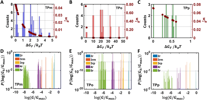 |
| | Fig. 2 Free energy histograms for the conformations of (A) TPm (bin width = 0.1), (B) TPo (bin width = 1), and (C) TPp (bin width = 0.02). In each panel, Boltzmann weights (right y-axis) of the conformations (eqn (1)) are plotted as a function of energy (brown dots). Probability weights (eqn (2)) of the basis circuit conductance for (D) TPm, (E) TPo, and (F) TPp breadboards (bin width = 0.01). The conductance values are normalized relative to the highest conductance value Gmax (that of a 2r TPo circuit). | |
In Fig. 2D–2F, we plot the distributions of log-normalized conductance log(G/Gmax) for the five basis circuits from geometrically distinct TPx breadboard conformations. The conductance is normalized with respect to the highest conductance Gmax (that of a 2r TPo circuit) in the dataset. The overall probability weight (Y-axis in Fig. 2D–F) for an n-ring (nr) basis circuit of breadboard B in a bin centered at log(Gk/Gmax) is given by:
| |  | (2) |
with
. Here, index
i runs over all the distinct geometries of B;
x is the number of n-ring circuits in the breadboard conformation
i with conductance values lying in the bin centered at log(
Gk/
Gmax);
Nnr is the multiplicity of an n-ring circuit (4 × 2r, 2 × 3rm, 1 × 3rp, 4 × 4r, and 4 × 5r) in the TP
x scaffold. The multiple conductance peaks for each circuit in the three breadboards (
Fig. 2D–F) arise from heterogeneities in the thermally accessible molecular conformations (see ESI,
† Section S4 for details). Further, within each breadboard, the conductance distributions for the basis circuits are roughly ordered by the end-to-end circuit length (2r > 3rm > 3rp > 4r > 5r) with a single exception (
G3rp >
G3rm). Further, comparing the breadboards, the basis circuit conductance (excluding the invariant 3rp circuit) in TP
m is lower than that for circuits in TP
o (
Fig. 2D and E) and in TP
p (
Fig. 2D and F). The lower conductance of the 3rm circuit relative to 3rp and the relative conductance trends for corresponding basis circuits across the three breadboards is in accordance with the quantum circuit rules demonstrated by Manrique
et al. for OPE-based molecules.
33 Essentially, a
meta-placement of the peripheral pyridyl N-atoms and
meta ring connectivity both lower conductance relative to the corresponding molecules with
para/
ortho N-atom placement and
para-ring connectivity. While the differences in the breadboard conformations could also potentially contribute, we show in the following subsections that these conductance trends are primarily due to QIE.
2.2. Tuning the relative conductance of basis circuits with pure QIE in the presence of REA
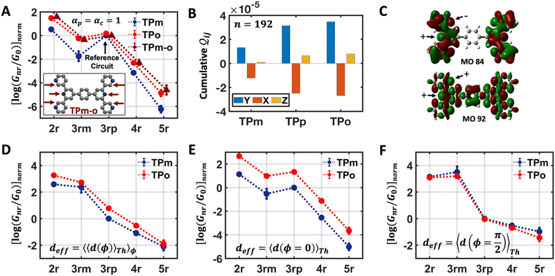
In this subsection, we demonstrate a QIE induced boost in basis circuit conductance upon changing the peripheral pyridyl ring N-atoms from meta (TPm) to para (TPp) position in the presence of REA. To separate out conformational contributions, we consider a fictitious breadboard24 wherein the electrodes exclusively contact the para-atoms of TPm (depicted as TPm-p in Fig. 3A). Since the conformations of TPm-p are the same as TPm, relative changes in basis circuit conductance across the two breadboards can be assigned purely to QIE. In Fig. 3A, we first present the conductance of all five basis circuits for TPm, TPp, and TPm-p calculated excluding REA effects. The decay in conductance is non-monotonic with respect to the circuit/tunneling lengths which are comparable in the breadboards (Fig. 3A and ESI,† Fig. S9A). For instance, the tunneling conductance of the 3rp circuit is comparable to the shorter 2r and ∼56-fold higher than that of shorter 3rm circuit (blue data in Fig. 3A). The suboptimal conductance values for the shorter 2r and 3rm circuits are presumably due to the meta placement of the anchoring N-atoms (2r and 3rm) and meta-connectivity of the pyridyl rings (3rm). We expect the QIE in TPp to be altered relative to that in TPm due to the altered positions (para versus meta) of the peripheral N-atoms. Indeed, the conductance of 2r is more than an order of magnitude higher than that of 3rp in TPp (green vs. blue data Fig. 3A). Further, the difference in conductance between 3rm and 3rp reduces in TPp relative to that in TPm (green vs. blue data in Fig. 3A). Note that 3rp serves as a reference circuit as it remains unchanged (Fig. S4D and F, ESI†) and has nearly identical conductance in TPm and TPp. By comparing the conductance of the 3rp circuit and the 3rm circuits in the two breadboards (data in Fig. 3A), it is possible to estimate the conductance drop purely due to the meta connectivity of rings (〈log(GTPp3rp/G0)〉 − 〈log(GTPp3rm/G0)〉 ≈ 0.85) and that owing purely to the meta-placement of the pyridyl N-atoms (〈log(GTPp3rm/G0)〉 − 〈log(GTPm3rm/G0)〉 ≈ 0.86). We find that the conductance of all basis circuits (except 3rp) in TPp are higher than that of their counterparts in TPm. This boost in conductance for each basis circuit in TPp is almost the same as that obtained for the TPm-p breadboard (green solid circles versus brown solid triangles in Fig. 3A) relative to TPm. This clearly shows that the differences in the conformations of TPm and TPp are not large enough to influence the conductance, and the changes in the basis circuit conductance between the breadboards is purely due to QIE (vide infra). Comparing TPm and TPp, the 4r circuit shows the lowest QIE boost (∼4-fold), while 5r circuit shows the highest QIE boost (∼11-fold).
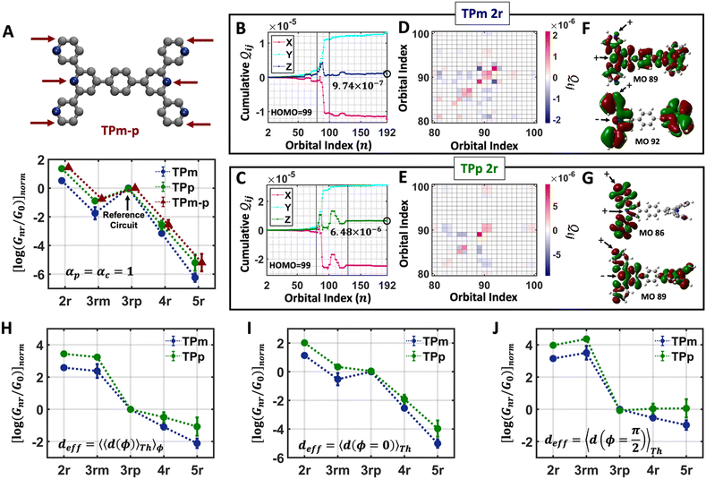 |
| | Fig. 3 (A) Basis circuit conductance in TPm, TPp, and TPm-p in the absence of REA (all N/C atoms have equal electrode accessibilities). In the TPm-p breadboard (top), to form 2r, 3rm, 3rp, 4r, and 5r basis circuits, the two electrodes contact any two atoms from the set marked with arrows (four peripheral ring para carbons and two core ring nitrogens of TPm molecule). The plot shows thermal average values and standard deviations (eqn (13) and (14)) over conformations. The subscript “norm” in the y-label implies that all the log(G/G0) values are uniformly shifted with respect to the average 〈log(GTPm3rp/G0)〉 for reference 3rp circuit in TPm. The data for TPm-p is offset along X-axis for better visualization. (B) and (C) Cumulative (sum over orbitals)  -matrix elements: Pure contributions from MOs -matrix elements: Pure contributions from MOs  (cyan), QI contributions (cyan), QI contributions 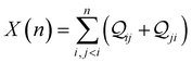 (magenta), and the overall cumulative transmission Z(n) = X(n) + Y(n) (blue/green for TPm/p respectively) for 2r circuit in the most thermally accessible conformation of TPm and TPp. Data for other circuits is shown in ESI,† Fig. S11. (D) and (E) Heatmap showing (magenta), and the overall cumulative transmission Z(n) = X(n) + Y(n) (blue/green for TPm/p respectively) for 2r circuit in the most thermally accessible conformation of TPm and TPp. Data for other circuits is shown in ESI,† Fig. S11. (D) and (E) Heatmap showing  -matrix elements for dominant MOs (80–100) representing pure orbital contributions and interference contributions between pair of MOs for TPm and TPp. Heatmap for all orbitals are provided in ESI,† Fig. S12 and S13 (F)–(G) Orbitals that show highest DQI for the 2r circuit in the most thermally accessible conformation of TPm and TPp. The arrows show orbital phases (+/−) on terminal N-atoms (H)–(J) Basis circuit conductance (thermal averages and standard deviations) with REA (eqn (13)–(15)) for TPm and TPp based on three different models for estimating the effective screening length deff for the anchoring N-atoms as indicated in the panels (see also Methods Subsection 5.4). -matrix elements for dominant MOs (80–100) representing pure orbital contributions and interference contributions between pair of MOs for TPm and TPp. Heatmap for all orbitals are provided in ESI,† Fig. S12 and S13 (F)–(G) Orbitals that show highest DQI for the 2r circuit in the most thermally accessible conformation of TPm and TPp. The arrows show orbital phases (+/−) on terminal N-atoms (H)–(J) Basis circuit conductance (thermal averages and standard deviations) with REA (eqn (13)–(15)) for TPm and TPp based on three different models for estimating the effective screening length deff for the anchoring N-atoms as indicated in the panels (see also Methods Subsection 5.4). | |
Here, using  -factor analysis (Methods Subsection 5.3 and ESI,† Section 6) we show that all the basis circuits in the TPm and TPp breadboards exhibit destructive multi-orbital quantum interference (DQI) and attribute the variations in conductance within and across the breadboards to the differing extents of DQI. In Fig. 3B and C, we present data for the most thermally accessible (highest wBi) conformations of 2r in TPm and TPp breadboards (ESI,† Fig. S11 shows data for other basis circuits). Fig. 3B shows cumulative diagonal (pure contributions Y) and off-diagonal (quantum interference contributions X) elements of the
  -matrix along with their sum (the transmission Z) for TPm as a function of orbital index (n). The corresponding data for TPp is presented in Fig. 3C. While the total transmission from all MOs (Z(n = 192)) for the 2r circuit in TPp is higher than that in TPm, it is apparent that 2r circuits in both breadboards show DQI (X(n = 192) < 0 in Fig. 3B and C). In fact, all five basis circuits in TPm and TPp exhibit DQI (ESI,† Fig. S11). However, the DQI is lower for all circuits in TPp relative to those in TPm leading to the observed differences in conductance values (Fig. 3A). Further, the quantum interference is clearly multi-orbital in nature. For instance, strong conductance contributions arise from MOs 80–100 and MOs 80–130 for 2r in TPm and TPp respectively (data between the two black vertical lines in Fig. 3B and C). A decomposition of the pure
  and quantum interference contributions
  for dominant MOs 80–100 of the 2r circuit shows (Fig. 3D and E) that while contributions from MO pairs interfere both destructively and constructively, the total interference from dominant MOs is DQI. In Fig. 3F and G, we visualize MO pairs with the highest DQI for the 2r circuit in TPm and TPp respectively. The DQI originates from the differences in signs of orbital amplitudes at the terminal N-atoms (arrows in Fig. 3F and G).
Next, we examine conductance trends with REA (Fig. 3H) using the thermally averaged effective screening length (eqn (10) and (15)). In this case, αp = 1 for both TPm and TPp and the electronic coupling for the core N-atoms in both breadboards is two orders of magnitude smaller than that for the peripheral N-atoms (see Table 2). Note that the attenuation ratio value (αp/αc = 115.8) for TPm agrees well with the value—116—that described MCBJ experiment data.24 Thus, the relative conductance trends for the basis circuits (which contain different combinations of peripheral and core N-atom termini) within each of the two breadboards are altered significantly upon including REA (compare trends in Fig. 3H and A). However, the REA for the core and peripheral N-atoms (αp and αc) in TPm and TPp are both comparable. Therefore, the boost in conductance for the basis circuits in TPp relative to that in TPm due to QIE is not altered upon including REA (compare differences in blue and green data values in Fig. 3H and A). We find that more restricted estimates of REA based on deff = 〈d(ϕ = 0)〉Th and  produce lower and upper bounds for αc leaving αp unchanged (Table 2). The conductance of basis circuits for REA with deff = 〈d(ϕ = 0)〉Th are close to pure QIE trends (compare Fig. 3I and A). On the other hand, REA with
  alters the relative conductance trends across the five basis circuits within each breadboard (compare Fig. 3H and J). Nevertheless, the relative boosts in the basis circuit conductance between TPp and TPm produced by QIE are still preserved with the new REA estimates since both αp and αc for the two breadboards remain comparable.
2.3. Changes in REA can suppress QIE induced relative circuit conductance trends across breadboards
In this subsection, we demonstrate the combined action of QIE and REA in altering the relative basis circuit conductance in TPx breadboards by moving the peripheral ring N-atoms from meta (TPm) to ortho (TPo) position. To separate out conductance changes due to conformations and those purely due to QIE, we consider a fictitious TPm-o breadboard (inset in Fig. 4A) wherein the electrodes exclusively contact the ortho atoms of TPm. We first discuss the basis circuit conductance trends in the absence of REA. The conductance is observed to drop non-monotonically with circuit/tunneling length for both TPm and TPo (Fig. 4A). The 3rp circuits in the two breadboards, which have identical end-to-end lengths, (ESI,† Fig. S9B) and very similar conformations (ESI,† Fig. S4D and E) serve as a reference circuit to compare conductance trends. Whereas, the conductance values of the 3rp reference circuit were virtually indistinguishable in TPm and TPp (Fig. 3A), they are slightly different for TPm and TPo (Fig. 4A) due to variations in the conformations of these breadboards (ESI,† Fig. S4D–F). Interestingly, the conductance of 3rp, 4r, and 5r circuits in TPo are significantly different despite these circuits having similar lengths. This trend can be attributed to QIE arising from differences in ring connectivities of the circuits. All basis circuits (except the 3rp reference circuit) in TPo show higher conductance relative to their counterparts in TPm. A comparison of the basis circuit conductance values in TPo and TPm-o (red solid circles versus brown solid triangles in Fig. 4A) relative to TPm reveals that the boost in the conductance is primarily due to the changes in QIE (vide infra) arising from moving the peripheral N-atoms from meta to ortho positions. The boost in the basis circuit conductance for TPo relative to TPm is slightly larger than that for TPp because of the shorter lengths of the TPo basis circuits relative to their TPp counterparts.
 |
| | Fig. 4 (A) Basis circuit conductance in TPm, TPp, and TPm-o in the absence of REA (all N/C atoms have equal electrode accessibilities). In the reference TPm-o breadboard (inset), to form 2r, 3rm, 3rp, 4r, and 5r basis circuits, the two electrodes contact any two atoms from the set marked with arrows (four peripheral ring ortho carbons and two core ring nitrogens of a TPm molecule). The plot shows thermal average values and standard deviations (eqn (13) and (14)) over conformations. The subscript “norm” in the y-label implies that all the log(G/G0) values are uniformly shifted with respect to the average 〈log(GTPm3rp/G0)〉 for reference 3rp circuit in TPm. The data for TPm-o is offset along X-axis for better visualization. (B) Cumulative (sum over orbitals)  -matrix elements: Sum of pure contributions from all MOs -matrix elements: Sum of pure contributions from all MOs  (cyan), QI contributions (cyan), QI contributions 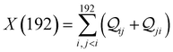 (magenta), and the total transmission from all MOs Z(192) = X(192) + Y(192) (red) for 2r circuit in the most thermally accessible conformation of TPm/p/o. Cumulative (magenta), and the total transmission from all MOs Z(192) = X(192) + Y(192) (red) for 2r circuit in the most thermally accessible conformation of TPm/p/o. Cumulative  plots and heatmaps for all TPo circuits are shown in ESI,† Fig. S11. (C) Orbitals that show highest DQI for the 2r circuit in the most thermally accessible conformation of TPo. The arrows show orbital phases (+/−) on terminal N-atoms (D)–(F) Basis circuit conductance (thermal averages and standard deviations) with REA (eqn (13)–(15)) for TPm and TPp based on three different models for estimating the effective screening length deff for the anchoring N-atoms as indicated in the panels (see also Methods Subsection 5.4). plots and heatmaps for all TPo circuits are shown in ESI,† Fig. S11. (C) Orbitals that show highest DQI for the 2r circuit in the most thermally accessible conformation of TPo. The arrows show orbital phases (+/−) on terminal N-atoms (D)–(F) Basis circuit conductance (thermal averages and standard deviations) with REA (eqn (13)–(15)) for TPm and TPp based on three different models for estimating the effective screening length deff for the anchoring N-atoms as indicated in the panels (see also Methods Subsection 5.4). | |
The  -factor analysis (Fig. 4B and ESI,† Fig. S11) on the most thermally accessible conformation of TPo shows that all basis circuits in the breadboard exhibit DQI (X(n = 192) < 0). Differing extents of DQI lead to variations in conductance within and across the breadboards (Fig. 4B and ESI,† Fig. S11). Cumulative pure MO contributions and orbital interference contributions add up such that the total current is higher for TPo relative to that of TPm (data for 2r circuits in Fig. 4B). Further, dominant conductance contributions arise from MOs 80–100 for TPo (region between the two black vertical lines in ESI,† Fig. S11). Visualizing the pure terms
  and QIE-induced contributions
  between orbital pairs for MOs 80–100, we find that there are only two dominant MOs (Fig. 4C) that interfere destructively leading to an overall DQI for the 2r circuit in TPo. Clearly, the DQI originates from the change in sign for the orbital amplitude on linking N-atoms (arrows in Fig. 4C).
Next, we examine the trends in conductance upon including REA (Fig. 4D) with deff estimated by eqn (10). The peripheral ortho placed N-atoms are less electrode accessible and the conformations of the terpyridine arm are more planar in the TPo breadboard (ESI,† Fig. S4E) relative to TPm (ESI,† Fig. S4D). These factors make both αp and αc in TPo significantly lower (Table 2) than in TPm. Interestingly, we find that REA suppresses the change in the relative basis circuit conductance induced by QIE (Fig. 4D). Overall, all basis circuits in TPo still have higher conductance than that of their counterparts in TPm even with REA. However, the boost in the basis circuit conductance for the former relative to the latter is lower than that in the absence of REA (compare Fig. 4D and A). As before, more restricted estimates of REA based on deff = 〈d(ϕ = 0)〉Th and 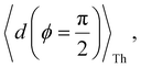 produce lower and upper bounds for the attenuation factors for TPo (Table 2). While only αc is reduced/increased for TPm, both αp and αc are reduced/increased for TPo. With deff = 〈d(ϕ = 0)〉Th, REA increases and each circuit (including 3rp) in TPo shows more than an order of magnitude higher conductance relative to their TPm counterparts (Fig. 4E). On the other hand, the overall effect of the reduced REA when
  is that the QIE-induced boost in conductance for TPo relative to TPm is completely nullified so that both breadboards show the same conductance trends (Fig. 4F).
3. Discussion
Over the past decade significant efforts are being made to develop functional molecular electronics. For instance, Joachim and co-workers have developed molecular logic gates using low temperature scanning tunneling microscopy and spectroscopy of starphene molecules on gold surfaces by manipulating the electrode–molecule interface.44,45 A molecular breadboard such as TPm presents an alternative framework to advance molecular electronics by assembling multiple electronic circuits (termed basis circuits) on a single scaffold. Combinations of these basis circuits (2r, 3rm, 3rp, 4r, and 5r) can be accessed in an experimental break-junction setup and mapped to distinct conductance readouts.24 Further, it is possible to change the electronic properties of individual constituent circuits of the breadboard using simple chemical changes accessible to synthetic chemists (this study). Finalized circuit designs can then be incorporated into stable covalently bonded single molecule junctions.46 Here, we present strategies to modify the relative conductance of the constituent basis circuits in TPx breadboards using the properties associated with the molecular structure (QIE) and the electrode–molecule interface (REA). Importantly, the computational framework presented here includes descriptions of both coherent and incoherent charge transport processes (ESI,† Section S10) and also rigorously accounts for the conformational flexibility of the molecular breadboard. In previous studies,33,38,40 QIE has been shown to modulate the conductance of conventional single molecule junctions by 1–2 orders of magnitude. Here, we demonstrate the presence of multi-orbital QIE in TPx breadboards associated with both ring connectivity and the placement of electrode-anchoring N-atoms. Differing extents of destructive QIE was found (Fig. 3A and 4A) to modulate the conductance of four basis circuits (2r, 3rm, 4r, and 5r) in TPx breadboards by ∼4–32-fold while holding the conductance of the reference 3rp circuit fixed (<2-fold variation). The second factor examined here—REA of the anchoring groups—is a molecule–electrode interface property. The spatial position of the electrode anchoring groups within a molecule can determine its accessibility (and hence the electronic coupling) to the electrode and can modulate basis circuit conductance. The relative conductance of basis circuits within a breadboard is thus decided by a combination of QIE and anchoring group REA. It is exciting to note that through chemical/molecular design, one can manipulate REA in a given breadboard scaffold to enhance, suppress, or leave unchanged any QIE induced changes in the relative basis circuit conductance. For instance, we demonstrated that by altering the N-atom position in the peripheral pyridyl rings from meta to para (TPm → TPp), we can hold REA of the anchoring N-atoms across two breadboards fixed and retain the pure QIE- induced boost in the relative circuit conductance (Fig. 3H–J). In contrast, by altering the peripheral pyridyl ring N-atom position from meta to ortho (TPm → TPo), the QIE-induced boosts may be partially or even completely suppressed because of the REA differences in the two breadboards (Fig. 4D–F). In essence, our studies indicate that QIE and REA are both useful to design and control the current flow through complex molecular electronic circuitry. In the future other electronic features sensitive to QIE such as current rectification47 and thermopower48,49 can be potentially targeted in breadboard junctions. However, one must be cognizant about the interdependence of tuning controls as discussed below.
In Fig. 5, we introduce phase plots to depict the changes in the conductance states of the basis circuits between two TPx breadboards in terms of the differences in 〈log(G/G0)〉 values (of the basis circuits) and the terminal N-atom REA (ξ from eqn (12)) ratios. We examine the changes in the basis circuit conductance relative to TPm as we switch either to TPp (Fig. 5A) or TPo (Fig. 5B). The range of ξ presented in the plot covers all the values observed in our calculations for the TPx systems. The phase plots in Fig. 5 are split into four quadrants (I, II, III, and IV) by a vertical black line at ξTPo/TPp = ξTPm (equal REA for the basis circuits in the two breadboards) and a horizontal black line at Δ〈log(G/G0)〉 = 0 (equal conductance for the basis circuits in the two breadboards). A point lying on the line ξTPo/TPp = ξTPm indicates that any changes in the basis circuit conductance have no REA contributions and are purely due to QIE. A point on the left (right) of the ξTPx = ξTPm line indicates suppression (enhancement) of the circuit conductance due to unequal REA of the anchoring N-atoms for a basis circuit in the two breadboards. A point lying on the Δ〈log(G/G0)〉 = 0 line indicates that the basis circuit conductance is unchanged in the two breadboards. This can happen either because the circuit is identical in the two breadboards or when QIE and REA oppose and balance each other. A point lying above (below) the Δ〈log(G/G0)〉 = 0 line indicates an increase (decrease) in the conductance for a basis circuit as we switch between the two breadboards. For data points lying in each of the four quadrants I, II, III, and IV, the conductance changes arise from a combination of QIE and REA. In general, such phase plots can help visualize the scope of tuning basis circuit conductance for any breadboard scaffold. For instance, we show changes in the conductance states of the five basis circuits for TPp and TPo breadboards relative to TPm in Fig. 5. All four scenarios presented in Results Subsection 2.2 (Fig. 3A and H–J) and Subsection 2.3 (Fig. 4A and D–F) are covered in the plots: (1) QIE in the absence of REA, (2) QIE + REA with deff estimated using eqn (10), (3) QIE + REA with deff = 〈d(ϕ = 0)〉Th, and (4) QIE + REA with 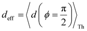 . We stress that Fig. 5A and B do not simply summarize the data in Fig. 3A, H–J and 4A, E–G but provide a broader perspective of the changes in the individual basis circuit conductance and the associated QIE/REA across the breadboard pairs. Specifically, in Fig. 3A, H–J and 4A, E–G, each conductance dataset is normalized with respect to the 3rp circuit conductance of TPm, whereas in Fig. 5, the conductance of each basis circuit is compared to its counterpart across two breadboards.
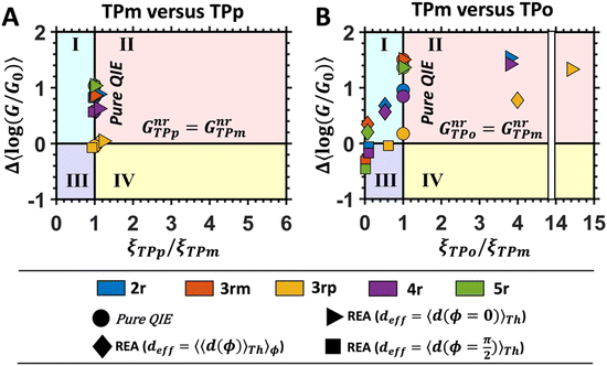 |
| | Fig. 5 Phase plot showing the difference in the mean logarithmic conductance of basis circuits in (A) TPp and TPm, and (B) TPo and TPm as a function of the ratio of REA (ξTPx/ξTPm) for the basis circuits. Here, Δ〈log(G/G0)〉 = 〈log(GnrTPx/G0)〉 − 〈log(GnrTPm/G0)〉, wherein x = p and o for panel (A) and (B), respectively. The four regions I, II, III, and IV demarcate the areas where QIE-induced boosts in the basis circuit conductance are either suppressed (I and III) or enhanced (II and IV) by REA and where QIE + REA either increases (I and II) or decreases (III and IV) the basis circuit conductance. A data point on ξTPx = ξTPm represents the change in circuit conductance across two breadboards purely due to QIE. A data point on the line Δ〈log(G/G0)〉 = 0 represents equal conductance of the basis circuits across the two breadboards. | |
Fig. 5A shows that pure QIE enhances (tunes) the conductance for four basis circuits (2r, 3rm, 4r, and 5r) to varying degrees in TPp relative to those in TPm. Here, 5r and 4r circuits exhibit the highest and lowest boosts in conductance, respectively (colored solid circles in Fig. 5A). 3rp circuit serves as a true reference, with no change in the conductance value, and lies at the intersection of the ξTPp = ξTPm and Δ〈log(G/G0)〉 = 0 lines (orange solid circle in Fig. 5A). This picture is preserved as REA is introduced (colored solid squares, triangles, and diamonds in Fig. 5A). For all four accessibility scenarios presented above, the changes in the conductance states for all basis circuits lie approximately on the ξTPp = ξTPm line and either above or approximately on the Δ〈log(G/G0)〉 = 0 line. This indicates that the conductance for all basis circuits (other than 3rp) in TPp is tuned purely due to QIE relative to that in TPm and that both breadboards have the same REA. On the other hand, the phase plot for TPo and TPm breadboards is far more complex. Fig. 5B shows that the changes in the conductance states for the basis circuits span three regions (I, II, and III) of the phase plot. Pure QIE enhances (tunes) the basis circuit conductance in TPo relative to that in TPm to varying degrees (solid circles on the ξTPo = ξTPm line in Fig. 5B) with the 3rm and 4r circuits showing the highest and lowest boosts, respectively. 3rp circuit, which has terminal core N-atoms, is unchanged in TPo and TPm and is used as a reference circuit in Fig. 4A, D–F as QIE effects are absent. However, we find that the conductance of the reference 3rp circuit in TPo is slightly higher (<2-fold) than that in TPm even in the absence of REA (orange solid circle in Fig. 5B). We attribute this difference to the higher conjugation in TPo molecule which adopts a more planar conformation relative to TPm (ESI,† Fig. S4D and E). While, the conformational effect is small in the present study, it is clear that significant differences in breadboard geometries may make it difficult to resolve conductance changes purely in terms of QIE and REA. In such cases a conformational coordinate axis may be added to the phase plots to better represent the data. When REA is included using deff = 〈〈d(ϕ)〉Th〉ϕ, the core N-atoms of TPo are more accessible to the electrodes than in TPm (Table 2) owing to the more planer geometries of the terpyridine arms (ESI,† Fig. S4E). Therefore, the change in conductance state of the 3rp circuit for this case lies deep in region II (orange solid diamond in Fig. 5B) arising purely due to REA differences. However, the accessibility of the peripheral N-atoms in TPo are lower than that in TPm, which places the conductance changes for the remaining 4 basis circuits in region I (colored solid diamonds in Fig. 5B). Overall, the QIE induced conductance boost of 2r, 3rm, 4r, and 5r circuits are all suppressed in TPo due to lower αp (and hence ξ) values for the basis circuits relative to those in TPm. On the other hand, the conductance change of the 3rp circuit in absence of REA (orange solid circle in Fig. 5B) is enhanced upon including REA due to a higher αc (and hence ξ) values in TPo relative to that in TPm arising from different conformations adopted by the two breadboards. For REA estimated with  , the restricted electrode–molecule interface makes both core and peripheral N-atoms in TPo less accessible to the electrode than in TPm (Table 2). In this case, the REA suppression of the circuit conductance in TPo relative to that in TPm is so large that it exceeds in magnitude the enhancements due to QIE. As a result, the changes in the conductance for 2r–5r circuits (colored solid squares in Fig. 5B) lie below the horizontal line Δ〈log(G/G0)〉 = 0. In contrast, REA with deff = 〈d(ϕ = 0)〉Th does not impact the QIE-induced enhancements for 3rm and 5r circuits, while further enhancing the QIE-induced boosts for 2r, 3rp, and 4r circuits owing to higher αc (and hence ξ) values in TPo relative to that in TPm. Thus, REA can both bolster (2r, 3rp, and 4r) or reverse (2r, 3rm, 4r, and 5r) the QIE-induced conductance changes of the basis circuits in TPo relative to those in TPm. The phase plots thus present a convenient framework to analyze the interdependence of QIE and REA in terms of controlling the basis circuit conductance within molecular breadboards.
4. Conclusions
We have presented a computational framework to design electronic molecular breadboards. The framework which accounts for both coherent and incoherent charge transport includes new advances in terms of an algorithm to efficiently sample molecular conformations, a molecule–electrode interface model to estimate REA of anchoring groups, and analysis of multi-orbital QIE, which should also be useful for the study of molecular junctions in general. Using this framework, we have computationally demonstrated the feasibility of altering the relative conductance of basis circuits (2r, 3rm, 3rp, 4r, and 5r) embedded within a bis-terpyridine molecular breadboard by repositioning the electrode anchoring N-atoms on each terpyridine arm. We show that the changes in the anchoring group placements translate into the changes in QIE and REA, which jointly modulate the basis circuit conductance in the bis-terpyridine breadboard. We demonstrate that QIE acting alone can potentially boost the conductance of four basis circuits in TPo and TPp relative to that in TPm by ∼ 4–32-fold, while preserving the conductance of the reference 3rp circuit across the three molecules. However, we predict that, in practice, REA differences for the anchoring N-atoms should suppress and maybe even reverse the expected QIE-induced enhancement in basis circuit conductance for TPo relative to TPm. In contrast, the QIE-induced boost in the basis circuit conductance of TPp relative to that of TPm is insensitive to REA.  -factor analysis reveals that the QIE is destructive for all basis circuits across the three breadboards. Finally, we introduced phase plots to visualize and analyze the interdependence of QIE and REA in modulating the changes in the basis circuit conductance. Beyond the application to TPx breadboards presented here, these plots provide a general framework to assess the scope of changes in other electronic properties of basis circuits such as rectification ratios and thermopower induced by chemical and physical changes to the molecular scaffold. We foresee that the introduction of an electrochemical gate37 can provide an exciting external control to enhance the scope of altering the basis circuit conductance in molecular breadboards. We envision that the computational framework presented here, in conjunction with break-junction experiments and the powerful toolkit of synthetic organic chemistry, will help in the design and development of more complex breadboards incorporating resistors, switches, diodes, transistors, and potentiometers as the constituent basis circuits.
5. Methods
5.1. Computational framework
We follow a methodology developed in group over the last decade which has been successful in describing charge transport in complex chemical systems with significant conformational flexibility including the bis-terpyridine breadboard.24,50–55 Our approach utilizes the full molecular Hamiltonian and enables us to explore multi-orbital contributions to charge transport and interference effects realistically. Here, we further extend our method to include a microscopic model of molecule–electrode coupling and introduce a new conformational sampling algorithm. These advances enable us to create a robust statistical description of molecular conductance which accounts for relative electrode accessibility of anchoring atoms and thermally weighted molecular conformations. We note that there exist several user-friendly and open source software packages to compute charge transport in molecules and materials such as TranSiesta56,57 and GOLLUM58 which could also potentially be used. However, our approach enables us examine charge transport more broadly beyond the few optimized molecular conformations and specific electrode morphologies (for example gold pyramids or hexagonal sheets) possible in existing software. While the packages also provide an option to input geometries sampled from molecular dynamics (MD). However, MD sampling is often limited to a local region of the molecular PES and also dependent on the availability of reliable force fields for molecules. Furthermore, a strategy to construct a statistical distribution of electrode geometries and their orientations with respect to molecule is missing in existing approaches. We hope that the methods introduced here for sampling thermally weighted molecular geometries and estimating molecule–electrode electronic couplings can be incorporated into these general user-friendly codes in the future.
5.2. Conformations of TPx (x = m, o, p) breadboards
In break-junction measurements the statistics is built by sampling over a thermal ensemble of molecular conformations. We therefore developed a general and transferable algorithm (ESI,† Section S1 and Fig. S1) to systematically enumerate molecular conformations and derive their thermal weight (see Results Subsection 2.1). In Section S1, we first demonstrate the algorithm by applying it to simpler molecules (ESI,† Fig. S2). Below we detail the enumeration of TPx breadboard conformations and the subsequent electronic structure calculations.
5.2.1. Enumeration of conformations for TPx breadboards.
For TPx breadboards, each of the six rotatable dihedrals (n = 6) shown in Fig. 6A assume four values (Qi = 4 ∀i∈ {1, 2,…, 6}; θi = 0°, 90°, 180°, and 270°) leading to a set (V) of  six-dimensional angle vectors (see Table 1). The TPx breadboards have three common molecular rotational symmetry matrices r1–r3 (eqn (S2)–(S4), ESI†) and two fragment rotational symmetries r4 and r5 (eqn (S5) and (S6), ESI†) associated with the terpyridine arms. The TPp molecule with para N-atoms has an additional symmetry matrix r6 (eqn (S7), ESI†) for peripheral rings. Eliminating redundant vectors from V using these symmetry elements and enantiomers gives 168, 168, and 23 distinct initial conformations for TPm, TPo, and TPp molecules respectively (see Table 1).
 |
| | Fig. 6 Schematic of TPm molecule with six rotatable dihedrals (θ1–θ6) attached to two microscopic electrodes. In our NEGF framework (Methods subsection 5.3), H is the electronic Hamiltonian and left (L) and right (R) electrodes are implicitly modeled in terms of their Fermi functions (fL/R) and coupling to the molecule ΓL/R (B) Schematic conformational energy landscape with initial set of enumerated conformations shown by vertical dotted lines. Upon geometry optimization, each such conformation relaxes to a local minimum (red arrows). (C) Schematic energy level diagram showing the electron/hole transport barriers (Δe/Δh) governing the charge transport across a molecular junction. The electrode electronic levels are governed by Fermi statistics and expressed in terms of the chemical potentials of left (μL) and right (μR) electrodes and their Fermi level (Ef). (D) Model for electrode–pyridyl attachment to calculate the screening distance (deff) for linking N-atoms that are not directly accessible to electrodes. The angle ϕ describes the tilt of the electrode plane relative to the plane of the pyridyl ring containing the N-atom of interest. Two extremes of the electrode approach (at ϕ= 0 and π/2) to the core N-atom where deff = dv and deff = dh. | |
Table 1 Enumeration of conformations of TPx breadboards. Here, n, Qi, and P are the number of rotatable dihedrals, number of values for ith dihedral torsion, and the total number of possible 6D angle vectors, respectively. D is the number of distinct initial conformations; Den is the number of distinct initial conformations after eliminating enantiomers; and Dopt is the number of final distinct optimized conformations after eliminating redundancies and enantiomers
| Molecule |
n
|
Q
i
|
P
|
D
|
D
|
D
en
|
D
opt
|
|
Symmetry matrices R are defined in ESI Section S1.
|
| TPm |
6 |
4,4,4,4,4,4 |
46 = 4096 |
r
1, r2, r3, r4, r5 |
288 |
168 |
69 |
| TPo |
6 |
4,4,4,4,4,4 |
46 = 4096 |
r
1, r2, r3, r4, r5 |
288 |
168 |
36 |
| TPp |
6 |
4,4,4,4,4,4 |
46 = 4096 |
r
1, r2, r3, r4, r5, r6 |
24 |
23 |
20 |
5.2.2. Geometry optimizations and electronic structure calculations.
Optimized geometries and their free energies (GF) were calculated for each initial conformation of the three TPx breadboards using density functional theory (DFT) with the B3LYP exchange–correlation (XC) functional and the 6-31G* basis set in Gaussian 09 revision D.01.59 During optimizations, conformations relaxed to local minima (red arrows in Fig. 6B). Based on the distribution of dihedrals (ESI,† Fig. S4), we grouped the optimized TPx conformations into clusters (ESI,† Fig. S1) using  where vk,vs ∈ V, k ≠ s and applying symmetry operations (Subsection 5.2.1 and ESI,† Section S1). Selecting one conformation from each cluster (Fig S5 of ESI†), we obtained 69, 36, and 20 geometrically distinct optimized conformations for TPm, TPo, and TPp, respectively (Table 1). For each of the distinct optimized breadboard geometries, semi-empirical INDO/s electronic structure calculations60 were carried out using the CNDO program61 to generate Hamiltonians which were used for subsequent charge transport calculations. There are a couple of reasons for not directly using a DFT Hamiltonian for our charge transport calculations. First, DFT with standard hybrid functionals is generally known to poorly describe charge transfer and underestimate the HOMO–LUMO gaps, resulting in the overestimation of the molecular conductance.62 This limitation can be overcome by using optimally-tuned range-separated hybrid functionals (OT-RSHs) which incorporate a distance-dependent mixing of Hartree–Fock exchange.62,63 However, in our case, this would imply deriving optimally tuned XC parameters which are consistent over a rather large number of thermally accessible breadboard geometries. Second, our molecule–electrode coupling parameters are introduced in the basis of atomic orbitals which is not straightforward to implement within a DFT framework. Although the INDO/s semi-empirical method overestimates HOMO–LUMO gaps, it is computationally cost effective and has proved effective in describing experimental data for the TPm breadboard.24
5.3. Charge transport calculations
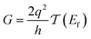
Conductance values for the five basis circuits (Fig. 1C), each embedded within 69, 36, and 20 geometrically distinct optimized conformations of TPm, TPo, and TPp, respectively, were calculated using the NEGF framework7,24 as:| | 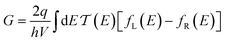 | (3) |
here q is electronic charge and h is the Planck constant. Fermi functions fL/R for the left (L) and right (R) electrodes with chemical potentials μL/R = Ef ± eV/2, where Ef and V are the Fermi energy and applied bias (Fig. 6C), are:| | 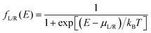 | (4) |
Here, kB is the Boltzmann constant and temperature T = 300 K. The transmission is:| | 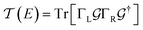 | (5) |
where,  is the molecular Green's function:
| |  | (6) |
Here, I is identity matrix, H is the INDO/s-generated molecular Hamiltonian in atomic basis, ΣL/R are complex self-energy contributions from left and right electrodes, with real shifts (neglected here) and imaginary broadenings (ΓL/R) of molecular energy levels. We adopt a model assuming that electrodes contact the molecules through N-atoms only:| |  | (7) |
where i and j run over the atomic orbitals, γ = 0.1 eV is the Au–N electronic coupling for an optimal coordination bond.24,51 The parameter α (estimated in Subsection 5.4 below) accounts for the REA of the anchoring N-atom and takes values between 0 (inaccessible to electrode) to 1 (full accessibility). It is a function of molecular conformation and represents the attenuation in electronic coupling as the Au–N coordination bond length increases beyond the optimal value. We assumed a small bias of V = 0.1 V with Fermi energy Ef = − 5.1 eV. Further, in our approach, incoherent transport contributions can also be included by incorporating phase-breaking probe electrodes (Landauer–Büttiker formulation) on specific molecular sites.53 An implementation of the Landauer–Büttiker framework for TPx breadboards is presented in ESI,† Section S9.
For TPx molecules, charge transport barriers (Δe = 4.4–4.8 eV and Δh = 2.8–3.3 eV in Fig. 6C) are large and transmission lengths are small (<2 nm). Ratner and coworkers64 found that for the barriers of 0.46 eV, incoherent hopping processes start dominating transport rates beyond transmission lengths of ∼1.4 nm which was consistent with experiments.65 Comparing the probability for tunneling (∝exp(−βd) with 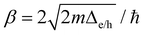 ) and thermally activated hopping
 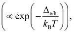 we estimate Gtunneling > 1030 × Gincoherent for all basis circuits in the three breadboards.64,66,67 For the longest (5r) circuit (1.03–1.76 nm), a barrier Δe/h ≤ 0.25 eV is required for incoherent transport to become competitive with tunneling transport. Consistent with our analysis, Xiang et al.66 recently fitted the experimental resistance versus distance data for DNA (transmission lengths of 1.4–3.2 nm) with competing hopping and tunneling mechanisms, estimating a barrier of ∼0.3 eV. Furthermore, explicit calculations on the TPx breadboards (ESI,† Fig. S17) and fits to experimental data on TPm (ESI,† Fig. S18) indicate that incoherent charge transport effects are insignificant. Thus, for the TPx molecules we assume that tunneling transport is exclusively operational.24,50,53 Within the small bias limit, eqn (3) is further simplified to:
| |  | (8) |
Using the eigen basis to express
H′ =
H + (
ΣL +
ΣR), the transmission can be decomposed as:
42| |  | (9) |
here, (°) represents the Hadamard product. The columns of

are the eigenvectors of
H′, termed conducting molecular orbitals (CMOs).
42 The diagonal elements

represent transmission contributions from the
ith CMO and are always real and positive

. The complex off-diagonal elements

represent the quantum interference between CMOs
i and
j. The total quantum interference

between
ith and
jth CMOs is always real as

and when non-zero its sign indicates either constructive

or destructive

interference. Here, we define multi-orbital quantum interference between
n CMOs as constructive (CQI) when

and destructive (DQI) when

. The manifestation of multi-orbital QIE for a simpler system
i.e., benzene can be demonstrated through

-factor analysis (see ESI,
† Section S6) and we apply it here to analyze conductance boosts/suppressions across the TP
x breadboards (Results subsections 2.2–2.3).
5.4. Electrode-pyridyl contact models for estimating α
The peripheral ring N-atoms in TPx breadboards are relatively more electrode accessible than the N-atoms in the core/central rings. Further, meta/para peripheral ring atoms are relatively more accessible to electrodes than ortho placed atoms. Previously,24 for the TPm breadboard, using a simple geometric model we estimated 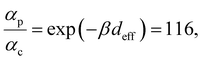 where deff is an effective screening length and β = 30 nm−1. Here, we develop a more general molecule–electrode interaction model which accounts for the REA of any pair of atoms across the three breadboards. Specifically, while the peripheral ring meta/para N-atoms are fully electrode accessible, the peripheral ortho N-atoms and core N-atoms have reduced accessibilities which depend on the molecular conformation (Fig. 6D). A lower accessibility of the breadboard N-atoms sterically constrains the Au–N coordination to larger-than-optimal bond length. Below, we estimate the Au–N bond extension beyond the optimal coordination for all N-atoms across the three breadboards.
We assume a planar electrode model interfacing with the TPx molecules over a range of tilt orientations (Fig. 6D) described by the angle ϕ between the normal vector to the electrode plane (![[n with combining right harpoon above (vector)]](https://www.rsc.org/images/entities/i_char_006e_20d1.gif) E) and that to a pyridyl ring plane (R). Assuming the van der Waal radius of Au ∼ 1.66 Å68 and formation of stable junctions α values are only estimated when an Au–N coordination bond is feasible. Based on solvent-accessible surface area calculations (ESI,† Fig. S15) we assume that the peripheral ring meta/para N-atoms can always form optimal coordination bonds (deff = 0 and α = 1 independent of ϕ). On the other hand, for the peripheral ring ortho N-atoms and the core ring N-atoms, the effective Au–N coordination length depends on ϕ (Fig. 6D and Table 2). Considering symmetry about the ring plane, we obtain the effective screening distance as:
E) and that to a pyridyl ring plane (R). Assuming the van der Waal radius of Au ∼ 1.66 Å68 and formation of stable junctions α values are only estimated when an Au–N coordination bond is feasible. Based on solvent-accessible surface area calculations (ESI,† Fig. S15) we assume that the peripheral ring meta/para N-atoms can always form optimal coordination bonds (deff = 0 and α = 1 independent of ϕ). On the other hand, for the peripheral ring ortho N-atoms and the core ring N-atoms, the effective Au–N coordination length depends on ϕ (Fig. 6D and Table 2). Considering symmetry about the ring plane, we obtain the effective screening distance as:
| |  | (10) |
here
d(
ϕ) is the distance of closest approach of the electrode plane to a linking N-atom (along the normal to the electrode plane) which is assumed to be uniformly distributed along
ϕ. Analytical expressions for
d(
ϕ) and estimates of thermally averaged attenuation factors for Au–N coordination across the breadboards are provided in
Table 2. For the two extreme angles,
ϕ = π/2 (orthogonal electrode and ring planes) and
ϕ = 0 (parallel electrode and ring planes), the electrode approach to the core ring N-atom is sterically hindered by the peripheral rings for non-planar breadboard geometries leading to screening distances
dh and
dv (
Fig. 6D), respectively. However, uniquely for TP
o which adopts nearly planar terpyridine arm geometries, both peripheral and core N-atoms in TP
o have restricted access to the electrode for
ϕ = π/2 while being fully accessible for
ϕ = 0 (see ESI,
† Fig. S4). Since the peripheral–core adjacent ring dihedrals (
θ) do not vary significantly across TP
x geometries, we averaged
θ first over all peripheral and core rings for a given conformation and then over all conformations in accordance with their thermal weight (〈
θ〉
Th = 22.8° /1.2° /21.1° for TP
m/
o/
p respectively). Further, in addition to
eqn (10), we also considered
deff = 〈
d(
ϕ = 0)〉
Th and
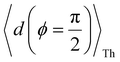
—corresponding to two extreme Au–N coordination geometries with the electrode plane parallel and orthogonal to the pyridyl ring plane respectively, as lower and upper bounds for the screening distance. Effective Au–N electronic couplings given by
eqn (7) were then estimated using
α = exp(−
βdeff) and with
β = 30 nm
−1 as the vacuum decay constant.
69 Using
eqn (10) we find
αp = 1 and
αc = 8.6 × 10
−3 for TP
m leading to a relative attenuation ratio

in agreement with our previous estimates in ref.
24. This model predicts slightly lower attenuation ratios

for TP
p and significantly lower ratios

for TP
o breadboards relative to that in TP
m. The REA estimation procedure developed here is transferrable to other systems as highlighted by its application to OPE molecules (ESI,
† Section S8) which are widely used in the study of single molecule junctions.
Table 2 Thermally averaged screening distances as a function of the tilt angle ϕ and the corresponding attenuation factors (α) for peripheral (p) and core (c) N-atoms in TPx breadboards. The distances dv/h are shown in Fig. 6D and b = 1.4 Å is the C–C bond length in the six-membered ring of TPx
| Molecule |
d(ϕ) for pa |
α
p
|
α
c
|
α
p
|
α
c
|
α
p
|
α
c
|
For core N-atom, d(ϕ) = 〈dv〉Th![[thin space (1/6-em)]](https://www.rsc.org/images/entities/char_2009.gif) cosϕ + 〈dh〉Thsinϕ is same for TPx breadboards. Averages are given by cosϕ + 〈dh〉Thsinϕ is same for TPx breadboards. Averages are given by 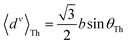 and and 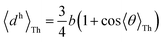 for core N-atoms in TPm/o/p, whereas only the ortho-placed peripheral N-atom (TPo) is screened with for core N-atoms in TPm/o/p, whereas only the ortho-placed peripheral N-atom (TPo) is screened with  and and  . Here, θ is the torsion angle between the peripheral and core rings.
Attenuation factors computed with . Here, θ is the torsion angle between the peripheral and core rings.
Attenuation factors computed with  . Here, the brackets 〈〉Th represent a thermal average in which the contribution of each conformation is multiplied by its Boltzmann weight. The brackets 〈〉ϕ represent an averaging over the tilt angle ϕ as given by eqn (10).
Attenuation factors computed with d = 〈d(ϕ = 0)〉Th.
Attenuation factors computed with . Here, the brackets 〈〉Th represent a thermal average in which the contribution of each conformation is multiplied by its Boltzmann weight. The brackets 〈〉ϕ represent an averaging over the tilt angle ϕ as given by eqn (10).
Attenuation factors computed with d = 〈d(ϕ = 0)〉Th.
Attenuation factors computed with  . .
|
| TPm |
0 |
1 |
8.6 × 10⁻³ |
1 |
0.24 |
1 |
2.4 × 10⁻³ |
| TPo |

|
0.26 |
1.7 × 10⁻² |
1 |
0.93 |
0.12 |
1.8 × 10⁻³ |
| TPp |
0 |
1 |
9.0 × 10⁻³ |
1 |
0.27 |
1 |
2.3 × 10⁻³ |
5.5. Statistical analysis of conductance
Within the weak coupling limit (Γii ≪ |E − Hii|), the transmission function (eqn (5)) for a basis circuit with the left electrode (L) connected to a peripheral/core N-atom (y = p/c) and the right electrode (R) connected to a peripheral/core N-atom (z = p/c) can be decomposed using eqn (7) as:| | 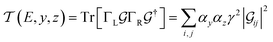 | (11) |
where indices i and j run over the orbitals connected to the L and R electrodes, respectively. Using eqn (8) and (11), conductance for a basis circuit within a specific breadboard conformation can be written as:| |  | (12) |
where  is a function of molecular conformation, and ξ = αyαz is a function of both molecule–electrode contacts and molecular conformation. Thus, we have:
| | | 〈log(G/G0)〉 = 〈log(K/G0)〉Th + 〈logξ〉Th | (13) |
Here the averages 〈log(K/G0)〉Th and 〈logξ〉 are over molecular conformations and the electrode–molecule interface heterogeneity, respectively. For a basis circuit in breadboard molecule B,| |  | (14) |
Here, index i runs over molecular conformations; wBi is the Boltzmann weight (eqn (1)) and Nnr is the multiplicity of a specific basis circuit in B (4 × 2r, 2 × 3rm, 1 × 3rp, 4 × 4r, and 4 × 5r). The index j runs from 1 to Nnr. Since αy and αz have an exponential form (Subsection 5.4) we have:| |  | (15) |
Here, β is the vacuum decay constant, and dy/zeff are effective screening lengths for peripheral or core N-atoms connected to L/R electrodes. The dy/zeff are thermally averaged over the torsion angles between the peripheral and core pyridyl rings. To summarize, we analyze the conductance of TPx in terms of thermal averages, given by eqn (13), and standard deviations as given by eqn (14) and (15) (raw data in Table S3, ESI†). We find σlogξ2 ≪ σlog(K/G0)2 for most of the circuits (except 2r and 3rp that have low σlog(K/G0)2) in TPx breadboards.
5.6. Model assumptions and caveats
Inelastic contributions70,71 arising from activation of vibrational degrees of freedom during charge transport are neglected as the charge tunneling time72 of ∼2 fs for a barrier of 2.8 eV over distances of ∼1.8 nm (lowest barrier and longest circuit in TPx) is much smaller than the fastest nuclear motions (60 fs to 20 ps). In fact, for the small values of applied bias (qV = 0.1 eV),73,74 the tunneling electron can activate only slower modes with time scales >260 fs. Furthermore, inelastic tunneling contributions even when present are expected to be much smaller (e.g. by more than an order of magnitude for benzenedithiol junctions) than that from elastic tunneling.70,73–75 Here, we neglect couplings of electrodes to N-atoms which are not part of the basis circuits when computing their conductance. We have shown previously24 that such couplings produce multi-terminal circuits whose conductance are determined by linear combinations of the irreducible set of five single terminal basis circuits (Fig. 1C) considered here. We have neglected correlated electron injection76 from electrode to molecule. While this might be relevant for TPo conformations with peripheral N-atoms pointing towards the core N-atoms, the Boltzmann populations for such conformations are insignificant. The electrode–molecule interface model presented here assumes a planar electrode. While electrode can take a multitude of shapes, its dimensions are much larger relative to the sub-nanometer molecular scale and the assumption of a planar electrode interface appears reasonable. Finally, solvent effects are neglected in our calculations. MCBJ experiments for TPm were conducted by us24 in organic solvent mixtures (1,3,5-trimethylbenzene (TMB) + tetrahydrofuran (THF) (4:1 v/v ratio)), and such solvents are not expected to influence the relative conductance trends examined here.
Author contributions
RK and RV designed research; RK performed research; RK, CS, VK, and RV analyzed data and wrote the paper.
Conflicts of interest
There are no conflicts to declare.
Acknowledgements
RK and RV acknowledge funding support from the Department of Atomic Energy (DAE), Government of India, under Project no. 12-R&D-TFR-5.10-0100. CS acknowledges funding from IoE-IISc postdoctoral fellowship and the N-PDF from SERB-DST. VK acknowledges the funding support from the Indian Institute of Science, DST-INSPIRE (DST/INSPIRE/04/2018/002983), SERB-Core research grant (CRG/2020/002302).
References
- M. Ratner, Nat. Nanotechnol., 2013, 8, 378–381 CrossRef CAS PubMed.
- N. Xin, J. Guan, C. Zhou, X. Chen, C. Gu, Y. Li, M. A. Ratner, A. Nitzan, J. F. Stoddart and X. Guo, Nat. Rev. Phys., 2019, 1, 211–230 CrossRef.
-
G. Cuniberti, G. Fagas and K. Richter, Introducing Molecular Electronics: A Brief Overview, Springer Berlin Heidelberg, Berlin, Heidelberg, 2005 Search PubMed.
- B. Xu and N. j Tao, Science, 2003, 301, 1221–1223 CrossRef CAS PubMed.
- L. Wang, L. Wang, L. Zhang and D. Xiang, Top. Curr. Chem., 2017, 375, 1–42 CrossRef CAS PubMed.
- C. Huang, A. V. Rudnev, W. Hong and T. Wandlowski, Chem. Soc. Rev., 2015, 44, 889–901 RSC.
-
S. Datta, Quantum Transport: Atom to Transistor, Cambridge University Press, 2005 Search PubMed.
- P. Moreno-García, M. Gulcur, D. Z. Manrique, T. Pope, W. Hong, V. Kaliginedi, C. Huang, A. S. Batsanov, M. R. Bryce, C. Lambert and T. Wandlowski, J. Am. Chem. Soc., 2013, 135, 12228–12240 CrossRef PubMed.
-
P. J. Low and S. Marqués-González, in Single-Molecule Electronics: An Introduction to Synthesis, Measurement and Theory, ed. M. Kiguchi, Springer Singapore, Singapore, 2016, pp. 87–116 Search PubMed.
- J. L. Zhang, J. Q. Zhong, J. D. Lin, W. P. Hu, K. Wu, G. Q. Xu, A. T. S. Wee and W. Chen, Chem. Soc. Rev., 2015, 44, 2998–3022 RSC.
- E. Lörtscher, J. W. Ciszek, J. Tour and H. Riel, Small, 2006, 2, 973–977 CrossRef PubMed.
- C. Wu, D. Bates, S. Sangtarash, N. Ferri, A. Thomas, S. J. Higgins, C. M. Robertson, R. J. Nichols, H. Sadeghi and A. Vezzoli, Nano Lett., 2020, 20, 7980–7986 CrossRef CAS PubMed.
- M. Elbing, R. Ochs, M. Koentopp, M. Fischer, C. Von Hänisch, F. Weigend, F. Evers, H. B. Weber and M. Mayor, Proc. Natl. Acad. Sci. U. S. A., 2005, 102, 8815–8820 CrossRef CAS PubMed.
- C. Van Dyck and M. A. Ratner, Nano Lett., 2015, 15, 1577–1584 CrossRef CAS PubMed.
- M. L. Perrin, E. Burzurí and H. S. J. Van Der Zant, Chem. Soc. Rev., 2015, 44, 902–919 RSC.
- S. Meisner, M. Kamenetska, M. Krikorian, M. L. Steigerwald, L. Venkataraman and C. Nuckolls, Nano Lett., 2011, 11, 1575–1579 CrossRef PubMed.
- F. L. Carter, Microelectron. Eng., 1984, 2, 11–24 CrossRef CAS.
-
M. Conrad, in Molecular Electronics: Biosensors and Biocomputers, ed. F. T. Hong, Springer US, Boston, MA, 1989, pp. 385–395 Search PubMed.
- V. Kaliginedi, A. V. Rudnev, P. Moreno-García, M. Baghernejad, C. Huang, W. Hong and T. Wandlowski, Phys. Chem. Chem. Phys., 2014, 16, 23529–23539 RSC.
- M. Magoga and C. Joachim, Phys. Rev. B: Condens. Matter Mater. Phys., 1999, 59, 16011–16021 CrossRef CAS.
- C. Joachim, J. K. Gimzewski and A. Aviram, Nature, 2000, 408, 541–548 CrossRef CAS PubMed.
- H. Vazquez, R. Skouta, S. Schneebeli, M. Kamenetska, R. Breslow, L. Venkataraman and M. S. Hybertsen, Nat. Nanotechnol., 2012, 7, 663–667 CrossRef CAS PubMed.
- K. C. Liao, L. Y. Hsu, C. M. Bowers, H. Rabitz and G. M. Whitesides, J. Am. Chem. Soc., 2015, 137, 5948–5954 CrossRef CAS PubMed.
- C. Seth, V. Kaliginedi, S. Suravarapu, D. Reber, W. Hong, T. Wandlowski, F. Lafolet, P. Broekmann, G. Royal and R. Venkatramani, Chem. Sci., 2017, 8, 1576–1591 RSC.
- M. Kiguchi, T. Ohto, S. Fujii, K. Sugiyasu, S. Nakajima, M. Takeuchi and H. Nakamura, J. Am. Chem. Soc., 2014, 136, 7327–7332 CrossRef CAS PubMed.
- M. Iwane, S. Fujii, T. Nishino and M. Kiguchi, J. Phys. Chem. C, 2016, 120, 8936–8940 CrossRef CAS.
- D. Miguel, L. Álvarez De Cienfuegos, A. Martín-Lasanta, S. P. Morcillo, L. A. Zotti, E. Leary, M. Bürkle, Y. Asai, R. Jurado, D. J. Cárdenas, G. Rubio-Bollinger, N. Agraït, J. M. Cuerva and M. T. González, J. Am. Chem. Soc., 2015, 137, 13818–13826 CrossRef CAS PubMed.
- Z. Li and E. Borguet, J. Am. Chem. Soc., 2012, 134, 63–66 CrossRef CAS PubMed.
- M. H. Garner, H. Li, Y. Chen, T. A. Su, Z. Shangguan, D. W. Paley, T. Liu, F. Ng, H. Li, S. Xiao, C. Nuckolls, L. Venkataraman and G. C. Solomon, Nature, 2018, 558, 416–419 CrossRef PubMed.
- V. Kaliginedi, P. Moreno-García, H. Valkenier, W. Hong, V. M. García-Suárez, P. Buiter, J. L. H. Otten, J. C. Hummelen, C. J. Lambert and T. Wandlowski, J. Am. Chem. Soc., 2012, 134, 5262–5275 CrossRef CAS PubMed.
- L. Venkataraman, J. E. Klare, C. Nuckolls, M. S. Hybertsen and M. L. Steigerwald, Nature, 2006, 442, 904–907 CrossRef CAS PubMed.
- W. Hong, D. Z. Manrique, P. Moreno-García, M. Gulcur, A. Mishchenko, C. J. Lambert, M. R. Bryce and T. Wandlowski, J. Am. Chem. Soc., 2012, 134, 2292–2304 CrossRef CAS PubMed.
- D. Z. Manrique, C. Huang, M. Baghernejad, X. Zhao, O. A. Al-Owaedi, H. Sadeghi, V. Kaliginedi, W. Hong, M. Gulcur, T. Wandlowski, M. R. Bryce and C. J. Lambert, Nat. Commun., 2015, 6, 6389 CrossRef CAS PubMed.
- T. A. Su, H. Li, M. L. Steigerwald, L. Venkataraman and C. Nuckolls, Nat. Chem., 2015, 7, 215–220 CrossRef CAS PubMed.
- C. Li, I. Pobelov, T. Wandlowski, A. Bagrets, A. Arnold and F. Evers, J. Am. Chem. Soc., 2008, 130, 318–326 CrossRef CAS PubMed.
- D. C. Milan, O. A. Al-Owaedi, M. C. Oerthel, S. Marqués-González, R. J. Brooke, M. R. Bryce, P. Cea, J. Ferrer, S. J. Higgins, C. J. Lambert, P. J. Low, D. Z. Manrique, S. Martin, R. J. Nichols, W. Schwarzacher and V. M. García-Suárez, J. Phys. Chem. C, 2016, 120, 15666–15674 CrossRef CAS.
- Y. Li, M. Buerkle, G. Li, A. Rostamian, H. Wang, Z. Wang, D. R. Bowler, T. Miyazaki, L. Xiang, Y. Asai, G. Zhou and N. Tao, Nat. Mater., 2019, 18, 357–364 CrossRef CAS PubMed.
- C. R. Arroyo, S. Tarkuc, R. Frisenda, J. S. Seldenthuis, C. H. M. Woerde, R. Eelkema, F. C. Grozema and H. S. J. Van Der Zant, Angew. Chem., Int. Ed., 2013, 52, 3152–3155 CrossRef CAS PubMed.
- T. Markussen, R. Stadler and K. S. Thygesen, Nano Lett., 2010, 10, 4260–4265 CrossRef CAS PubMed.
- M. G. Reuter and T. Hansen, J. Chem. Phys., 2014, 141, 181103 CrossRef PubMed.
- P. Sam-Ang and M. G. Reuter, New J. Phys., 2017, 19, 53002 CrossRef.
- S. Gunasekaran, J. E. Greenwald and L. Venkataraman, Nano Lett., 2020, 20, 2843–2848 CrossRef CAS PubMed.
- F. Jiang, D. I. Trupp, N. Algethami, H. Zheng, W. He, A. Alqorashi, C. Zhu, C. Tang, R. Li, J. Liu, H. Sadeghi, J. Shi, R. Davidson, M. Korb, A. N. Sobolev, M. Naher, S. Sangtarash, P. J. Low, W. Hong and C. J. Lambert, Angew. Chem., Int. Ed., 2019, 58, 18987–18993 CrossRef CAS PubMed.
- D. Skidin, O. Faizy, J. Krüger, F. Eisenhut, A. Jancarik, K. H. Nguyen, G. Cuniberti, A. Gourdon, F. Moresco and C. Joachim, ACS Nano, 2018, 12, 1139–1145 CrossRef CAS PubMed.
- W. H. Soe, P. De Mendoza, A. M. Echavarren and C. Joachim, J. Phys. Chem. Lett., 2021, 12, 8528–8532 CrossRef CAS PubMed.
- C. Jia, A. Migliore, N. Xin, S. Huang, J. Wang, Q. Yang, S. Wang, H. Chen, D. Wang, B. Feng, Z. Liu, G. Zhang, D. H. Qu, H. Tian, M. A. Ratner, H. Q. Xu, A. Nitzan and X. Guo, Science, 2016, 352, 1443–1445 CrossRef CAS PubMed.
- A. Polakovsky, J. Showman, J. Valdiviezo and J. L. Palma, Phys. Chem. Chem. Phys., 2021, 23, 1550–1557 RSC.
- J. P. Bergfield, M. A. Solis and C. A. Stafford, ACS Nano, 2010, 4, 5314–5320 CrossRef CAS PubMed.
- R. Miao, H. Xu, M. Skripnik, L. Cui, K. Wang, K. G. L. Pedersen, M. Leijnse, F. Pauly, K. Wärnmark, E. Meyhofer, P. Reddy and H. Linke, Nano Lett., 2018, 18, 5666–5672 CrossRef CAS PubMed.
- A. Paul, E. Wierzbinski, D. H. Waldeck, S. Bezer, L. Kocsis, C. Achim, R. Venkatramani, A. Balaeff, S. Keinan and D. N. Beratan, J. Am. Chem. Soc., 2009, 131, 6498–6507 CrossRef CAS PubMed.
- Y. Xing, T. H. Park, R. Venkatramani, S. Keinan, D. N. Beratan, M. J. Therien and E. Borguet, J. Am. Chem. Soc., 2010, 132, 7946–7956 CrossRef CAS PubMed.
- R. Venkatramani, K. L. Davis, E. Wierzbinski, S. Bezer, A. Balaeff, S. Keinan, A. Paul, L. Kocsis, D. N. Beratan, C. Achim and D. H. Waldeck, J. Am. Chem. Soc., 2011, 133, 62–72 CrossRef CAS PubMed.
- R. Venkatramani, E. Wierzbinski, D. H. Waldeck and D. N. Beratan, Faraday Discuss., 2014, 174, 57–78 RSC.
- A. Aggarwal, S. Bag, R. Venkatramani, M. Jain and P. K. Maiti, Nanoscale, 2020, 12, 18750–18760 RSC.
- R. Kumar, C. Seth, R. Venkatramani and V. Kaliginedi, Nanoscale, 2023, 15, 15050–15058 RSC.
- N. Papior, N. Lorente, T. Frederiksen, A. García and M. Brandbyge, Comput. Phys. Commun., 2017, 212, 8–24 CrossRef CAS.
- M. Brandbyge, J. L. Mozos, P. Ordejón, J. Taylor and K. Stokbro, Phys. Rev. B: Condens. Matter Mater. Phys., 2002, 65, 165401 CrossRef.
- J. Ferrer, C. J. Lambert, V. M. García-Suárez, D. Z. Manrique, D. Visontai, L. Oroszlany, R. Rodríguez-Ferradás, I. Grace, S. W. D. Bailey, K. Gillemot, H. Sadeghi and L. A. Algharagholy, New J. Phys., 2014, 16, 093029 CrossRef.
-
M. J. Frisch, G. W. Trucks, H. B. Schlegel, G. E. Scuseria, M. A. Robb, J. R. Cheeseman, G. Scalmani, V. Barone, B. Mennucci, G. A. Petersson, H. Nakatsuji, M. Caricato, X. Li, H. P. Hratchian, A. F. Izmaylov, J. Bloino, G. Zheng, J. L. Sonnenberg, M. Hada, M. Ehara, K. Toyota, R. Fukuda, J. Hasegawa, M. Ishida, T. Nakajima, Y. Honda, O. Kitao, H. Nakai, T. Vreven, J. A. Montgomery Jr., J. E. Peralta, F. Ogliaro, M. Bearpark, J. J. Heyd, E. Brothers, K. N. Kudin, V. N. Staroverov, T. Keith, R. Kobayashi, J. Normand, K. Raghavachari, A. Rendell, J. C. Burant, S. S. Iyengar, J. Tomasi, M. Cossi, N. Rega, J. M. Millam, M. Klene, J. E. Knox, J. B. Cross, V. Bakken, C. Adamo, J. Jaramillo, R. Gomperts, R. E. Stratmann, O. Yazyev, A. J. Austin, R. Cammi, C. Pomelli, J. W. Ochterski, R. L. Martin, K. Morokuma, V. G. Zakrzewski, G. A. Voth, P. Salvador, J. J. Dannenberg, S. Dapprich, A. D. Daniels, Ö. Farkas, J. B. Foresman, J. V. Ortiz, J. Cioslowski and D. J. Fox, Gaussian 09, revision D.01, Gaussian Inc. Wallingford, 2013 Search PubMed.
- J. Ridley and M. Zerner, Thoret. chim. Acta, 1973, 32, 111–134 CrossRef CAS.
- J. Zeng, N. S. Hush and J. R. Reimers, J. Am. Chem. Soc., 1996, 118, 2059–2068 CrossRef CAS.
- Z. F. Liu, S. Wei, H. Yoon, O. Adak, I. Ponce, Y. Jiang, W. D. Jang, L. M. Campos, L. Venkataraman and J. B. Neaton, Nano Lett., 2014, 14, 5365–5370 CrossRef CAS PubMed.
- B. M. Wong and T. H. Hsieh, J. Chem. Theory Comput., 2010, 6, 3704–3712 CrossRef CAS PubMed.
- Y. A. Berlin, A. L. Burin and M. A. Ratner, Chem. Phys., 2002, 275, 61–74 CrossRef CAS.
- B. Giese, J. Amaudrut, A. K. Köhler, M. Spormann and S. Wessely, Nature, 2001, 412, 318–320 CrossRef CAS PubMed.
- L. Xiang, J. L. Palma, C. Bruot, V. Mujica, M. A. Ratner and N. Tao, Nat. Chem., 2015, 7, 221–226 CrossRef CAS PubMed.
- S. H. Choi, B. Kim and F. C. Daniel, Science, 2008, 320, 1482–1486 CrossRef CAS PubMed.
- A. Bondi, J. Phys. Chem., 1964, 68, 441–451 CrossRef CAS.
- L. Mejía, N. Renaud and I. Franco, J. Phys. Chem. Lett., 2018, 9, 745–750 CrossRef PubMed.
- M. Galperin, M. A. Ratner and A. Nitzan, J. Chem. Phys., 2004, 121, 11965–11979 CrossRef CAS PubMed.
- J. Liu and D. Segal, Phys. Rev. B, 2020, 101, 155406 CrossRef CAS.
- A. Nitzan, J. Jortner, J. Wilkie, A. L. Burin and M. A. Ratner, J. Phys. Chem. B, 2000, 104, 5661–5665 CrossRef CAS.
- M. Tsutsui and M. Taniguchi, J. Appl. Phys., 2013, 113, 084301 CrossRef.
- S. You, J. T. Lü, J. Guo and Y. Jiang, Adv. Phys. X, 2017, 2, 907–936 CAS.
- M. Thoss and F. Evers, J. Chem. Phys., 2018, 148, 030901 CrossRef PubMed.
- A. D. Levine and U. Peskin, Mol. Phys., 2019, 117, 2097–2107 CrossRef CAS.
|
| This journal is © The Royal Society of Chemistry 2023 |

 b and
Ravindra
Venkatramani
b and
Ravindra
Venkatramani
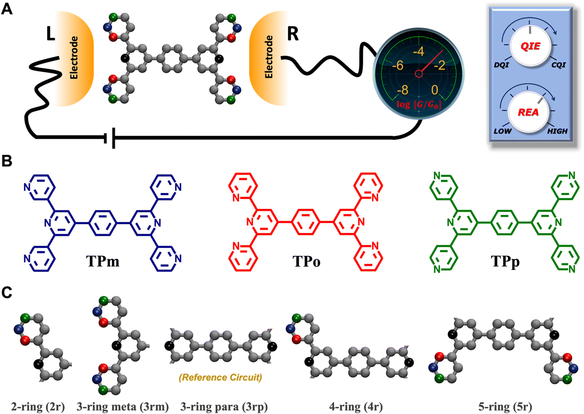
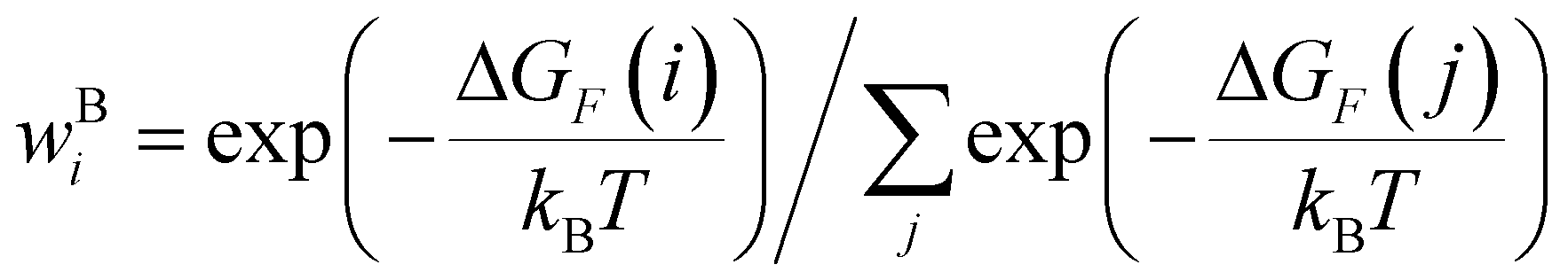
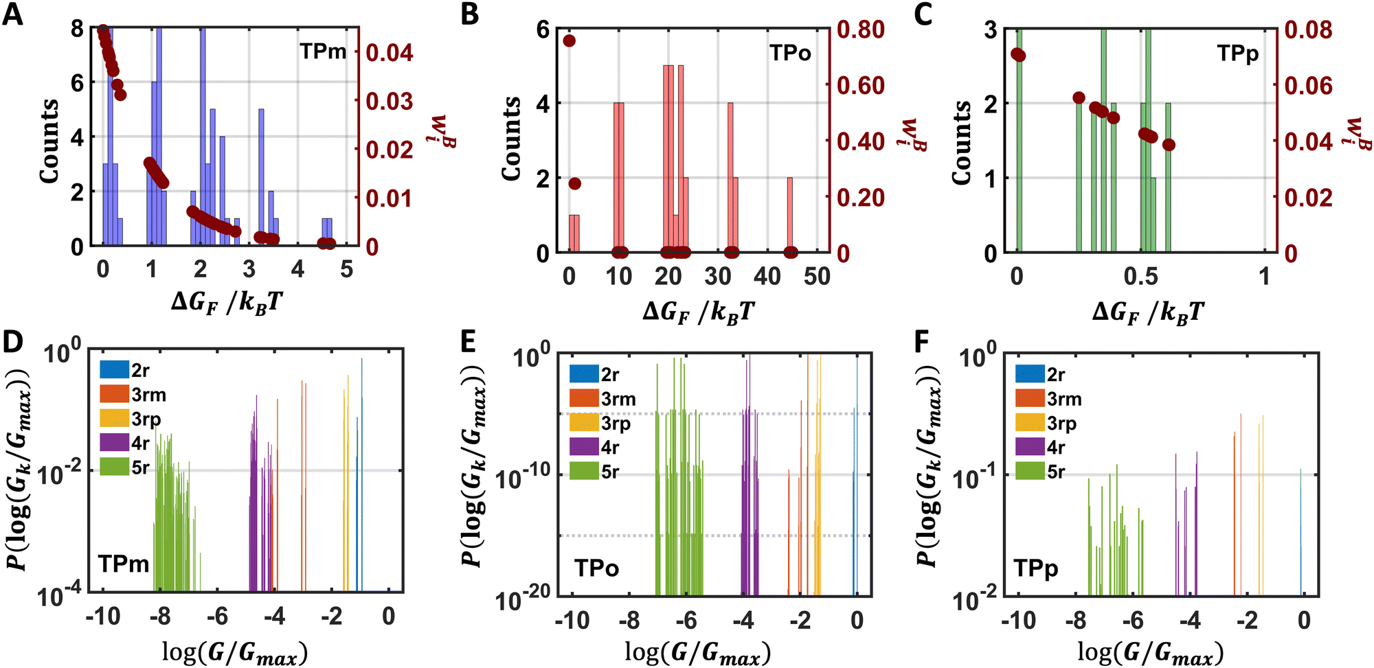

 . Here, index i runs over all the distinct geometries of B; x is the number of n-ring circuits in the breadboard conformation i with conductance values lying in the bin centered at log(Gk/Gmax); Nnr is the multiplicity of an n-ring circuit (4 × 2r, 2 × 3rm, 1 × 3rp, 4 × 4r, and 4 × 5r) in the TPx scaffold. The multiple conductance peaks for each circuit in the three breadboards (Fig. 2D–F) arise from heterogeneities in the thermally accessible molecular conformations (see ESI,† Section S4 for details). Further, within each breadboard, the conductance distributions for the basis circuits are roughly ordered by the end-to-end circuit length (2r > 3rm > 3rp > 4r > 5r) with a single exception (G3rp > G3rm). Further, comparing the breadboards, the basis circuit conductance (excluding the invariant 3rp circuit) in TPm is lower than that for circuits in TPo (Fig. 2D and E) and in TPp (Fig. 2D and F). The lower conductance of the 3rm circuit relative to 3rp and the relative conductance trends for corresponding basis circuits across the three breadboards is in accordance with the quantum circuit rules demonstrated by Manrique et al. for OPE-based molecules.33 Essentially, a meta-placement of the peripheral pyridyl N-atoms and meta ring connectivity both lower conductance relative to the corresponding molecules with para/ortho N-atom placement and para-ring connectivity. While the differences in the breadboard conformations could also potentially contribute, we show in the following subsections that these conductance trends are primarily due to QIE.

 -matrix elements: Pure contributions from MOs
  (cyan), QI contributions
  (magenta), and the overall cumulative transmission Z(n) = X(n) + Y(n) (blue/green for TPm/p respectively) for 2r circuit in the most thermally accessible conformation of TPm and TPp. Data for other circuits is shown in ESI,† Fig. S11. (D) and (E) Heatmap showing
  -matrix elements for dominant MOs (80–100) representing pure orbital contributions and interference contributions between pair of MOs for TPm and TPp. Heatmap for all orbitals are provided in ESI,† Fig. S12 and S13 (F)–(G) Orbitals that show highest DQI for the 2r circuit in the most thermally accessible conformation of TPm and TPp. The arrows show orbital phases (+/−) on terminal N-atoms (H)–(J) Basis circuit conductance (thermal averages and standard deviations) with REA (eqn (13)–(15)) for TPm and TPp based on three different models for estimating the effective screening length deff for the anchoring N-atoms as indicated in the panels (see also Methods Subsection 5.4).
 -factor analysis (Methods Subsection 5.3 and ESI,† Section 6) we show that all the basis circuits in the TPm and TPp breadboards exhibit destructive multi-orbital quantum interference (DQI) and attribute the variations in conductance within and across the breadboards to the differing extents of DQI. In Fig. 3B and C, we present data for the most thermally accessible (highest wBi) conformations of 2r in TPm and TPp breadboards (ESI,† Fig. S11 shows data for other basis circuits). Fig. 3B shows cumulative diagonal (pure contributions Y) and off-diagonal (quantum interference contributions X) elements of the
  -matrix along with their sum (the transmission Z) for TPm as a function of orbital index (n). The corresponding data for TPp is presented in Fig. 3C. While the total transmission from all MOs (Z(n = 192)) for the 2r circuit in TPp is higher than that in TPm, it is apparent that 2r circuits in both breadboards show DQI (X(n = 192) < 0 in Fig. 3B and C). In fact, all five basis circuits in TPm and TPp exhibit DQI (ESI,† Fig. S11). However, the DQI is lower for all circuits in TPp relative to those in TPm leading to the observed differences in conductance values (Fig. 3A). Further, the quantum interference is clearly multi-orbital in nature. For instance, strong conductance contributions arise from MOs 80–100 and MOs 80–130 for 2r in TPm and TPp respectively (data between the two black vertical lines in Fig. 3B and C). A decomposition of the pure
  and quantum interference contributions
  for dominant MOs 80–100 of the 2r circuit shows (Fig. 3D and E) that while contributions from MO pairs interfere both destructively and constructively, the total interference from dominant MOs is DQI. In Fig. 3F and G, we visualize MO pairs with the highest DQI for the 2r circuit in TPm and TPp respectively. The DQI originates from the differences in signs of orbital amplitudes at the terminal N-atoms (arrows in Fig. 3F and G).
 produce lower and upper bounds for αc leaving αp unchanged (Table 2). The conductance of basis circuits for REA with deff = 〈d(ϕ = 0)〉Th are close to pure QIE trends (compare Fig. 3I and A). On the other hand, REA with
  alters the relative conductance trends across the five basis circuits within each breadboard (compare Fig. 3H and J). Nevertheless, the relative boosts in the basis circuit conductance between TPp and TPm produced by QIE are still preserved with the new REA estimates since both αp and αc for the two breadboards remain comparable.
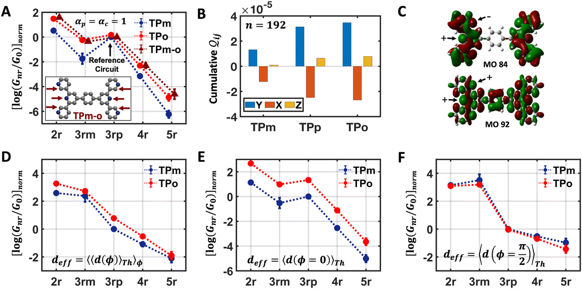
 -matrix elements: Sum of pure contributions from all MOs
 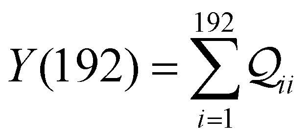 (cyan), QI contributions
 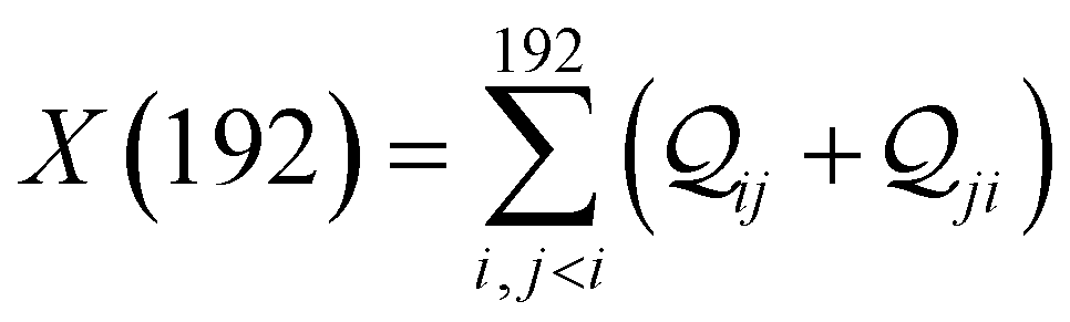 (magenta), and the total transmission from all MOs Z(192) = X(192) + Y(192) (red) for 2r circuit in the most thermally accessible conformation of TPm/p/o. Cumulative
 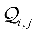 plots and heatmaps for all TPo circuits are shown in ESI,† Fig. S11. (C) Orbitals that show highest DQI for the 2r circuit in the most thermally accessible conformation of TPo. The arrows show orbital phases (+/−) on terminal N-atoms (D)–(F) Basis circuit conductance (thermal averages and standard deviations) with REA (eqn (13)–(15)) for TPm and TPp based on three different models for estimating the effective screening length deff for the anchoring N-atoms as indicated in the panels (see also Methods Subsection 5.4).
 -factor analysis (Fig. 4B and ESI,† Fig. S11) on the most thermally accessible conformation of TPo shows that all basis circuits in the breadboard exhibit DQI (X(n = 192) < 0). Differing extents of DQI lead to variations in conductance within and across the breadboards (Fig. 4B and ESI,† Fig. S11). Cumulative pure MO contributions and orbital interference contributions add up such that the total current is higher for TPo relative to that of TPm (data for 2r circuits in Fig. 4B). Further, dominant conductance contributions arise from MOs 80–100 for TPo (region between the two black vertical lines in ESI,† Fig. S11). Visualizing the pure terms
  and QIE-induced contributions
 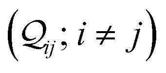 between orbital pairs for MOs 80–100, we find that there are only two dominant MOs (Fig. 4C) that interfere destructively leading to an overall DQI for the 2r circuit in TPo. Clearly, the DQI originates from the change in sign for the orbital amplitude on linking N-atoms (arrows in Fig. 4C).
 produce lower and upper bounds for the attenuation factors for TPo (Table 2). While only αc is reduced/increased for TPm, both αp and αc are reduced/increased for TPo. With deff = 〈d(ϕ = 0)〉Th, REA increases and each circuit (including 3rp) in TPo shows more than an order of magnitude higher conductance relative to their TPm counterparts (Fig. 4E). On the other hand, the overall effect of the reduced REA when
  is that the QIE-induced boost in conductance for TPo relative to TPm is completely nullified so that both breadboards show the same conductance trends (Fig. 4F).
 . We stress that Fig. 5A and B do not simply summarize the data in Fig. 3A, H–J and 4A, E–G but provide a broader perspective of the changes in the individual basis circuit conductance and the associated QIE/REA across the breadboard pairs. Specifically, in Fig. 3A, H–J and 4A, E–G, each conductance dataset is normalized with respect to the 3rp circuit conductance of TPm, whereas in Fig. 5, the conductance of each basis circuit is compared to its counterpart across two breadboards.
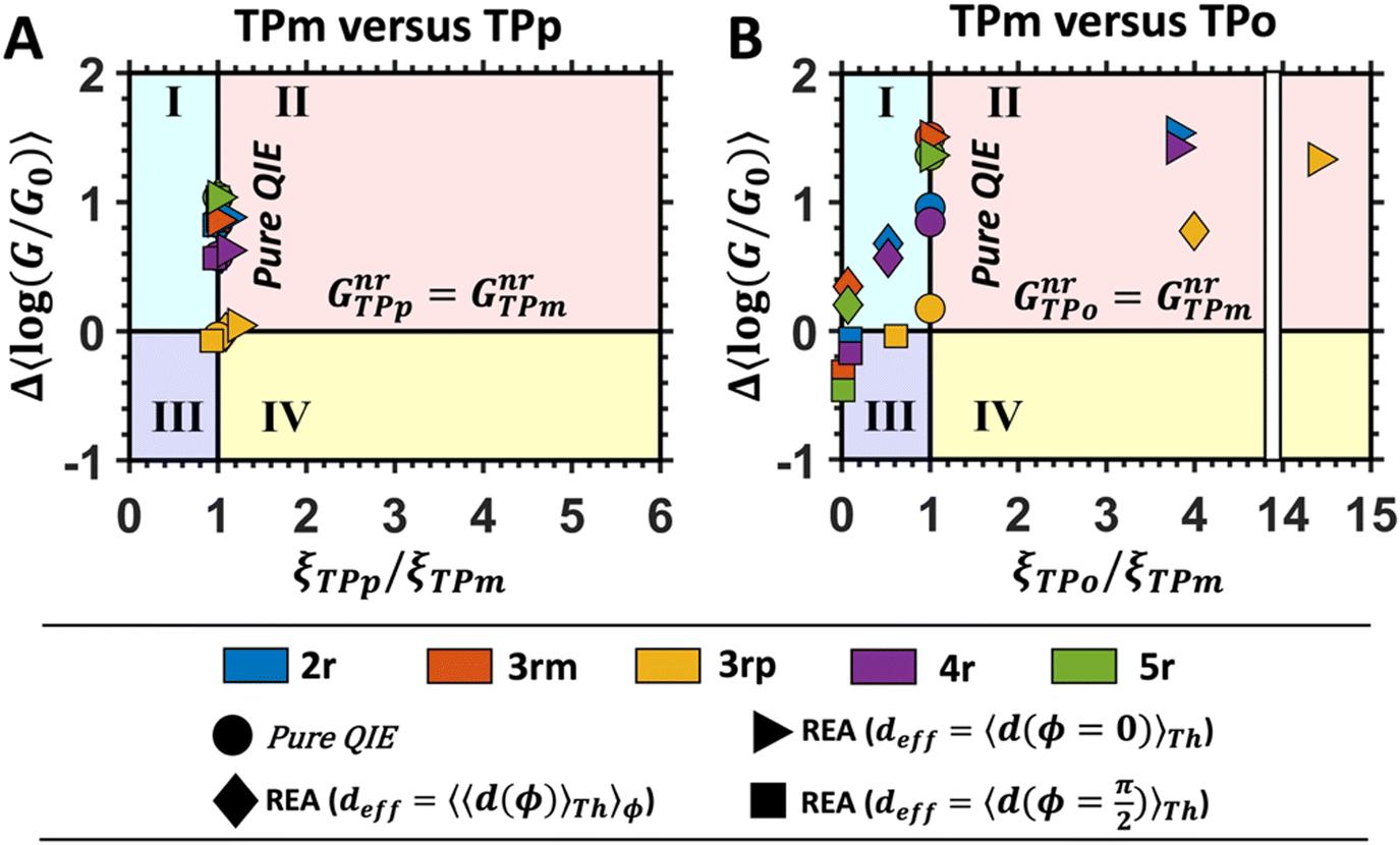
 , the restricted electrode–molecule interface makes both core and peripheral N-atoms in TPo less accessible to the electrode than in TPm (Table 2). In this case, the REA suppression of the circuit conductance in TPo relative to that in TPm is so large that it exceeds in magnitude the enhancements due to QIE. As a result, the changes in the conductance for 2r–5r circuits (colored solid squares in Fig. 5B) lie below the horizontal line Δ〈log(G/G0)〉 = 0. In contrast, REA with deff = 〈d(ϕ = 0)〉Th does not impact the QIE-induced enhancements for 3rm and 5r circuits, while further enhancing the QIE-induced boosts for 2r, 3rp, and 4r circuits owing to higher αc (and hence ξ) values in TPo relative to that in TPm. Thus, REA can both bolster (2r, 3rp, and 4r) or reverse (2r, 3rm, 4r, and 5r) the QIE-induced conductance changes of the basis circuits in TPo relative to those in TPm. The phase plots thus present a convenient framework to analyze the interdependence of QIE and REA in terms of controlling the basis circuit conductance within molecular breadboards.
 -factor analysis reveals that the QIE is destructive for all basis circuits across the three breadboards. Finally, we introduced phase plots to visualize and analyze the interdependence of QIE and REA in modulating the changes in the basis circuit conductance. Beyond the application to TPx breadboards presented here, these plots provide a general framework to assess the scope of changes in other electronic properties of basis circuits such as rectification ratios and thermopower induced by chemical and physical changes to the molecular scaffold. We foresee that the introduction of an electrochemical gate37 can provide an exciting external control to enhance the scope of altering the basis circuit conductance in molecular breadboards. We envision that the computational framework presented here, in conjunction with break-junction experiments and the powerful toolkit of synthetic organic chemistry, will help in the design and development of more complex breadboards incorporating resistors, switches, diodes, transistors, and potentiometers as the constituent basis circuits.
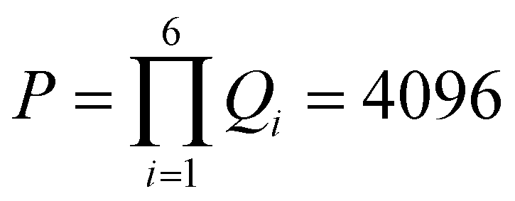 six-dimensional angle vectors (see Table 1). The TPx breadboards have three common molecular rotational symmetry matrices r1–r3 (eqn (S2)–(S4), ESI†) and two fragment rotational symmetries r4 and r5 (eqn (S5) and (S6), ESI†) associated with the terpyridine arms. The TPp molecule with para N-atoms has an additional symmetry matrix r6 (eqn (S7), ESI†) for peripheral rings. Eliminating redundant vectors from V using these symmetry elements and enantiomers gives 168, 168, and 23 distinct initial conformations for TPm, TPo, and TPp molecules respectively (see Table 1).
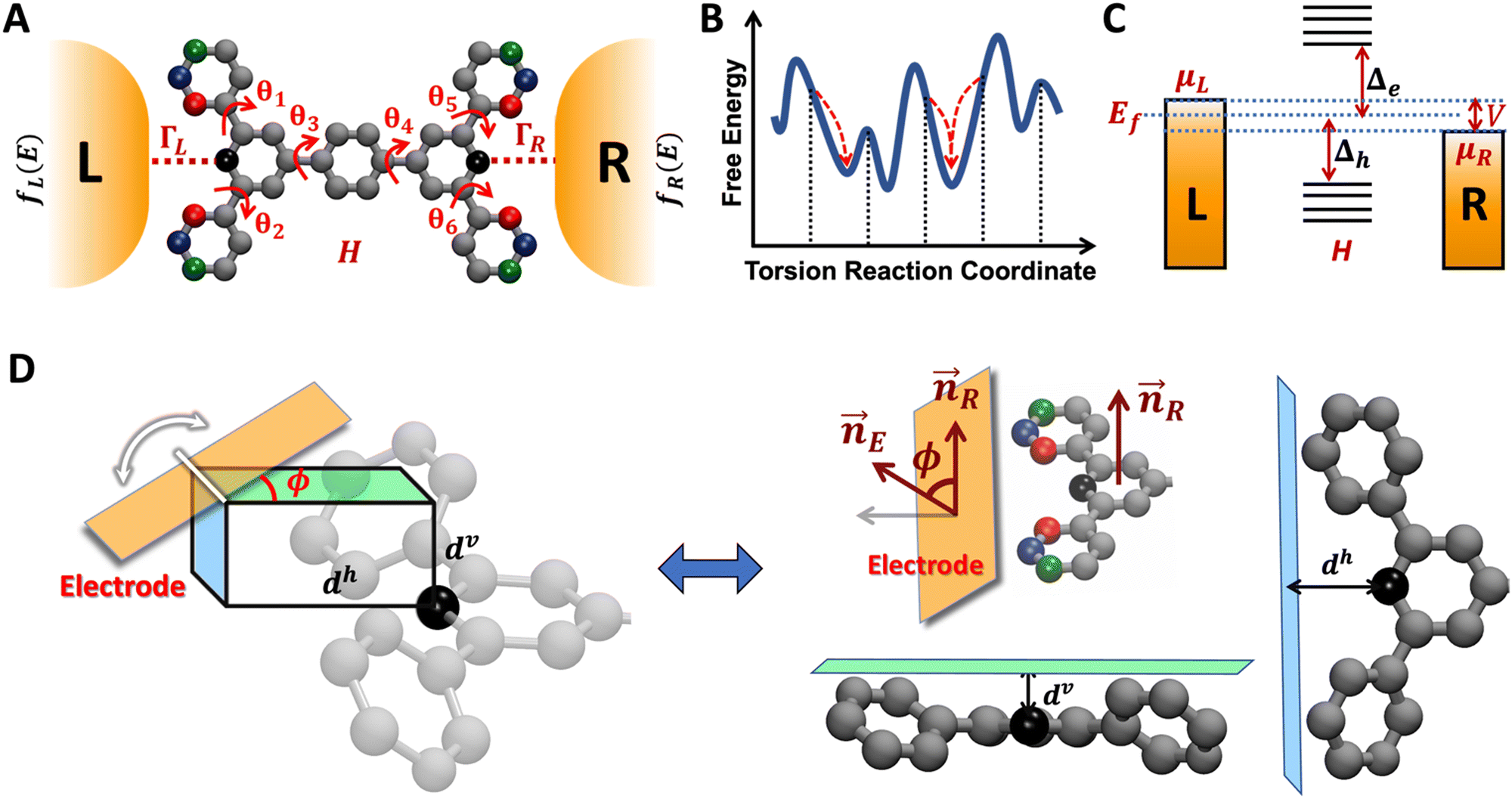
 where vk,vs ∈ V, k ≠ s and applying symmetry operations (Subsection 5.2.1 and ESI,† Section S1). Selecting one conformation from each cluster (Fig S5 of ESI†), we obtained 69, 36, and 20 geometrically distinct optimized conformations for TPm, TPo, and TPp, respectively (Table 1). For each of the distinct optimized breadboard geometries, semi-empirical INDO/s electronic structure calculations60 were carried out using the CNDO program61 to generate Hamiltonians which were used for subsequent charge transport calculations. There are a couple of reasons for not directly using a DFT Hamiltonian for our charge transport calculations. First, DFT with standard hybrid functionals is generally known to poorly describe charge transfer and underestimate the HOMO–LUMO gaps, resulting in the overestimation of the molecular conductance.62 This limitation can be overcome by using optimally-tuned range-separated hybrid functionals (OT-RSHs) which incorporate a distance-dependent mixing of Hartree–Fock exchange.62,63 However, in our case, this would imply deriving optimally tuned XC parameters which are consistent over a rather large number of thermally accessible breadboard geometries. Second, our molecule–electrode coupling parameters are introduced in the basis of atomic orbitals which is not straightforward to implement within a DFT framework. Although the INDO/s semi-empirical method overestimates HOMO–LUMO gaps, it is computationally cost effective and has proved effective in describing experimental data for the TPm breadboard.24
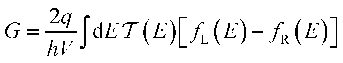

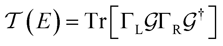
 is the molecular Green's function:
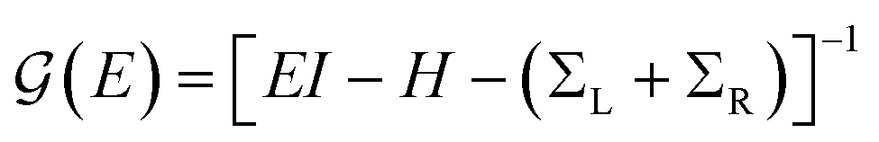
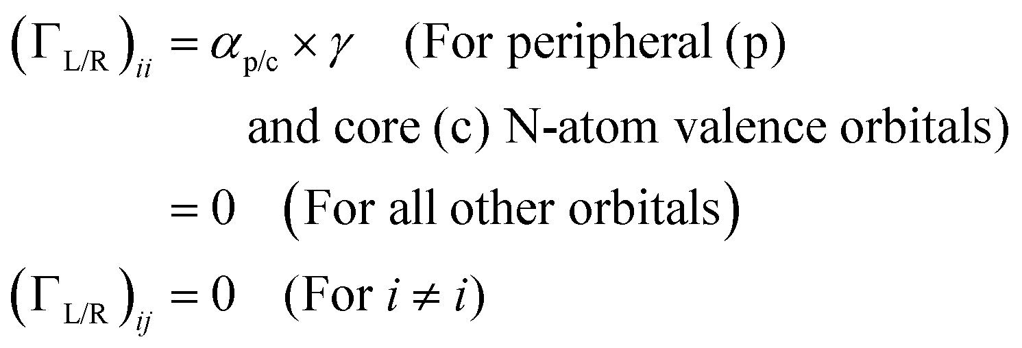
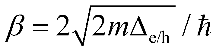 ) and thermally activated hopping
  we estimate Gtunneling > 1030 × Gincoherent for all basis circuits in the three breadboards.64,66,67 For the longest (5r) circuit (1.03–1.76 nm), a barrier Δe/h ≤ 0.25 eV is required for incoherent transport to become competitive with tunneling transport. Consistent with our analysis, Xiang et al.66 recently fitted the experimental resistance versus distance data for DNA (transmission lengths of 1.4–3.2 nm) with competing hopping and tunneling mechanisms, estimating a barrier of ∼0.3 eV. Furthermore, explicit calculations on the TPx breadboards (ESI,† Fig. S17) and fits to experimental data on TPm (ESI,† Fig. S18) indicate that incoherent charge transport effects are insignificant. Thus, for the TPx molecules we assume that tunneling transport is exclusively operational.24,50,53 Within the small bias limit, eqn (3) is further simplified to:
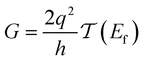
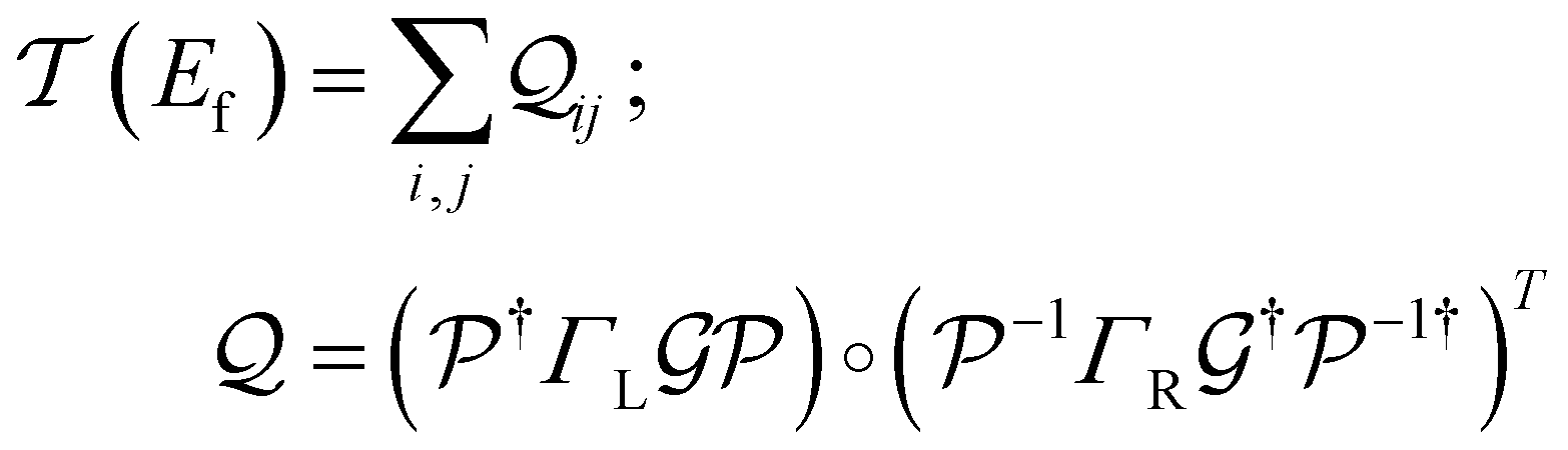
 are the eigenvectors of H′, termed conducting molecular orbitals (CMOs).42 The diagonal elements
  represent transmission contributions from the ith CMO and are always real and positive
  . The complex off-diagonal elements
  represent the quantum interference between CMOs i and j. The total quantum interference
  between ith and jth CMOs is always real as
  and when non-zero its sign indicates either constructive
  or destructive
  interference. Here, we define multi-orbital quantum interference between n CMOs as constructive (CQI) when
  and destructive (DQI) when
  . The manifestation of multi-orbital QIE for a simpler system i.e., benzene can be demonstrated through
  -factor analysis (see ESI,† Section S6) and we apply it here to analyze conductance boosts/suppressions across the TPx breadboards (Results subsections 2.2–2.3).
 where deff is an effective screening length and β = 30 nm−1. Here, we develop a more general molecule–electrode interaction model which accounts for the REA of any pair of atoms across the three breadboards. Specifically, while the peripheral ring meta/para N-atoms are fully electrode accessible, the peripheral ortho N-atoms and core N-atoms have reduced accessibilities which depend on the molecular conformation (Fig. 6D). A lower accessibility of the breadboard N-atoms sterically constrains the Au–N coordination to larger-than-optimal bond length. Below, we estimate the Au–N bond extension beyond the optimal coordination for all N-atoms across the three breadboards.
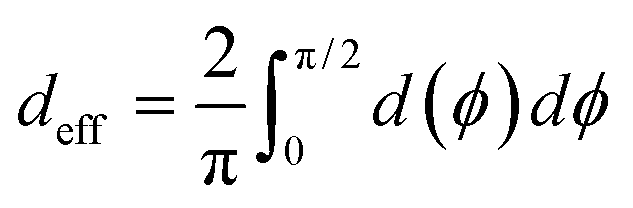
 —corresponding to two extreme Au–N coordination geometries with the electrode plane parallel and orthogonal to the pyridyl ring plane respectively, as lower and upper bounds for the screening distance. Effective Au–N electronic couplings given by eqn (7) were then estimated using α = exp(−βdeff) and with β = 30 nm−1 as the vacuum decay constant.69 Using eqn (10) we find αp = 1 and αc = 8.6 × 10⁻³ for TPm leading to a relative attenuation ratio
 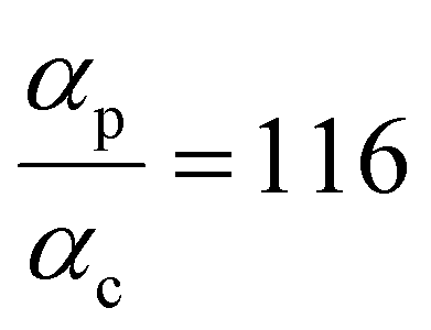 in agreement with our previous estimates in ref. 24. This model predicts slightly lower attenuation ratios
 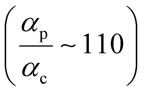 for TPp and significantly lower ratios
 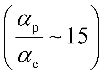 for TPo breadboards relative to that in TPm. The REA estimation procedure developed here is transferrable to other systems as highlighted by its application to OPE molecules (ESI,† Section S8) which are widely used in the study of single molecule junctions.
 and
and  for core N-atoms in TPm/o/p, whereas only the ortho-placed peripheral N-atom (TPo) is screened with
 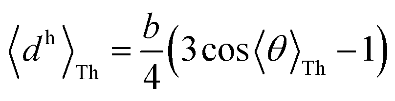 and
and  . Here, θ is the torsion angle between the peripheral and core rings.
b Attenuation factors computed with
. Here, θ is the torsion angle between the peripheral and core rings.
b Attenuation factors computed with  . Here, the brackets 〈〉Th represent a thermal average in which the contribution of each conformation is multiplied by its Boltzmann weight. The brackets 〈〉ϕ represent an averaging over the tilt angle ϕ as given by eqn (10).
c Attenuation factors computed with d = 〈d(ϕ = 0)〉Th.
d Attenuation factors computed with
. Here, the brackets 〈〉Th represent a thermal average in which the contribution of each conformation is multiplied by its Boltzmann weight. The brackets 〈〉ϕ represent an averaging over the tilt angle ϕ as given by eqn (10).
c Attenuation factors computed with d = 〈d(ϕ = 0)〉Th.
d Attenuation factors computed with  .
.
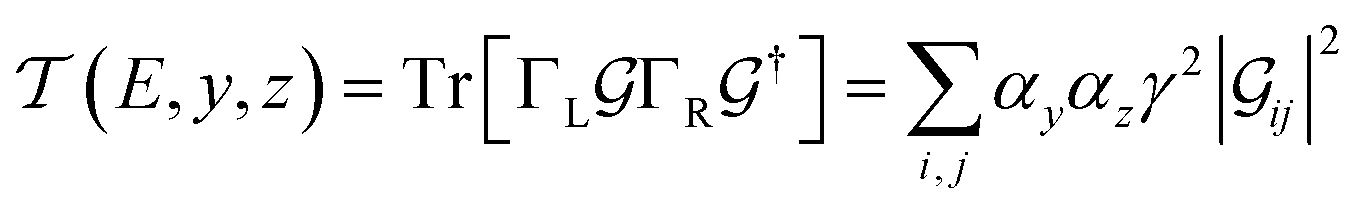
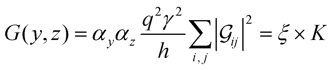
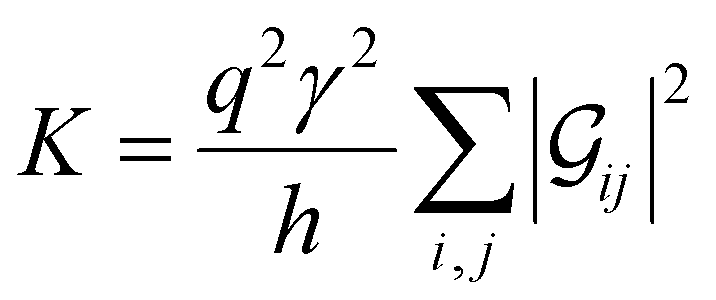 is a function of molecular conformation, and ξ = αyαz is a function of both molecule–electrode contacts and molecular conformation. Thus, we have: