
Interlayer engineering via alkaline hypophosphates for efficient and air-stable perovskite solar cells†
Jin
Peng
a,
Qiaofeng
Wu
a,
Hongming
Hou
a,
Taotao
Hu
a,
Yue
Huang
a,
Xudong
Cai
a,
Wenjie
Luo
a,
Xin
Chen
 b and
Hua
Yu
*a
b and
Hua
Yu
*a
aSchool of New Energy and Materials, Southwest Petroleum University, Chengdu 610500, P. R. China. E-mail: 201899010017@swpu.edu.cn; 17198328@qq.com
bCenter for Computational Chemistry and Molecular Simulation, College of Chemistry and Chemical Engineering, Southwest Petroleum University, Chengdu, 610500, China
First published on 15th March 2023
Abstract
The energy level mismatch and unfavorable interfacial reaction between nickel oxide (NiOx) and organic cations of the perovskite are the main factors affecting the power conversion efficiency (PCE) of inverted perovskite solar cells. Herein, interlayer engineering via dual-functional alkaline hypophosphite is introduced between the nickel oxide hole transport layer (HTL) and the perovskite layer. The introduction of alkaline hypophosphite deepens the valence band maximum of NiOx, which better aligns the energy band of perovskite solar cells with the best energy level matching using sodium hypophosphite. In addition, the deposition of alkaline sodium hypophosphite on NiOx reduces the proportion of Ni3+ and slows down the accelerated degradation of the perovskite layer caused by the reaction of excess Ni3+ with organic cations in the perovskite. The open-circuit voltage (VOC) of devices treated with sodium hypophosphite increased from 1.01 to 1.08 eV with a power conversion efficiency of 19.92%. Moreover, the unencapsulated devices retained 80% efficiency for 1000 hours under ambient conditions (50–60% relative humidity), and demonstrate a feasible and effective strategy for the fabrication of efficient and air-stable inverted perovskite solar cells.
Introduction
Organic–inorganic halide perovskite solar cells (PSCs) have garnered increasing attention over the past decade due to their commercial potential and dramatic increase in power conversion efficiency (PCE) from an initial 3.8% to 25.7%.1,2 PSCs have unique semiconducting properties that enable the fabrication of photovoltaic devices with normal (n–i–p) or inverted (p–i–n) configurations.3 Among these, inverted PSCs have attracted much attention due to their simple fabrication process, negligible hysteresis, low cost and excellent compatibility with tandem photovoltaics.4 However, the individual optoelectronic properties of inverted PSCs need to be further improved, especially the open-circuit voltage (VOC) and the short-circuit current density (JSC). In addition, factors such as moisture and oxygen in the environment can lead to the degradation of device performance. Meanwhile, in inverted PSCs, interface degradation is more severe and leads to nonradiative recombination losses at the carrier transport layer/perovskite interface. Therefore, improving the efficiency and stability of inverted PSCs is still an important issue for the commercial roadmap.5,6Selecting an inorganic material as a hole transport layer (HTL) is a good way to improve the optoelectronic properties and long-term stability of inverted PSCs. Compared with traditional organic hole transport materials, inorganic hole transport materials have more stable chemical stability and better hole mobility, and the cost is relatively lower.7 Nickel oxide (NiOx) is widely used as a hole transport layer in inverted perovskite solar cells.8,9 It has the advantages of a low band gap, high transmittance, and wide valence band edge.10–12 However, the interface defects between NiOx and the perovskite layer, mismatched energy level arrangement and charge distribution affect its performance and device stability is also affected by ion migration and the resulting chemical reaction and degradation.13 To date, a great deal of research has been done to address these issues, especially regarding interface modification. Cheng et al. modified NiOx with dipole molecule n-butylamine, and the density of defect states for the modified film decreased significantly.14 Chen et al. made NiOx with F6TCNNQ, which could reduce the shift level between perovskite and NiOx, which inhibits the voltage loss.15 Zhang et al. presented a self-assembled small-molecule to anchor NiOx and perovskite crystals, achieving dual passivation and suppressing adverse reactions at the NiOx–perovskite interface.16 Zhang et al. investigated the effect of CsBr modified layers on interfacial stress. The optimized interfacial hole extraction capability was significantly improved and the device obtained the highest efficiency of 19.7%.17 According to our research, the majority of research studies to date have used organic small molecules and materials that were self-synthesized to modify the surface of NiOx. This makes the process more difficult and expensive, which is not advantageous for commercialization. As a result, we have chosen a simple and cost-effective way to prepare perovskite solar cells.
In this work, we explored the effect of alkaline hypophosphates (NaH2PO2 and KH2PO2) by interfacial passivation of the NiOx layer on the performance of inverted PSCs. The introduction of hypophosphite can deepen the valence band maximum of the NiOx film, achieving the optimal energy level matching of NiOx and the perovskite layer. Besides, the degradation of the perovskite due to the reaction of Ni3+ with perovskite cations (MA+ and FA+) is slowed down, and the stability of the device is enhanced. Secondly, the introduction of an intermediate layer passivated the surface defects making a substantial increase in VOC. Ultimately, a champion PCE of 19.92% along with a VOC of 1.08 V, a JSC of 22.98 mA cm−2, and an FF of 80.13% is achieved. In addition, the unencapsulated devices retain more than 80% of their initial PCE value after 1000 hours of storage in ambient air at 50-60% relative humidity (RH).
Results and discussion
In this study, a MH2PO2 (MH2PO2, where M denotes Na or K) passivation layer was introduced between NiOx and the perovskite absorption layer using a post-treatment strategy. The structure of the device and its ideal molecular structure formula are shown in Fig. 1(a), and it is not obtained from atomistic simulations like DFT. Firstly, the effect of the MH2PO2 layer on the band structure is studied. The ultraviolet photoelectron spectra (UPS) of different NiOx films are shown in Fig. 1(b). The WFs (work functions) of NaH2PO2 and KH2PO2 modified NiOx were measured to be 4.28 eV and 4.27 eV, slightly up shifted about 0.06 eV and 0.05 eV compared with that of pristine NiOx (4.34 eV). The VBM values of NaH2PO2 and KH2PO2 modified NiOx were 1.12 eV and 1.08 eV, down shifted to 0.12 eV and 0.08 eV compared with that of pristine NiOx (1.00 eV). Therefore, after modification by NaH2PO2 and KH2PO2, the HOMO levels of the pristine NiOx (5.34 eV) were shifted to 5.40 eV and 5.35 eV.18Fig. 1(c)) shows the energy diagram of the device. After NaH2PO2 modification, the HOMO level of the HTL is closer to the VBM of the perovskite (5.4 eV), which minimizes the energy level mismatch at the HTL/perovskite interface and increases Voc.19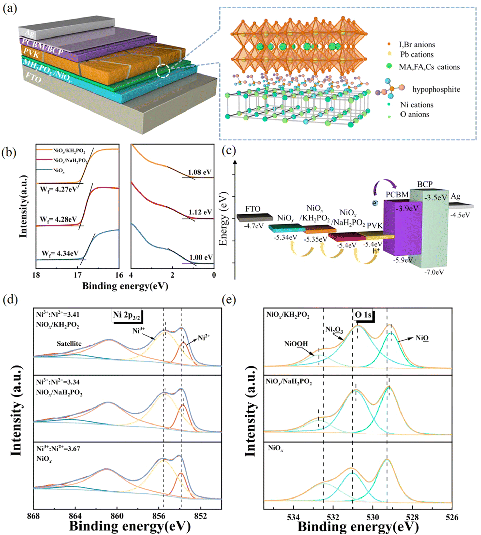 | ||
| Fig. 1 (a) Schematic diagram of the device structure and ideal molecular arrangement structure (not obtained from atomistic simulations). (b) UPS of NiOx and NiOx/MH2PO2. (c) Energy level diagram of the perovskite solar cells (PSCs) (data for the corresponding NiOx films are provided by the UPS measurement). High resolution XPS spectra of (d) Ni and (e) O elements in NiOx with and without MH2PO2 modification. | ||
Kelvin probe force microscopy (KPFM) was performed to further investigate the effect of MH2PO2 on the electronic energy levels of NiOx thin films. In Fig. 2a–c, the surface increased compared to the pristine NiOx film, indicating that the MH2PO2 treatment reduced the work function of NiOx. This is consistent with the UPS results. The surface morphology of NiOx under different treatments was investigated by the atomic force microscopy (AFM) measurement. Obviously, the MH2PO2 modification has a slight change in the surface morphology of the NiOx films, as shown in Fig. 2d–f. The X-ray photoemission spectrum (XPS) analysis is performed to explore the element composition of the NiOx films. Fig. 1(d) displays the XPS Ni 2p3/2 spectra. The ratios of Ni3+/Ni2+ calculated from the integral area in the Ni 2p spectrum are decreased from the pristine NiOx to the modified films. Previous studies have shown that the main reason for lower Voc is the occurrence of the redox reaction between metal cation sites (Ni3+ on the NiOx surface) and the A-site cation (MA+ or FA+), and this detrimental reaction generates a PbI2−rich hole extraction barrier at the NiOx–perovskite interface, which hinders its intrinsic conductivity and increases charge recombination, resulting in severe VOC loss.20,21 The reaction between the perovskite and NiOx is shown in the following reaction, where HA+ is a protonated A-site cation (CH5N2+or FA+, CH3NH3+ or MA+) and A is the deprotonated A-site cation (CH4N2, CH3NH2).
 | (1) |
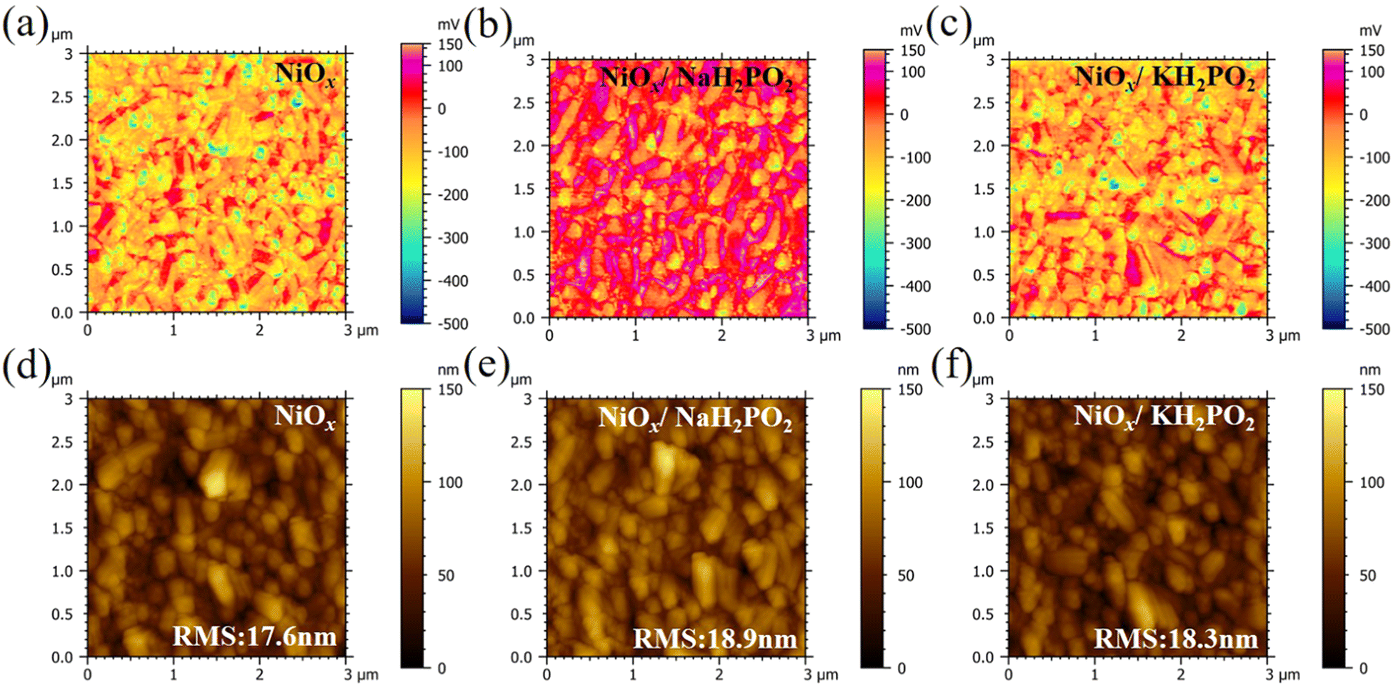 | ||
| Fig. 2 Surface potentials of the (a) pristine NiOx, (b) NaH2PO2 modified NiOx substrate, and (c) KH2PO2 modified NiOx substrate. AFM images of the (d) NiOx, (e) NaH2PO2 modified NiOx thin film, and (f) KH2PO2 modified NiOx thin film. | ||
Furthermore, it accelerates the degradation of the perovskite by deprotonation of the precursor amine and oxidation of iodide to interstitial iodine, resulting in severe device instability.22 Thus, the modified NiOx effectively suppresses the generation of crystal defects and the degradation of the perovskite layer, which is the main reason for the improved device stability. In addition, a shift of the Ni 2p3/2 peak to a lower binding energy is observed, indicating a charge transfer between NiOx and H2PO2−.23–25 The O 1s spectrum in Fig. 1(e) also has a shift in the peak position and a significant increase in the peak intensity, which leads to a change in the surface dipole and thus a shift in the vacuum energy level at the interface, facilitating hole injection into the hole transport layer.26 Besides, the peak of P 2p can be clearly observed in the NiOx-MH2PO2 modified film (Fig. S1a, ESI†), while the peak of the P element does not appear in the pristine NiOx, which can prove the existence of the H2PO2− molecule in the NiOx-MH2PO2 modified film. And the Na and K peaks in the modified film compared to the pristine thin film are shown in Fig. S1b and c (ESI†).
Fig. 3(a–c) shows the scanning electron microscopy (SEM) images of perovskite films. A slight increase in the average crystal size after modification was found compared to the pristine film, which was calculated using the Nano Measurer software (Fig. 3d). It is evident from the grain size distribution map of the perovskite films that the average grain size of the NiOx films modified by KH2PO2 increases the most, from 306 nm to 408 nm compared to the pristine films. Meanwhile, the cross-sectional SEM of the device is shown in Fig. S2 (ESI†). Fig. 3(e) shows the X-ray diffraction (XRD) patterns of the pristine and MH2PO2-modified perovskite films. It can be seen from the figure that the main peaks of the perovskite film are mainly located in 13.90°,19.80°, 24.31°, 28.20°, and 31.65°, which belong to the (001), (011), (111), (002), and (012) crystal planes of the cubic perovskite. The full-width half-maximum (FWHM) of modified crystal planes is narrower compared to the control device, as shown in Fig. 3(f), indicating an increase in grain size, the change of grain diameter is consistent with SEM. The ratio of peak intensities is calculated to further explore the effect on crystal orientation, (002)/(001) for different films. It was found that the (002)/(001) peak intensity ratio gradually increased after MH2PO2 modification, and the highest value of this ratio was observed in the NaH2PO2-modified devices, which exhibited the meritocratic orientation of the (001) crystal face. Moreover, the selective orientation on the (001) crystal plane facilitates the carrier transport at the interface.27–29 The UV-vis transmittance of the modified film was studied as shown in Fig. S3a (ESI†). The transmittance of the modified NiOx film in the visible light range is basically the same as that of the pristine film. Therefore, the introduction of the modification layer does not affect the performance of the device by reducing the transmittance of the film. Fig. 4(a) shows the UV-vis absorption spectrum of the perovskite film with increased light absorption in the wavelength range of 300 to 500 nm. This is due to the increase in light scattering caused by the increase in surface roughness, so the UV-vis spectra show an increase in light absorption, which contributes to the improvement of JSC.30 Fig. S3b (ESI†) shows that the surface hydrophilicity of the modified NiOx film decreases from 17.53° to 10.59°(NaH2PO2) and 9.77°(KH2PO2). This is favorable for subsequent perovskite deposition.31 Firstly, the effect of modification on the film quality is studied from the perspective of crystallography.
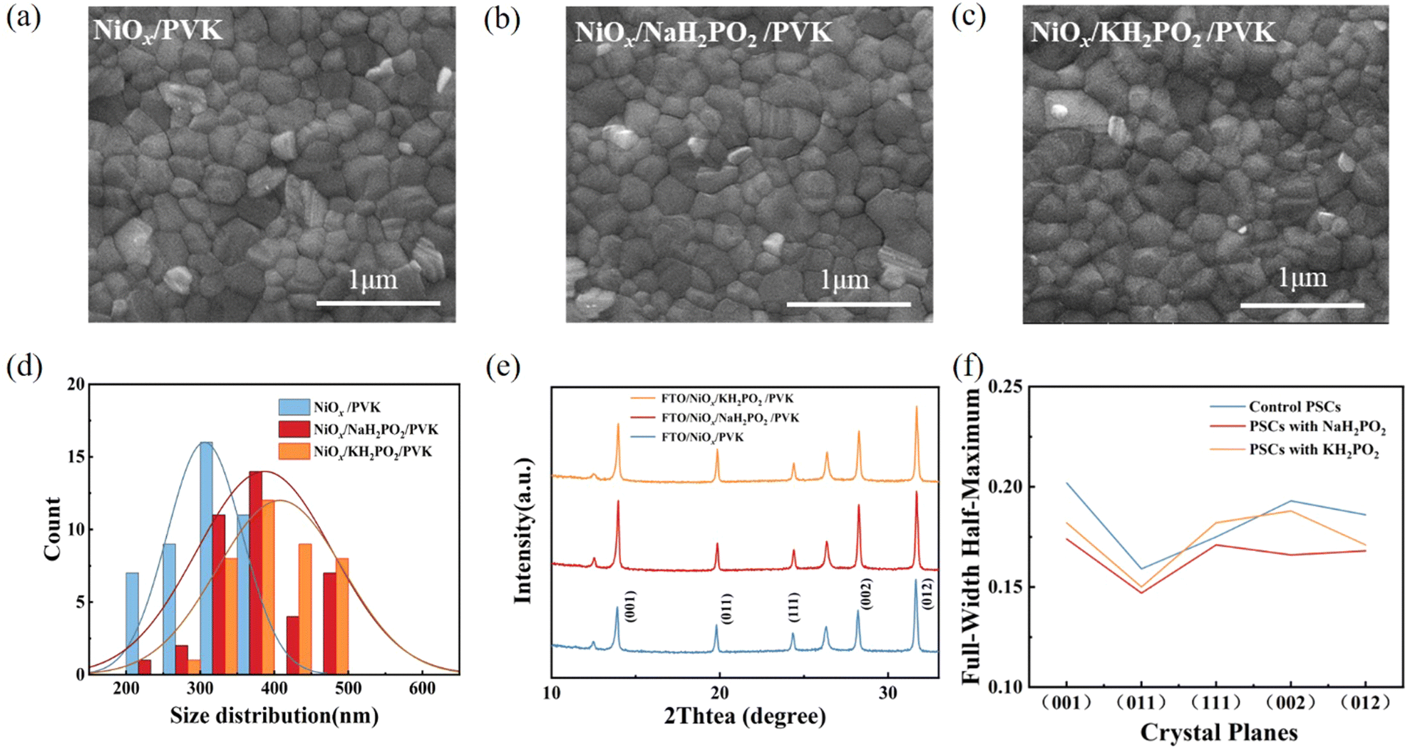 | ||
| Fig. 3 SEM images of the perovskite films on the (a) pristine NiOx, (b) NaH2PO2 modified NiOx substrate and (c) KH2PO2 modified NiOx substrate. (d) Histograms of the grain size (scale of data: 43 devices). (e) X-ray diffraction patterns of FTO/NiOx/PVK, FTO/NiOx/NaH2PO2/PVK and FTO/NiOx/KH2PO2/PVK. (f) Full-width half-maximum of XRD peaks for perovskite films with different devices. | ||
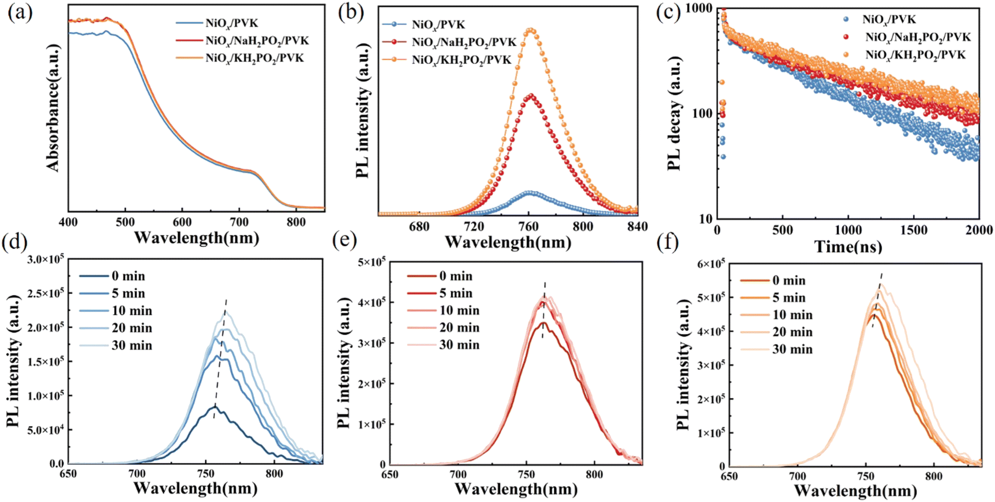 | ||
| Fig. 4 (a) UV-vis absorption spectra of the NiOx films with and without MH2PO2. (b) Steady PL spectra and (c) TRPL spectra of FTO/NiOx/PVK, FTO/NiOx/NaH2PO2/PVK and FTO/NiOx/KH2PO2/PVK. (d–f) PL spectra of perovskite films deposited on NiOx, NiOx/NaH2PO2 and NiOx/KH2PO2 under standard AM 1.5 irradiation (100 mW cm−2) for different times. | ||
To further elucidate the interfacial modification effect of alkali hypophosphite, steady-state photoluminescence (PL) and time-resolved photoluminescence (TRPL) measurements were performed, respectively (Fig. 4(b) and (c)), and the obtained results are shown in Table S1 (ESI†). The samples modified with NaH2PO2 and KH2PO2 exhibit stronger luminescence intensity compared to that of the modified films, which is the same as the previous study on the interfacial modification of alkali metal salts, indicating the suppression of non-radiative recombination.32,33 Secondly, the luminescence intensity of KH2PO2 is higher than that of NaH2PO2, and that of the modified devices is significantly greater than that of the original devices. This suggests effective quasi-Fermi-level splitting, which may be the reason for the increased VOC. However, the TRPL test results show an extended decay lifetime, which implies a slower carrier extraction rate. The lifetime of KH2PO2 (984.79) modified is longer than that of NaH2PO2 (863.07), and the lifetimes of both are higher than that of the pristine film (660.81), which implies a slower carrier extraction rate. This seems to be contrary to our idea of interfacial modification of NiOx, so we can infer that MH2PO2 has a dual role here. On the one hand, MH2PO2 can reduce non-radiative surface recombination, passivate surface defects, and prevent NiOx from reacting unfavorably with the perovskite film. On the other hand, the longer decay lifetime of perovskite films formed on the NiOx-MH2PO2 substrates shows a slower rate of recombination, which is attributed to the passivation of grain boundaries by alkali metal ions. Also, because the enhanced steady-state luminescence intensity also mitigates the nonradiative recombination, with longer carrier lifetimes allowing an increase in JSC. However, because the carrier lifetime of KH2PO2 is increased by about one-third compared to the pristine device, the hole extraction rate is too slow, which affects its VOC, and the defect state density of NaH2PO2 is smaller compared to that of KH2PO2. Maybe this is the reason why the VOC of KH2PO2 is not as good as that of NaH2PO2. It has been reported that alkali metal cations can suppress ion migration.34,35 Therefore, we placed the pristine films and the modified films under continuous irradiation of light to observe the change in the PL intensity. With the increasing illumination time, a clear increase in fluorescence intensity and a red shift of the PL peak can be observed in the pristine film (Fig. 4(d)), indicating an increase in interfacial defects and aggravation of interfacial reactions,16 while the NaH2PO2-modified films show a relatively little change (Fig. 4(e)). The reason for the increase in luminescence intensity with illumination time in perovskite films is due to Ii defects and iodide migration.36 Therefore, NaH2PO2 has a certain effect on reducing nonradiative recombination, suppress ion migration, and accelerate the transport of photocarriers; thus, devices with better optoelectronic properties can be obtained. This may be one reason why the NaH2PO2-modified device performs better.
To further investigate the interfacial traps and recombination, Fig. 5(a) displays the extended C–V curves that directly compare the built-in potential of the devices by the Mott–Schottky analysis using the following equation37
 | (2) |
VOC = nKT![[thin space (1/6-em)]](https://www.rsc.org/images/entities/char_2009.gif) ln(I)/q + C ln(I)/q + C | (3) |
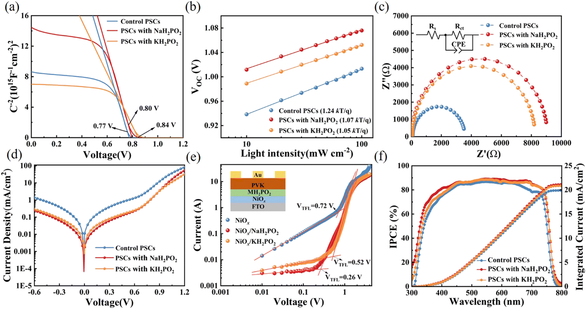 | ||
| Fig. 5 (a) Mott–Schottky plot of capacitance–voltage measurements of devices based on different HTLs. (b) VOC as a function of light intensity. (c) EIS of PSCs in the dark; the inset shows the equivalent circuit. (d) Dark J–V curves of devices with different NiOx-based HTLs. (e) Dark J–V curves with the SCLC model based on the device structure of FTO/NiOx/Au or MH2PO2-modified NiOx/PVK/Au. (f) IPCE spectrum together with the integrated JSC of the PSCs. | ||
Corresponding values of series resistance (Rs) and charge transfer resistance (Rct) are summarized in Table S2 (ESI†). The larger semicircle of devices compares pristine (3476 Ω) to those modified with NaH2PO2 (9033 Ω) and KH2PO2 (8187 Ω) shows the enhanced Rct, indicating that charge recombination at the perovskite/HTL is suppressed.23 Furthermore, the dark-current curves versus bias voltage (−0.6 to 1.2 V) of the pristine and modified devices shown in Fig. 5(d), which also verifies the reduction of trap content. Compared with the pristine NiOx and KH2PO2 in the work bias region, the leakage current of the NaH2PO2 modified device is smaller, which is beneficial to the improvement of JSC.41 Space-charge-limited-current (SCLC) is used to measure the hole transport process to estimate the internal trap density of the device. The hole-only device was constructed with FTO/NiOx/PVK/Au and FTO/MH2PO2-modified NiOx/PVK/Au structures (Fig. 5(e)). It is found that the NaH2PO2-modified device exhibits a lower density of defect states (6.06 × 1012 cm−3) compared to those of the pristine device (1.68 × 1013 cm−3) and KH2PO2-based device (1.21 × 1013 cm−3), which is consistent with the previous test results. This shows that NaH2PO2 can reduce the defect density between NiOx and the perovskite layer and improve the VOC of the device.42,43 Overall, the application of MH2PO2-modified NiOx can facilitate charge transport at the perovskite/HTL and reduce carrier recombination, mainly due to improved electrical conductivity, optimized interfacial energy alignment, and suppressed interfacial defects, thereby significantly improving the photovoltaic performance of the device.
We have demonstrated the beneficial effect of an alkali metal hypophosphite passivation strategy to improve PSC performance. The FTO/NiOx/MH2PO2/(CsPbI3)0.05[(FAPbI3)0.85(MAPbBr3)0.15]0.95/PC61BM/BCP/Ag structure was used to further study the photovoltaic performance of PSCs. After experiments, NaH2PO2 and KH2PO2 exhibited the best PCE in the device at a concentration of 4 mg mL−1 (Fig. S4, ESI†). And in Fig. 6(a) and Table 1 we can observe an obvious improvement of photovoltaic performance, as well as stabilized JSC and efficiency. Fig. 6(b) compares the J–V curves of the best device based on pristine NiOx and modified films with MH2PO2. Furthermore, there is an excellent agreement between the short-circuit current density values from the experiments and those estimated from the measured external quantum efficiency (EQE) spectra in Fig. 5(f). Clearly, the fill factor (FF) difference between devices under different conditions is negligible. The improvement of VOC and JSC is the main factor to improve the efficiency of the device. The pristine device exhibited a PCE of 17.86%, with a VOC of 1.02 V, a JSC of 21.87 mA cm−2, and an FF of 79.73%. However, the NaH2PO2-modified NiOx-based device shows the best performance with a maximum PCE of 19.92%, a VOC of 1.08 V, a JSC of 22.98 mA cm−2, and an FF of 80.13%.
 | ||
| Fig. 6 (a) Photovoltaic parameter statistics for the investigated PSCs extracted by the J–V characteristics. (b) Stabilized J–V curves of the best-performing devices with different modification layers compared with control devices. (c) Long-term normalized stability of PSCs with pristine NiOx and MH2PO2 modified NiOx HTLs (under ambient air with a relative humidity of 50–60%). (d) Normalized averaged PCE of the corresponding devices kept under a N2 atmosphere at 60 °C for 1000 h. (e) Operational stability tests by tracking their MPP under 1-sun equivalent white LED illumination. Values are normalized to the initial PCE at MPP. | ||
| Devices | Sweep | V OC (V) | J SC (mA cm−2) | FF | PCE (%) |
|---|---|---|---|---|---|
| NiOx | FS | 1.01 | 21.82 | 79.58 | 17.62 |
| RS | 1.01 | 21.79 | 79.91 | 17.60 | |
| NiOx/NaH2PO2 | FS | 1.08 | 22.93 | 77.04 | 19.10 |
| RS | 1.08 | 22.98 | 80.13 | 19.92 | |
| NiOx/KH2PO2 | FS | 1.06 | 22.16 | 79.86 | 18.78 |
| RS | 1.06 | 22.16 | 80.62 | 18.91 |
The long-term stability of devices is also an important factor restricting commercial development. Therefore, the long-term stability of the pristine and modified devices after 1000 h storage in ambient air at 50-60% relative humidity was investigated. As shown in Fig. 6(c), the performance of the pristine device dropped below 60% after 1000 hours, while that of the MH2PO2-modified device retained around 80% of the initial efficiency during the same period. It was confirmed that the introduction of the MH2PO2 modification layer is beneficial to improve the air stability of the device, as the MH2PO2 buffer layer can improve the perovskite/HTL interfacial contact and perovskite crystallinity, thereby mitigating water intrusion or penetration.17,44 In addition, the PCE of the NaH2PO2-based device can remain above 80% of the initial value after 1000 h storage at 60 °C under a nitrogen atmosphere (Fig. 6(d)), while the performance of the pristine device is severely degraded. The operational stability of the unencapsulated pristine device and the MH2PO2 modified devices are also tested under continuous 1 sun illumination (achieved by a white-light LED array) with MPP tracking in ambient air as shown in Fig. 6(e).45–47 The MH2PO2 modified device maintained around 90% of its initial PCE after 6000 min, much higher than that of the pristine device (70%). The effective defect passivation on the perovskite surface and the enhancement of perovskite crystallinity makes the stability of MH2PO2 modified devices significantly enhanced under different conditions. These test results confirm the impressive role of MH2PO2 in improving the long-term stability of the devices.
Conclusions
Through interface engineering, the NiOx interface defects are passivated via alkaline hypophosphates. The energy level can be altered to improve the hole transport efficiency by adding NaH2PO2 to modify NiOx. Additionally, by preventing the damaging redox processes at the NiOx/perovskite interface, the degradation of the perovskite layer is slowed down, increasing the device's stability. Furthermore, the devices changed by NaH2PO2 have a lower trap-state density, which improves VOC. Therefore, the NiOx/NaH2PO2-based PSCs show champion PCE values with a negligible hysteresis increase from 17.60% to 19.92%, a VOC increase from 1.01 V to 1.08 V, and a JSC increase from 21.79 mA cm−2 to 22.98 mA cm−2. Meanwhile, the NaH2PO2-modified device also exhibits excellent long-term stability, maintaining 80% of the initial efficiency after being stored in air at 50-60% RH for 1000 h. This simple and economical passivation strategy provides a new approach for preparing efficient and stable PSCs as well as commercializing them for applications.Experimental
Materials
Methyl-ammonium bromine (MABr, ≥99.5%), lead(II) iodide (PbI2, >99.99%), formamidinium iodide (FAI, ≥99.5%), lead(II) bromine (PbBr2, >99.99%), 2,9-dimethyl-4,7-dipheny l-1,10-phenanthroline (BCP, >99%), and cesium iodide (CsI, >99.99%) were manufactured from Xi’an Polymer Light Technology Corp. Ethanol (ET, 99.5%), isopropanol (IPA, 99.8%), sodium hypophosphite monohydrate (NaH2PO2·H2O, 99%), ethanolamine (ETA, 99%), and potassium hypophosphite (KH2PO2, 99%) were brought from Aladdin. Chlorobenzene (CB, 99.8%), N,N-dimethylformamide (DMF, 99.8%), ethyl acetate (EA, 99.8%), and dimethyl sulfoxide (DMSO, 99.9%) were purchased from Sigma-Aldrich. [6,6]Phenyl C-61-butyric acid methyl ester (PC61BM, 99.5%) and nickel(II) acetate tetrahydrate (Ni–(CH3COOH)2·4H2O, 99%) were manufactured by Organtec Ltd and Acros Organics, respectively. All chemicals and solvents were used directly as received.Device fabrication
The device was made using an FTO glass substrate that measures 1.6 × 2 cm2. Detergent, ethanol, acetone, and ethanol are all used to wash the FTO glass for 15 minutes. The substrates are then moved into a UV-ozone oven for 10 minutes. NiOx precursor solutions are made according to earlier publications.48 The NiOx precursor solution was created by dissolving Ni–(CH3COOH)2·4H2O (25 mg mL−1) in ethanol, adding 6 μL of ETA additive per mL, and agitating the mixture for 8 hours at 60 °C. After this, the NiOx solution was produced, deposited onto the FTO substrate for 40 s at 1500 rpm, and then annealed for 60 min in an atmosphere of air at 300 °C. The corresponding powders were added to deionized water and stirred for 2 hours to obtain MH2PO2 solutions of different concentrations. The MH2PO2 solution was deposited on the NiOx layer by spin-coating at 1500 rpm. for 30 s and annealed at 150 °C for 10 min. The perovskite precursor solution (FAI:MABr:CsI:PbI2:PbBr2 = 199.8 mg:26.7 mg:18.2 mg:573.9 mg:87.4 mg dissolved in 1 mL of DMF:DMSO = 4:1 (v/v), and stirred at 60 °C for 1 h) was spin coated on pure or modified NiOx at 3000 rpm for 35 s. After 27 s of spin-coating, 200 L of ethyl acetate was swiftly dropped over the substrates. Then, 20 mg mL−1 PC61BM was dissolved in chlorobenzene and fabricated on the perovskite film at 1500 rpm for 40 s and annealed at 80 °C for 10 min. Then, the coating was spun at 4000 rpm for 30 s for 0.5 mg mL−1, 30 s in isopropanol solution. Finally, heat evaporation was used to deposit a 100 nm thick Ag electrode on the film surface.
Characterization
Ultraviolet photoelectron spectroscopy (UPS) was performed using a PHI 5000 VersaProbe III with He I source (21.22 eV) under an applied negative bias of 9.0 V. The external quantum efficiency (EQE) was performed using a Bentham PVE300 Photovoltaic Device Characterization System from 300 nm to 800 nm. The scanning electron microscopy (SEM) image films were observed using a scanning electron microscope (FEI INSPECT F50, U.S.A.). X-ray diffraction (XRD) measurements were performed using a X-ray diffractometer (PANalytical B.V., X’ Pert Pro MPD). A ESCALAB 250Xi instrument with a monochromatized Al Kα X-ray source in vacuum was used to perform XPS measurements. Illumination was provided using an AAA Class Simulator (SS-F5-3A, Enli Technology Co., Ltd) under an AM 1.5G spectrum and a light intensity of 100 mW cm−2. AFM and KPFM images (KEYSIGHT 7500 AFM/STM) were characterized to study the surface morphology and surface potentials. The PL and TRPL images were recorded using an Edinburgh FLS 980 spectrophotometer.Conflicts of interest
There are no conflicts to declare.Acknowledgements
This work was financially supported by the Sichuan Science and Technology Program (2021YFH0090) and the Chengdu Science and Technology Program (2021GH0200032HZ).Notes and references
- A. Kojima, K. Teshima, Y. Shirai and T. Miyasaka, Organometal Halide Perovskites as Visible-Light Sensitizers for Photovoltaic Cells, J. Am. Chem. Soc., 2009, 131, 6050–6051 CrossRef CAS PubMed.
- NREL, Best research-cell efficiencies chart, https://www.nrel.gov/pv/cell-efficiency.html.
- L. Meng, J. You, T. F. Guo and Y. Yang, Recent Advances in the Inverted Planar Structure of Perovskite Solar Cells, Acc. Chem. Res., 2016, 49, 155–165 CrossRef CAS PubMed.
- Y.-H. Seo, I. H. Cho and S.-I. Na, Investigation of sol-gel and nanoparticle-based NiOx hole transporting layer for high-performance planar perovskite solar cells, J. Alloys Compd., 2019, 797, 1018–1024 CrossRef CAS.
- M. L. Agiorgousis, Y. Y. Sun, H. Zeng and S. Zhang, Strong covalency-induced recombination centers in perovskite solar cell material CH3NH3PbI3, J. Am. Chem. Soc., 2014, 136, 14570–14575 CrossRef CAS PubMed.
- G. Niu, X. Guo and L. Wang, Review of recent progress in chemical stability of perovskite solar cells, J. Mater. Chem. A, 2015, 3, 8970–8980 RSC.
- D. Hou, J. Zhang, X. Gan, H. Yuan, L. Yu, C. Lu, H. Sun, Z. Hu and Y. Zhu, Pb and Li co-doped NiOx for efficient inverted planar perovskite solar cells, J. Colloid Interface Sci., 2020, 559, 29–38 CrossRef CAS PubMed.
- L. Xu, X. Chen, J. Jin, W. Liu, B. Dong, X. Bai, H. Song and P. Reiss, Inverted perovskite solar cells employing doped NiO hole transport layers: A review, Nano Energy, 2019, 63, 103860 CrossRef CAS.
- X. Yin, Y. Guo, H. Xie, W. Que and L. B. Kong, Nickel Oxide as Efficient Hole Transport Materials for Perovskite Solar Cells, Sol. RRL, 2019, 3, 1900001 CrossRef.
- A. Fakharuddin, M. Vasilopoulou, A. Soultati, M. I. Haider, J. Briscoe, V. Fotopoulos, D. Di Girolamo, D. Davazoglou, A. Chroneos, A. R. B. M. Yusoff, A. Abate, L. Schmidt-Mende and M. K. Nazeeruddin, Robust Inorganic Hole Transport Materials for Organic and Perovskite Solar Cells: Insights into Materials Electronic Properties and Device Performance, Sol. RRL, 2020, 5, 2000555 CrossRef.
- R. Singh, P. K. Singh, B. Bhattacharya and H.-W. Rhee, Review of current progress in inorganic hole-transport materials for perovskite solar cells, Appl. Mater. Today, 2019, 14, 175–200 CrossRef.
- S. Madani, T. Tesfamichael, H. Wang and N. Motta, Study of Pb-based and Pb-free perovskite solar cells using Cu-doped Ni1-xO thin films as hole transport material, Ceram. Int., 2022, 48, 15207–15217 CrossRef CAS.
- W. Chen, Y. Zhou, G. Chen, Y. Wu, B. Tu, F. Z. Liu, L. Huang, A. M. C. Ng, A. B. Djurišić and Z. He, Alkali Chlorides for the Suppression of the Interfacial Recombination in Inverted Planar Perovskite Solar Cells, Adv. Energy Mater., 2019, 9, 1803872 CrossRef.
- Y. Cheng, M. Li, X. Liu, S. H. Cheung, H. T. Chandran, H.-W. Li, X. Xu, Y.-M. Xie, S. K. So, H.-L. Yip and S.-W. Tsang, Impact of surface dipole in NiOx on the crystallization and photovoltaic performance of organometal halide perovskite solar cells, Nano Energy, 2019, 61, 496–504 CrossRef CAS.
- W. Chen, Y. Zhou, L. Wang, Y. Wu, B. Tu, B. Yu, F. Liu, H. W. Tam, G. Wang, A. B. Djurisic, L. Huang and Z. He, Molecule-Doped Nickel Oxide: Verified Charge Transfer and Planar Inverted Mixed Cation Perovskite Solar Cell, Adv. Mater., 2018, 30, e1800515 CrossRef PubMed.
- J. Zhang, J. Yang, R. Dai, W. Sheng, Y. Su, Y. Zhong, X. Li, L. Tan and Y. Chen, Elimination of Interfacial Lattice Mismatch and Detrimental Reaction by Self-Assembled Layer Dual-Passivation for Efficient and Stable Inverted Perovskite Solar Cells, Adv. Energy Mater., 2022, 12, 2103674 CrossRef CAS.
- B. Zhang, J. Su, X. Guo, L. Zhou, Z. Lin, L. Feng, J. Zhang, J. Chang and Y. Hao, NiO/Perovskite Heterojunction Contact Engineering for Highly Efficient and Stable Perovskite Solar Cells, Adv. Sci., 2020, 7, 1903044 CrossRef CAS PubMed.
- L. Xie, Z. Cao, J. Wang, A. Wang, S. Wang, Y. Cui, Y. Xiang, X. Niu, F. Hao and L. Ding, Improving energy level alignment by adenine for efficient and stable perovskite solar cells, Nano Energy, 2020, 74, 104846 CrossRef CAS.
- Q. Liu, Y. Jiang, K. Jin, J. Qin, J. Xu, W. Li, J. Xiong, J. Liu, Z. Xiao, K. Sun, S. Yang, X. Zhang and L. Ding, 18% Efficiency organic solar cells, Sci. Bull., 2020, 65, 272–275 CrossRef CAS PubMed.
- B. Traore, L. Pedesseau, J. C. Blancon, S. Tretiak, A. D. Mohite, J. Even, C. Katan and M. Kepenekian, Importance of Vacancies and Doping in the Hole-Transporting Nickel Oxide Interface with Halide Perovskites, ACS Appl. Mater. Interfaces, 2020, 12, 6633–6640 CrossRef CAS PubMed.
- C. C. Boyd, R. C. Shallcross, T. Moot, R. Kerner, L. Bertoluzzi, A. Onno, S. Kavadiya, C. Chosy, E. J. Wolf, J. Werner, J. A. Raiford, C. de Paula, A. F. Palmstrom, Z. J. Yu, J. J. Berry, S. F. Bent, Z. C. Holman, J. M. Luther, E. L. Ratcliff, N. R. Armstrong and M. D. McGehee, Overcoming Redox Reactions at Perovskite-Nickel Oxide Interfaces to Boost Voltages in Perovskite Solar Cells, Joule, 2020, 4, 1759–1775 CrossRef CAS.
- R. C. S. C. C. Boyd, T. Moot, R. Kerner, L. Bertoluzzi, A. Onno, S. Kavadiya, C. Chosy, E. J. Wolf, J. Werner, J. A. Raiford, A. F. P. C. de Paula, Z. J. Yu, J. J. Berry, S. F. Bent, Z. C. Holman, J. M. Luther, E. L. Ratcliff, N. R. Armstrong and M. D. McGehee, Overcoming Redox Reactions at PerovskiteNickel Oxide Interfaces to Boost Voltages in Perovskite Solar Cells, Joule, 2020, 4, 1759 CrossRef.
- D. Z. Xuefeng Xia, X. Wang, Z. Xiao and F. Li, A carbon-quantum-dot-hybridized NiOx hole-transport layer enables efficient and stable planar p–i–n perovskite solar cells with high open-circuit voltage, J. Mater. Chem. C, 2021, 9, 12213 RSC.
- Y. Hu, Z. Yang, X. Cui, P. Zeng, F. Li, X. Liu, G. Feng and M. Liu, Construction of Charge Transport Channels at the NiOx/Perovskite Interface through Moderate Dipoles toward Highly Efficient Inverted Solar Cells, ACS Appl. Mater. Interfaces, 2022, 14, 13431–13439 CrossRef CAS PubMed.
- X. Zhao, W. Zhang, X. Feng, X. Guo, C. Lu, X. Li and J. Fang, Photoconductive NiOx hole transport layer for efficient perovskite solar cells, Chem. Eng. J., 2022, 435, 135140 CrossRef CAS.
- S. Liu, R. Liu, Y. Chen, S. Ho, J. H. Kim and F. So, Nickel Oxide Hole Injection/Transport Layers for Efficient Solution-Processed Organic Light-Emitting Diodes, Chem. Mater., 2014, 26, 4528–4534 CrossRef CAS.
- G. Uzurano, N. Kuwahara, T. Saito, A. Fujii and M. Ozaki, Orientation Control of 2D Perovskite in 2D/3D Heterostructure by Templated Growth on 3D Perovskite, ACS Mater. Lett., 2022, 4, 378–384 CrossRef CAS.
- Z. Xu, Z. Liu, N. Li, G. Tang, G. Zheng, C. Zhu, Y. Chen, L. Wang, Y. Huang, L. Li, N. Zhou, J. Hong, Q. Chen and H. Zhou, A Thermodynamically Favored Crystal Orientation in Mixed Formamidinium/Methylammonium Perovskite for Efficient Solar Cells, Adv. Mater., 2019, 31, e1900390 CrossRef PubMed.
- G. Zheng, C. Zhu, J. Ma, X. Zhang, G. Tang, R. Li, Y. Chen, L. Li, J. Hu, J. Hong, Q. Chen, X. Gao and H. Zhou, Manipulation of facet orientation in hybrid perovskite polycrystalline films by cation cascade, Nat. Commun., 2018, 9, 2793 CrossRef PubMed.
- Q. Chen, C. Peng, L. Du, T. Hou, W. Yu, D. Chen, H. Shu, D. Huang, X. Zhou, J. Zhang, W. Zhang, H. Li, J. Xie and Y. Huang, Synergy of mesoporous SnO2 and RbF modification for high-efficiency and stable perovskite solar cells, J. Energy Chem., 2022, 66, 250–259 CrossRef CAS.
- M. Pylnev, A. M. Barbisan and T.-C. Wei, Effect of wettability of substrate on metal halide perovskite growth, Appl. Surf. Sci., 2021, 541, 148559 CrossRef CAS.
- S. Zhang, H. Wang, X. Duan, L. Rao, C. Gong, B. Fan, Z. Xing, X. Meng, B. Xie and X. Hu, Printable and Homogeneous NiOx Hole Transport Layers Prepared by a Polymer-Network Gel Method for Large-Area and Flexible Perovskite Solar Cells, Adv. Funct. Mater., 2021, 31, 2106495 CrossRef CAS.
- P. Zhu, S. Gu, X. Luo, Y. Gao, S. Li, J. Zhu and H. Tan, Simultaneous Contact and Grain-Boundary Passivation in Planar Perovskite Solar Cells Using SnO2-KCl Composite Electron Transport Layer, Adv. Energy Mater., 2019, 10, 1903083–1903090 CrossRef.
- M. Abdi-Jalebi, Z. Andaji-Garmaroudi, S. Cacovich, C. Stavrakas, B. Philippe, J. M. Richter, M. Alsari, E. P. Booker, E. M. Hutter, A. J. Pearson, S. Lilliu, T. J. Savenije, H. Rensmo, G. Divitini, C. Ducati, R. H. Friend and S. D. Stranks, Maximizing and stabilizing luminescence from halide perovskites with potassium passivation, Nature, 2018, 555, 497–501 CrossRef CAS PubMed.
- D. Y. Son, S. G. Kim, J. Y. Seo, S. H. Lee, H. Shin, D. Lee and N. G. Park, Universal Approach toward Hysteresis-Free Perovskite Solar Cell via Defect Engineering, J. Am. Chem. Soc., 2018, 140, 1358–1364 CrossRef CAS PubMed.
- D. W. deQuilettes, W. Zhang, V. M. Burlakov, D. J. Graham, T. Leijtens, A. Osherov, V. Bulovic, H. J. Snaith, D. S. Ginger and S. D. Stranks, Photo-induced halide redistribution in organic-inorganic perovskite films, Nat. Commun., 2016, 7, 11683 CrossRef CAS PubMed.
- J. Yang, S. Xiong, J. Song, H. Wu, Y. Zeng, L. Lu, K. Shen, T. Hao, Z. Ma, F. Liu, C. Duan, M. Fahlman and Q. Bao, Energetics and Energy Loss in 2D Ruddlesden–Popper Perovskite Solar Cells, Adv. Energy Mater., 2020, 10, 2000687 CrossRef CAS.
- G. Yang, C. Wang, H. Lei, X. Zheng, P. Qin, L. Xiong, X. Zhao, Y. Yan and G. Fang, Interface engineering in planar perovskite solar cells: energy level alignment, perovskite morphology control and high performance achievement, J. Mater. Chem. A, 2017, 5, 1658–1666 RSC.
- Q. Wu, T. Hu, C. Liu, Y. Yu, H. Hou, R. Liu, M. Zhang and H. Yu, Efficient Energy Level Modulation via Electrophilic KBF4 for High-Performance Inverted Planar Perovskite Solar Cells with Superior Stability, J. Phys. Chem. C, 2022, 126, 3375–3384 CrossRef CAS.
- H. Hou, T. Hu, F. Zhang, R. Liu, J. He, C. Liu, Y. Yu, D. Chen, Q. Wu, M. Zhang and H. Yu, Small molecule interfacial cross-linker for highly efficient two-dimensional perovskite solar cells, J. Energy Chem., 2022, 68, 35–41 CrossRef CAS.
- X. Chen, L. Xu, C. Chen, Y. Wu, W. Bi, Z. Song, X. Zhuang, S. Yang, S. Zhu and H. Song, Rare earth ions doped NiO hole transport layer for efficient and stable inverted perovskite solar cells, J. Power Sources, 2019, 444, 227267 CrossRef CAS.
- W. Liu, J. Xiong, N. Liu, J. Dai, Z. Dai, Y. Huang, Z. Zhang, X. Xue, Q. Dai and J. Zhang, Defect passivation and interface modification by tetra-n-octadecyl ammonium bromide for efficient and stable inverted perovskite solar cells, Chem. Eng. J., 2022, 429, 132426 CrossRef CAS.
- X. Deng, Z. Cao, C. Li, S. Wang and F. Hao, Benzotriazole derivative inhibits nonradiative recombination and improves the UV-stability of inverted MAPbI3 perovskite solar cells, J. Energy Chem., 2022, 65, 592–599 CrossRef CAS.
- H. C. Yang Bai, S. Xiao, Q. Xue, T. Zhang, Z. Zhu, Q. Li, C. Hu, Y. Yang, Z. Hu, F. Huang, K. Sing Wong, H.-L. Yip and S. Yang, Effects of a Molecular Monolayer Modifi cation of NiO Nanocrystal Layer Surfaces on Perovskite Crystallization and Interface Contact toward Faster Hole Extraction and Higher Photovoltaic Performance, Adv. Funct. Mater., 2016, 26, 2950 CrossRef.
- S. Fu, X. Li, L. Wan, Y. Wu, W. Zhang, Y. Wang, Q. Bao and J. Fang, Efficient Passivation with Lead Pyridine-2-Carboxylic for High-Performance and Stable Perovskite Solar Cells, Adv. Energy Mater., 2019, 9, 1901852 CrossRef.
- S. Liu, R. Chen, X. Tian, Z. Yang, J. Zhou, F. Ren, S. Zhang, Y. Zhang, M. Guo, Y. Shen, Z. Liu and W. Chen, Boost the efficiency of nickel oxide-based formamidinium-cesium perovskite solar cells to 21% by using coumarin 343 dye as defect passivator, Nano Energy, 2022, 94, 106935 CrossRef CAS.
- W. Zhang, X. Li, X. Feng, X. Zhao and J. Fang, A conjugated ligand interfacial modifier for enhancing efficiency and operational stability of planar perovskite solar cells, Chem. Eng. J., 2021, 412, 128680 CrossRef CAS.
- T. Hu, F. Zhang, H. Yu, M. Zhang, Y. Yu, W. Zhang, R. Liu, L. Tian and Z. Ma, Efficient carrier transport via dual-function interfacial engineering using cesium iodide for high-performance perovskite solar cells based on NiOx hole transporting materials, Nano Res., 2021, 14, 3864–3872 CrossRef CAS.
Footnote |
| † Electronic supplementary information (ESI) available. See DOI: https://doi.org/10.1039/d3qm00103b |
| This journal is © the Partner Organisations 2023 |