DOI:
10.1039/D3NJ01820B
(Paper)
New J. Chem., 2023,
47, 15162-15174
Solar energy harvesting by a PtS2/ZrS2 van der Waals heterostructure†
Received
20th April 2023
, Accepted 19th July 2023
First published on 20th July 2023
Abstract
In this study, the photovoltaic performance of van der Waals heterostructure (v-HS) PtS2/ZrS2 has been examined using density functional theory based on first-principle calculations. Out of six possible configurations of v-HS of PtS2/ZrS2, the most stable configuration of v-HS of PtS2/ZrS2 has been identified based on adhesion energy and phonon dispersion relation. The Heyd–Scuseria–Ernzerhof functional has been employed for the calculation of the electronic properties, which has shown that the v-HS PtS2/ZrS2 possesses a type II indirect band gap. The results based on the absorption coefficient have indicated that the v-HS of PtS2/ZrS2 has enhanced absorption when compared to its constituent monolayers PtS2 and ZrS2, with absorption starting from the visible region of the electromagnetic spectrum and achieves the highest value in the ultraviolet region of the electromagnetic spectrum. Solar parameters have been calculated using the Shockley–Queisser method, and the v-HS of PtS2/ZrS2 has been found to exhibit enhanced photovoltaic performance when compared to monolayers PtS2 and ZrS2. These findings suggest that the material has potential applications in both photovoltaics and optoelectronic devices as well as its other applications.
Introduction
Nowadays, the world is facing two prominent interconnected problems, one is the energy crisis and the second is global warming. Presently, the former problem is being solved by mainly non-renewable energy sources such as oil, coal, and natural gas. The use of non-renewable energy sources generates more greenhouse gases, which increase global warming. Both problems require a common solution which is a reduction in the use of non-renewable energy sources and increasing the use of renewable energy sources such as hydropower, solar energy, wind energy, etc. Among all renewable energy sources, solar energy is the cleanest. Solar energy can be harnessed through photocatalytic water-splitting and solar cells. Any semiconducting material can only be used as a photocatalyst if it satisfies two main conditions: (i) the band gap of the semiconductor material must be greater than 1.23 eV, and (ii) the valence band maximum and conduction band minimum must be below the O2 (5.67 eV) and above the H2 (4.44 eV) potentials, respectively. In contrast, solar cells do not impose additional requirements on semiconducting materials. Two-dimensional (2D) materials, such as transition metal dichalcogenides (TMDs),1 MXenes,2 layered halides,3 and Janus4–6 materials, have been found to strongly interact with electromagnetic (EM) waves, making them potential candidates for photovoltaic applications.
Semiconducting materials with band gaps ranging from 1 eV to 2 eV are particularly favorable for photovoltaic applications.7 However, many materials do not possess a suitable band gap value for use in photovoltaic devices. To overcome this limitation, bandgap modulation of these materials can be achieved through the application of strain or by adsorption. On the contrary, the application of strain or adsorption often makes the structure unstable. The construction of a van der Waals heterostructure (v-HS) is currently considered the most effective method for bandgap modulation.8,9 The v-HS is the assembly of two or more different 2D materials stacked with each other either vertically or horizontally.10 When these two different monolayers are stacked together there is a charge transfer between two constituent monolayers which modifies the ground state energy, bandgaps, carrier mobilities, and other properties. In addition, they can be categorized into three groups based on their band alignment: symmetric (known as Type-I), staggered (known as Type-II), and broken (known as Type-III).11 Each of these band alignments can be utilized for specific purposes; for example, Type-I can be used for LEDs, Type-II can be used for photovoltaic devices, and Type-III can be used for FETs. One captivating feature of staggered v-HS is the separation of electrons and holes within distinct monolayers. This unique characteristic results in a reduced recombination rate and enhanced optoelectronic properties. As a consequence of this electron-hole confinement, staggered v-HS is particularly advantageous for solar cell applications. Rawat et al.12 conducted a study on type II van der Waals heterostructures (v-HS) composed of semiconducting group III monochalcogenide monolayers. The researchers reported the power conversion efficiency (PCE) values for various combinations, including GaTe/InSe (PCE-9.10), GaSe/InS (PCE-4.10), InS/InSe (PCE-13.17), GaTe/InS (PCE-8.20), and GaTe/InTe (PCE-12.66). Furthermore, the PCE values for graphene/GaAs and GeS/GaSe heterojunction solar cells were also reported, reaching 16.2% and 16.8%, respectively.13 There are different ways to experimentally create v-HS including mechanical transfer, mixing fluids, direct synthesis, and exfoliation.14–16 Numerous v-HSs have been both theoretically predicted and successfully synthesized, such as graphene/MoS2,17,18 phosphorene/TMDs,19,20 SnSe2/MoS2,21,22 GeC/MoS2,23 GeC/WS2,24 GeC/ZnO,25,26 and GeC/GaSe,27etc.
It has been found that both the monolayers PtS2 and ZrS2 have been extensively studied both theoretically and experimentally. PtS2 monolayer (ML) was experimentally synthesized by Lu J et al.28 using the chemical vapor deposition (CVD) method while the ZrS2 ML was experimentally synthesized by Zhang M et al.29 using the same CVD method. Additionally, both the MLs PtS2 and ML ZrS2 have an indirect band gap with the high absorption of EM waves in the visible region of the EM spectrum.30–33 Du J et al.34 and Li Yan et al.35 examined the elastic and electronic properties of monolayers PtS2 and ZrS2. They discovered that when subjected to compressive and tensile strain, both materials exhibited a decrease in their band gap. Moreover, the monolayer PtS2 demonstrated a stiffness constant of 82 N m−1 and a Poisson's ratio of 0.27, while for monolayer ZrS2, these values were found to be 77 N m−1 and 0.20, respectively.
Due to their large band gap, the ML forms of PtS2 and ZrS2 are limited in their application for photovoltaic devices. Therefore, we have conducted a theoretical study on v-HS PtS2/ZrS2 for photovoltaic applications. Based on our results, we believe that the v-HS PtS2/ZrS2 can also be obtained experimentally in the near future.
Computational details
We have employed Quantum Espresso36 as a simulation tool to perform all the density functional theory (DFT)37 based computations. In the computation process, we have utilized Projected Augmented Wave (PAW)38 type pseudopotentials to include the effects of electron–ion interactions, while generalized gradient approximation (GGA) with Perdew–Burke–Ernzerhof (PBE)39 as the exchange–correlation functional was employed to consider the effects of electron–electron interactions. The van der Waals corrections were included through DFT-D340 to avoid the overestimation of the interlayer distance. The considered v-HS PtS2/ZrS2 has periodicity in the x–y directions while the vacuum of 20 Å was left in the z direction to avoid the interactions between the two consecutive images of v-HS PtS2/ZrS2. The optimization of v-HS PtS2/ZrS2 was performed until the force on each atom became less than 1 × 10⁻⁴ Ry while the energy convergence of 10−8 Ry was set for all the ground state calculations. All the DFT calculations were performed with the uniform Monkhorst41k-point mesh of 8 × 8 × 1.
The density functional perturbation theory (DFPT) method with a q-grid size of 4 × 4 × 1 was employed for the calculation of the phonon dispersion profile which verifies the dynamical stability of v-HS PtS2/ZrS2. It is a well-known fact that the PBE functional underestimates the band gap; therefore, we have utilized the Heyd–Scuseria–Ernzerhof (HSE)42 functional with a screening parameter of 0.2 Å−1 to achieve a more accurate electronic band structure. Wannier9043 code was employed to get the detailed band structure of v-HS PtS2/ZrS2.
We have used Yambo code44 with norm-conserving pseudopotentials45 to calculate the optical properties of v-HS PtS2/ZrS2. The frequency dependent complex dielectric function ε(ω) = ε1(ω) + iε2(ω) was calculated with the Bethe–Salpeter equation (BSE),46 where the real part is denoted by ε1(ω) and the imaginary part is denoted by ε2(ω). Moreover, eqn (1)–(4) are used to calculate the extinction coefficient, refractive index, absorption coefficient, and reflectivity of v-HS PtS2/ZrS2, respectively.47
| |  | (1) |
| |  | (2) |
| |  | (3) |
| |  | (4) |
where
Results and discussion
Structural properties
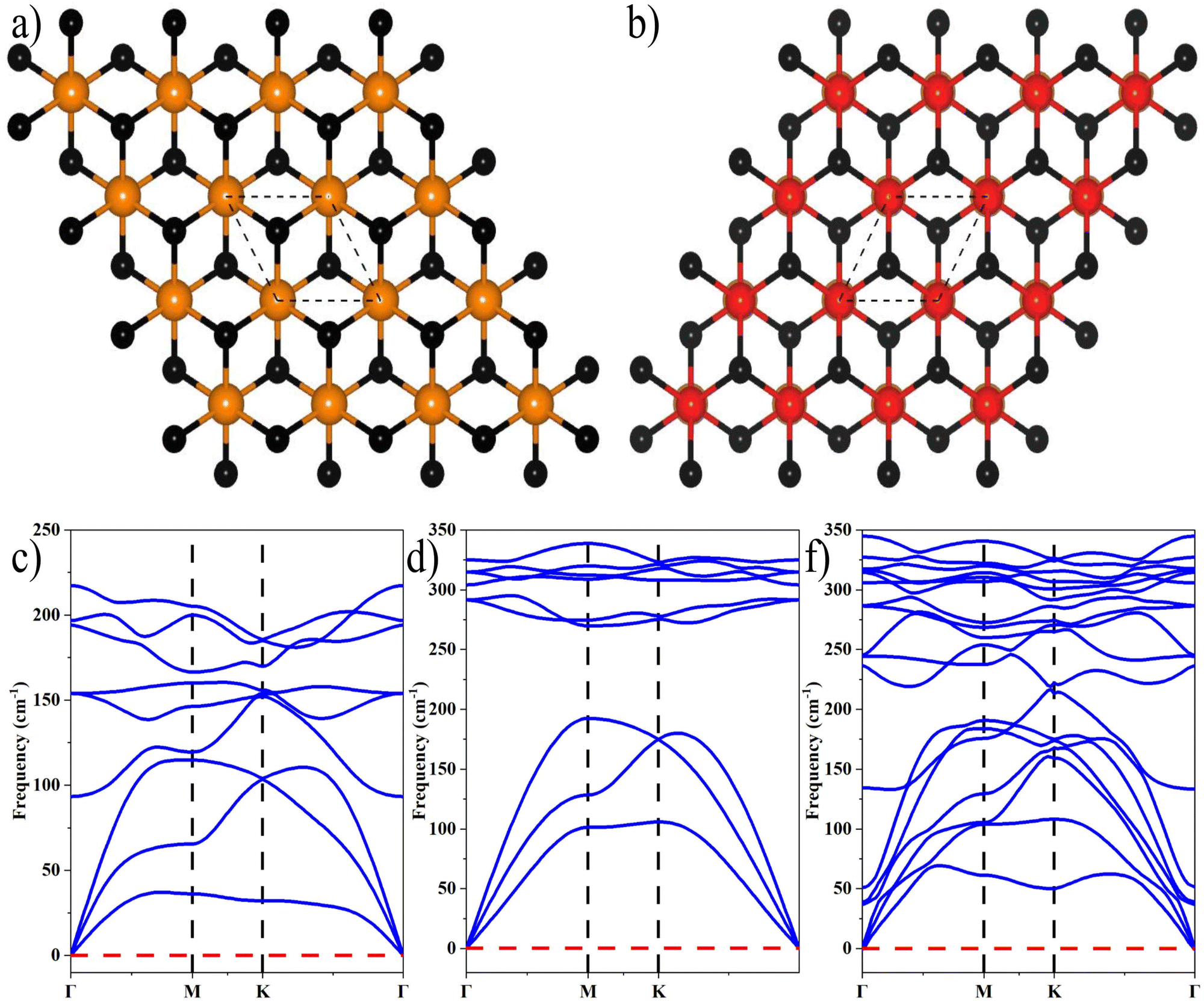
In the construction process, we have optimized the MLs PtS2 and ZrS2 to get accurate lattice parameters. It is found that both the MLs PtS2 and ZrS2 have lattice parameters of 3.58 Å and 3.68 Å respectively with a hexagonal unit cell. The bond length between the Pt–S atoms in monolayer PtS2 is 2.40 Å whereas the monolayer ZrS2 has a bond length of 2.57 Å between the Zr–S atoms. Our calculated lattice parameters of PtS2 and ZrS2 are in close agreement with previously reported data.48,49 The key parameter to construct the v-HS is lattice mismatch, which is calculated using formula (5).50| |  | (5) |
where aZrS2 and aPtS2 denote the lattice parameters of ML ZrS2 and ML PtS2, respectively. The lattice mismatch between the two considered ML PtS2 and ML ZrS2 is 2.80% which is much less than the upper limit of 5%. This calculation of lattice mismatch suggests that both the monolayers are suitable for the construction of v-HS. After this, we placed the ZrS2 monolayer on the top of the PtS2 monolayer in six different possible ways. The interlayer distance between two consecutive layers and lattice parameters of these six configurations were obtained by performing the optimization, which are listed in Table 1 along with the bond lengths, and adhesion energies whereas these six possible configurations are shown in Fig. 1(a)–(f) and the top and bottom view are shown in Fig. 2(a) and (b). The top and bottom views of v-HS of ABB1, BAB, BAB1, BBA and BBA1 are shown in Fig. S1(a–d), S2(a–d) and S3(a and b) of the ESI.† Furthermore, the negative values of adhesion energy indicate the stability of the v-HS PtS2/ZrS2 which is determined using formula (6).50| | | Eae = Ev-HS − EPtS2 − EZrS2 | (6) |
where Eae, Ev-HS, EPtS2 and EZrS2 represent the adhesion energy, energy of v-HS PtS2/ZrS2, energy of monolayer PtS2 and energy of monolayer ZrS2, respectively.
Table 1 The interlayer distance, bond length, adhesion energy, and lattice parameter
| Configurations |
Interlayer distance (Å) |
Bond length (Å) |
Adhesion energy (eV) |
Lattice parameter (Å) |
| Pt–S |
Zr–S |
| ABB |
2.82 |
2.41 |
2.56 |
−1.10 |
3.617 |
| ABB1 |
3.53 |
2.41 |
2.56 |
−1.02 |
3.614 |
| BAB |
2.96 |
2.41 |
2.56 |
−1.08 |
3.614 |
| BAB1 |
3.53 |
2.41 |
2.56 |
−1.02 |
3.613 |
| AAB |
3.00 |
2.41 |
2.56 |
−1.08 |
3.617 |
| AAB1 |
3.05 |
2.41 |
2.56 |
−1.07 |
3.616 |
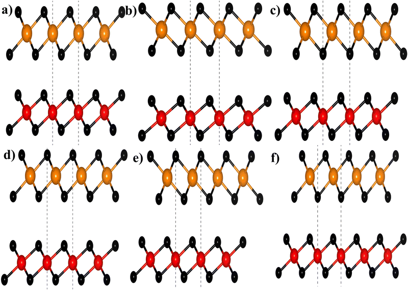 |
| | Fig. 1 Different stackings of v-HS (a) ABB, (b) ABB1, (c) BAB, (d) BAB1, (e) BBA, and (f) BBA1; here black, orange, and red balls represent the S, Zr, and Pt atoms, respectively. | |
 |
| | Fig. 2 (a) and (b) Top and bottom view of v-HS PtS2/ZrS2 respectively, and (c)–(f) the phonon dispersion relationships of MLs ZrS2, PtS2, and v-HS PtS2/ZrS2, respectively. | |
The dynamical stabilities of MLs PtS2 and ZrS2 and all the six configurations v-HS are verified using the phonon dispersion profiles and it is found that the MLs PtS2 and ZrS2 and ABB configuration of v-HS PtS2/ZrS2 possess positive phonon frequencies in the phonon dispersion profile, whereas all the other configurations of v-HS PtS2/ZrS2 have negative phonon frequencies in the phonon dispersion profile. Due to this reason, we have discarded all the other variations namely ABB1, BAB, BAB1, BBA, and BBA1. The phonon dispersion profile of MLs PtS2 and ZrS2, and the ABB configuration of v-HS PtS2/ZrS2 are shown in Fig. 2(c), (d) and (f).
Electronic properties
As ML PtS2, ML ZrS2, and v-HS PtS2/ZrS2 possess a hexagonal unit cell, the band structures of these systems are calculated along the “Γ–M–K–Γ” high symmetry path with both the PBE and HSE functional. The orbital contribution from each atom was determined using the projected density of states (PDOS) calculation. For ML PtS2, the band structure calculations reveal the indirect band gap of 1.73 eV and 2.40 eV by the PBE and HSE functional, respectively, as shown in Fig. 3(a) and (b), and the PDOS calculation shows that the p-orbital of the S atom has a significant presence in the valence band near the Fermi level, while both the d orbital of the Pt atom and the p orbital of the S atom equally contribute to the formation of the conduction band near the Fermi level, as illustrated in Fig. 3(c). For ML ZrS2, the band structure calculations with the PBE and HSE functional reveal the indirect band gap of 0.99 eV and 1.97 eV, respectively, as shown in Fig. 3(d) and (e), and the PDOS calculation shows that the p-orbital of the S atom has a significant presence in the valence band near the Fermi level while the d orbital of the Zr atom provides the major contribution in the formation of the conduction band, which is illustrated in Fig. 3(f). These obtained results of electronic band structures for ML PtS2 and ML ZrS2 are in close agreement with previously reported data.48,49 For v-HS of PtS2/ZrS2, the band structure calculations with the PBE and HSE functional reveal the indirect band gap of 0.75 eV and 1.49 eV, respectively, as shown in Fig. 3(g) and (h) while PDOS calculation is shown in Fig. 3(i), which suggests that the p-orbital of the S atom of ML PtS2 provides the major contribution in the valence band formation near the Fermi level while the conduction band near the Fermi level is mainly contributed by the d orbital of the Zr atom. The PDOS calculation of v-HS of PtS2/ZrS2 suggests that it has a staggered (type-II) band gap which is confirmed by the work function, charge density, and band alignment calculations. In our computation of electronic properties, these obtained results support the previously reported data with the PBE functional but in order to get more accurate results we have used the HSE functional.51,52
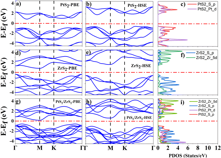 |
| | Fig. 3 (a), (d) and (g) Band structure of ML PtS2, ML ZrS2, and v-HS PtS2/ZrS2 with the PBE functional, (b), (e) and (h) band structure of ML PtS2, ML ZrS2 and v-HS PtS2/ZrS2 with the HSE functional, and (c), (f) and (i) PDOS of ML PtS2, ML ZrS2 and v-HS PtS2/ZrS2 with the HSE functional. | |
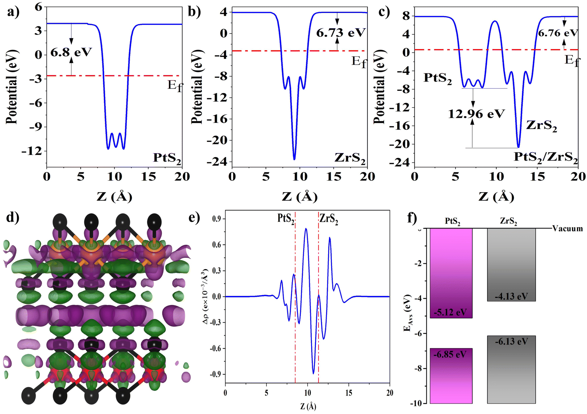
The work function of the material is defined as the amount of energy required to remove an electron from the surface, which is calculated using formula (7),53 where the terms Ef and Evac correspond to the Fermi energy and electrostatic potential relative to the vacuum, respectively, and work functions of ML PtS2, ML ZrS2, and v-HS PtS2/ZrS2 are illustrated in Fig. 4(a)–(c) respectively.
 |
| | Fig. 4 (a–c) Work functions of ML PtS2, ML ZrS2 and V-HS PtS2/ZrS2, (d) charge density difference where green and violet clouds represent the charge depletion and accumulation and also black, orange and red balls represent S, Zr, and Pt atoms, (e) average planner charge density difference, and (f) band alignment of ML PtS2 and ML ZrS2. | |
From work function calculation it is found that the ML PtS2 and ML ZrS2 possess the work function of 6.80 eV and 6.73 eV, respectively. The lower value of the work function of ML ZrS2 than ML PtS2 suggests the electron transfer from ML ZrS2 to ML PtS2. Moreover, it is also a well-known fact that the electron will always move from a lower potential region to a higher potential region. From the work function profile of v-HS, it is found that it possesses the work function of 6.76 eV with a potential difference of 12.96 eV between ML ZrS2 and ML PtS2 which drives the electron transfer from ML ZrS2 to ML PtS2.
| | | Δρ = ρv-HS − ρPtS2 − ρZrS2 | (8) |
The charge density difference (CDD) is calculated using formula (8),53 where the mathematical notations ρv-HS, ρPtS2, and ρZrS2 represent the charge densities of v-HS of PtS2/ZrS2, ML PtS2, and ML ZrS2 respectively. The CDD along with the average planner charge density is illustrated in Fig. 4(d) and (e). In Fig. 4(d) the violet clouds over the ML PtS2 represent the charge accumulation and green clouds below the ML ZrS2 represent the charge depletion which suggests significant charge transfer from ML ZrS2 to ML PtS2. From the average planar density which is illustrated in Fig. 4(e), it can be seen that at the interface the negative value of the average planner density near the ML ZrS2 and positive value near the ML PtS2 suggests the charge transfer from ML ZrS2 to ML PtS2. The exact amount of electron transfer is calculated using Löwdin population charge analysis, which is found to be 0.212 electrons transfer from ML ZrS2 to ML PtS2.
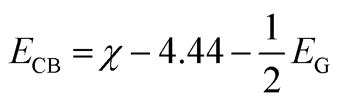
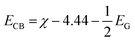
Finally, the type-II band gap of PtS2/ZrS2 was confirmed by the band alignment calculations which were calculated using eqn (9)–(11).54 The band gap of the HSE functional was used to calculate the band alignment. The band alignment is shown in Fig. 4(f).
| |  | (9) |
where
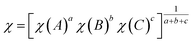
The given eqn (9)–(11) involve several variables, including χ, ECB, EVB, and EG, which represent absolute electron negativity, the position of the conduction band edge in the normal hydrogen electrode (NHE) scale, the position of the valence band in the NHE scale, and the band gap of the semiconductor, respectively. The values of ECB and EVB are obtained in the NHE scale, and eqn (11) is used to convert these values to the absolute vacuum scale (AVS).
Impact of biaxial strain on v-HS PtS2/ZrS2
We have applied compressive and tensile biaxial strain of 3% to the v-HS of PtS2/ZrS2. On the application of compressive strain of 3% the interlayer distance increases from 2.82 Å to 2.85 Å, whereas on the application of tensile strain, the interlayer distance between two consecutive layers decreases from 2.82 Å to 2.80 Å. The band gap of v-HS decreases on the application of compressive strain whereas it increases on the application of tensile strain. The effects of strain on the interlayer distance, bond length, and bandgap are summarized in Table 2.
Table 2 The impact of biaxial strain on interlayer distance, bond lengths, and bandgap (HSE)
| Strain |
Interlayer distance (Å) |
Bond length (Å) |
Band-gap (eV) |
| Pt–S |
Zr–S |
| Compressive |
−3 |
2.856 |
2.38 |
2.52 |
1.34 |
| −2 |
2.848 |
2.39 |
2.53 |
1.38 |
| −1 |
2.835 |
2.40 |
2.55 |
1.42 |
| Unstrained |
0 |
2.826 |
2.41 |
2.56 |
1.49 |
| Tensile |
1 |
2.821 |
2.42 |
2.57 |
1.53 |
| 2 |
2.816 |
2.43 |
2.58 |
1.54 |
| 3 |
2.801 |
2.44 |
2.59 |
1.55 |
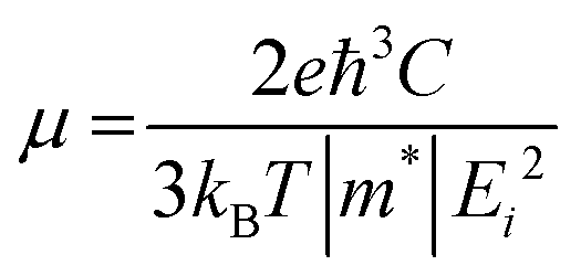
Carrier mobility
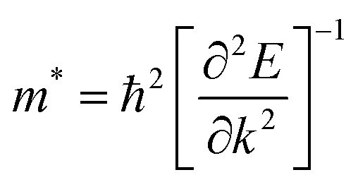
By comparing the mobility of electrons and holes, it is possible to obtain information about the lifetime and recombination of photo-generated carriers. To obtain an overall picture instead of directional-dependent mobility, we have computed the average carrier mobility for both electrons and holes. The determination of carrier mobility is achieved by employing Bardeen and Shockley's deformation potential theory based on the effective mass approximation, which is given by eqn (12).55,56| | 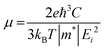 | (12) |
where e, ℏ, C, kB, and T denote the elementary charge, the reduced plank constant, the elastic modulus, the Boltzmann constant, and the temperature. Moreover m* is the effective mass, which is calculated using the formula (13) and obtained by quadratic polynomial curve fitting while Ei represents the deformation potential calculated using formula (14)| | 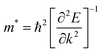 | (13) |
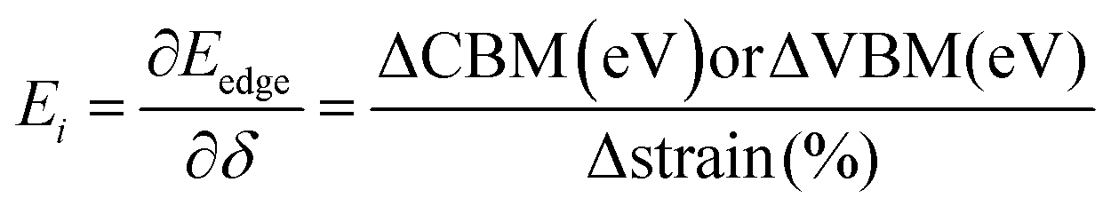
| |  | (14) |
where ΔCBM and ΔVBM represent the change in the conduction band and change in the valence band with respect to applied strain, respectively. The calculated values are summarized in Table 3.
Table 3 Effective mass, deformation potential, elastic modulus, and carrier mobility of v-HS PtS2/ZrS2
| Charge |
Effective mass (units of me) |
Deformation potential (eV) |
Elastic modulus (N m−1) |
Carrier mobility (m2 V−1 s−1) |
| Hole |
0.62 |
13.86 |
156.25 |
0.0063 |
| Electron |
0.37 |
10.07 |
0.033 |
Earlier, it was mentioned that the type-II band gap confines the electron and the hole in different monolayers, resulting in a lower recombination rate. This effect is supported by the carrier mobility values, which indicate that the mobility of the hole is significantly lower than that of the electron. This lower mobility of the hole contributes to the reduced recombination rate.
Optical properties
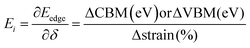
The 2D systems have the confinement of electrons in an out-of-plane direction and thus electrons can only move in in-plane directions. Due to this reason, we have individually studied the optical response of all the considered 2D systems in both in-plane and out-of-plane directions using the complex dielectric function.57 The real part of the complex dielectric function describes how a material's polarizability changes when it is exposed to an oscillating electric field of EM waves. Fig. 5(a) and (b) show the real part of the dielectric constant for the in-plane and out-of-plane components of ML PtS2, ML ZrS2, and v-HS PtS2/ZrS2, respectively. From Fig. 5(a), we can observe that the static dielectric constant values for the in-plane components of ML PtS2, ML ZrS2, and v-HS PtS2/ZrS2 are 4.47, 4.01, and 8.43, respectively. Similarly, the static dielectric constant values for the out-of-plane components of these materials are found to be 1.46, 1.48, and 2.05, respectively. The enhancement of the static dielectric constant in both the in-plane and out-of-plane components of ε1(ω) suggests lower exciton binding energy as a result of effective separation of electrons and holes in v-HS PtS2/ZrS2. Additionally, in-plane components of ML PtS2, ML ZrS2, and v-HS PtS2/ZrS2 exhibit negative values of ε1(ω) around 4.21 eV, 3.21 eV, and 3.23 eV, respectively, which signifies the metallic behavior at those frequencies. In contrast, out-of-plane components of ML PtS2, ML ZrS2, and v-HS PtS2/ZrS2 do not exhibit negative values of ε1(ω), which signifies the semiconducting behavior of these materials in the entire EM spectrum. The imaginary part of the dielectric constant is associated with the interband transition and absorption, which is illustrated in Fig. 5(c) and (d) along with its in-plane and out-of-plane components. In ML PtS2, the peaks of ε2(ω) were observed around 3.01 eV, and similarly in ML ZrS2 and v-HS PtS2/ZrS2 the peaks of ε2(ω) at 2.71 eV signify the interband transition in their respective systems. All three considered systems ML PtS2, ML ZrS2, and v-HS PtS2/ZrS2 have the highest peaks in the visible region of the EM spectrum suggesting that absorption starts from the visible region of the EM spectrum. The out-of-plane component of ML PtS2, ML ZrS2, and v-HS PtS2/ZrS2 shows very minimal changes compared to in-plane components.
 |
| | Fig. 5 (a) In-plane components of the real part of the ML PtS2, ML ZrS2 and v-HS PtS2/ZrS2, (b) out-of-plane components of the real part of the ML PtS2, ML ZrS2 and v-HS PtS2/ZrS2, (c) in-plane components of the imaginary part of the ML PtS2, ML ZrS2 and v-HS PS2/ZrS2, and (d) out-of-plane components of the imaginary part of the ML PtS2, ML ZrS2, and v-HS PtS2/ZrS2. | |
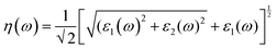
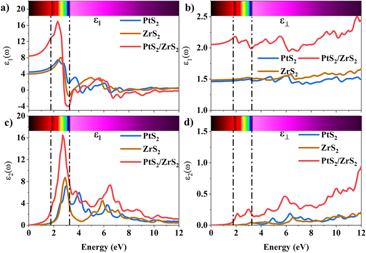
The K(ω) represents the rate of photon absorption at a particular energy, which is illustrated by Fig. 6(a) and (b). Comparing the in-plane component of the K(ω) spectrum of ML PtS2 and ML ZrS2 shows that they both exhibit peaks at 3.01 eV, while ML PtS2 also has additional peaks at 2.32 eV, 4.12 eV and 6.43 eV, and ML ZrS2 has an additional peak at 5.92 eV. On the other hand, the in-plane component of the K(ω) spectrum of v-HS PtS2/ZrS2 shows a peak at 2.91 eV, which is similar to those of ML PtS2 and ML ZrS2, respectively, but it also has a new peak at 6.63 eV. The peaks observed in the in-plane component of the K(ω) spectrum indicate that at these specific frequencies, the photons have the shortest penetration depth (δ = c/2πωK). The penetration depth refers to the distance at which the intensity of the photons reduces to 1/e or 37% of their value at the surface. The penetration depth in v-HS PtS2/ZrS2 is found to be 3.66 nm and 2.32 nm for the peak values of 2.91 eV, and 6.63 eV, respectively. The K(ω) spectrum of the out-of-plane component shows very negligible values for ML PtS2, ML ZrS2, and v-HS PtS2/ZrS2. The amount of bending that occurs in EM waves can be determined by examining the η(ω) spectrum, which is displayed in Fig. 6(c, d). By analyzing Fig. 6(c), it is seen that the static refractive indices for the in-plane components of ML PtS2, ML ZrS2, and v-HS PtS2/ZrS2 are 2.11, 2.00, and 2.90, respectively. Similarly, the refractive indices for the out-of-plane components of these materials are found to be 1.20, 1.21, and 1.43, respectively. The in-plane component of the η(ω) spectrum for ML PtS2 exhibits a peak at 2.41 eV, which then gradually decreases until it reaches 5.05 eV, after which it shows only minimal changes. Similarly, the in-plane component of the η(ω) spectrum for ML ZrS2 displays a peak at 2.61 eV, which also steadily decreases until it reaches 7.53 eV and then shows minimal changes. Additionally, the in-plane component of the η(ω) spectrum for v-HS PtS2/ZrS2 reaches a peak at 2.31 eV, after which it gradually decreases until it reaches 7.43 eV, and then shows minimal changes. The out-of-plane component of the η(ω) spectrum for ML PtS2, ML ZrS2, and v-HS PtS2/ZrS2 displays minimal changes across the EM spectrum.
 |
| | Fig. 6 (a) In-plane components of K(ω) of the ML PtS2, ML ZrS2 and v-HS PtS2/ZrS2, (b) out-of-plane components of K(ω) of the ML PtS2, ML ZrS2 and v-HS PtS2/ZrS2, (c) in-plane components of η(ω) of the ML PtS2, ML ZrS2 and v-HS PtS2/ZrS2, (d) out-of-plane components of η(ω) of the ML PtS2, ML ZrS2 and v-HS PtS2/ZrS2. | |
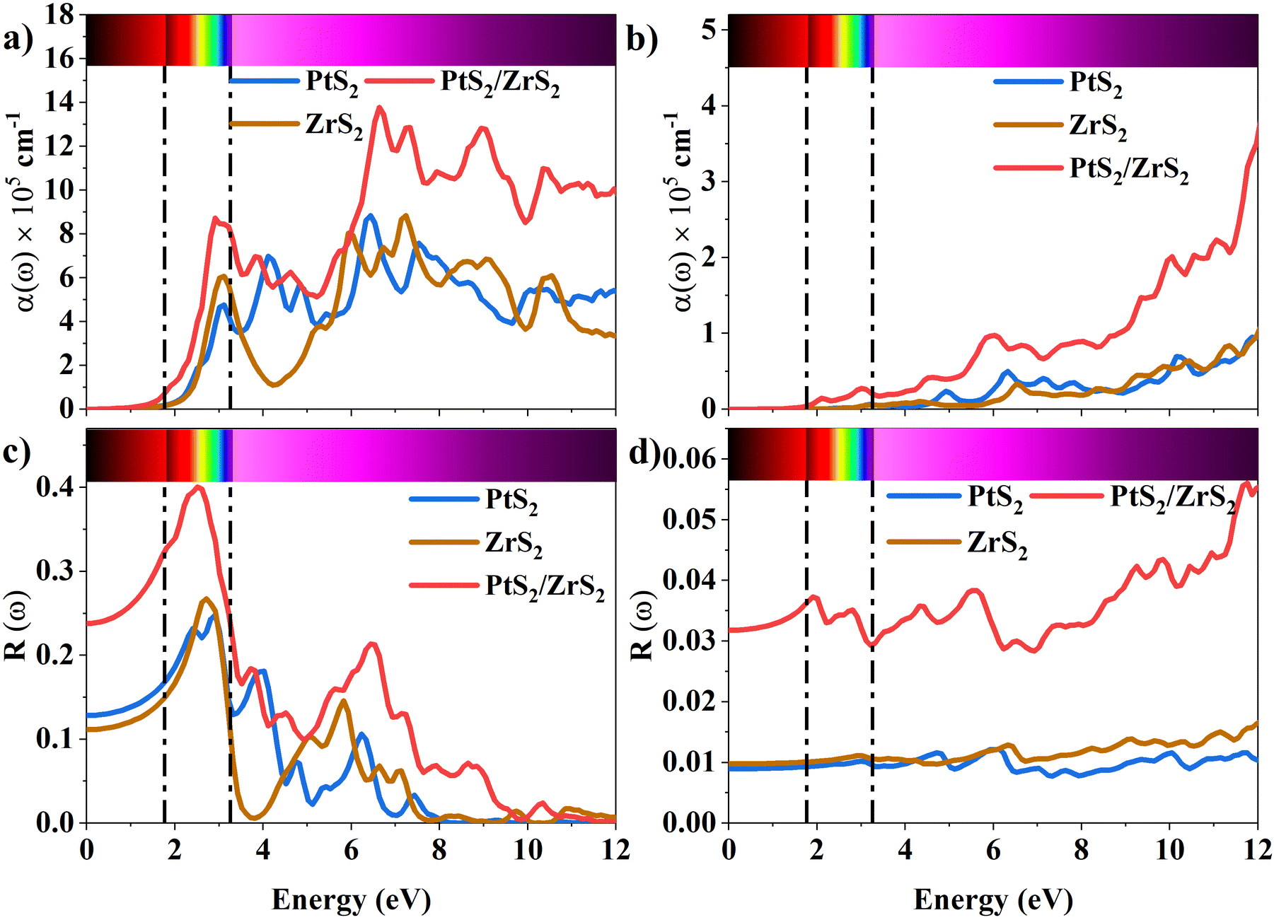
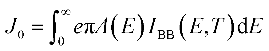
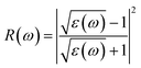
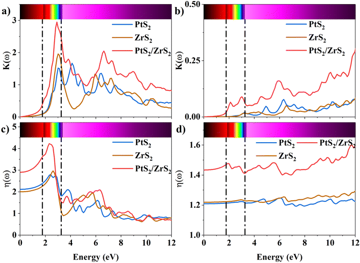
The absorption coefficient is a measure of the distance an electron can travel without being fully absorbed. The in-plane and out-of-plane components of the absorption coefficient are shown in Fig. 7(a) and (b). In the in-plane component of the absorption coefficient spectrum for ML PtS2, peaks are observed at 3.11 eV, 4.12 eV, 4.82 eV, and 6.43 eV. Similarly, for ML ZrS2, peaks are observed at 3.11 eV, 5.92 eV, and 7.23 eV, and for v-HS PtS2/ZrS2, peaks are observed at 2.91 eV, 6.63 eV, and 8.94 eV. On the other hand, in the out-of-plane component of the absorption coefficient spectrum, only a small peak is observed at 6.33 eV for ML PtS2, and a small peak is observed at 6.53 eV for ML ZrS2. However, for v-HS PtS2/ZrS2, there is a steady increase observed across the EM spectrum in the out-of-plane component of the absorption coefficient spectrum. Furthermore, both the in-plane and out-of-plane components of the absorption coefficient for v-HS exhibit enhanced absorption across the entire EM spectrum. Reflectivity is a measure of how much light or electromagnetic radiation is reflected from a surface. The in-plane and out-of-plane components of reflectivity are shown in Fig. 7(c) and (d). The EM spectrum of Reflectivity shows that the in-plane components of ML PtS2 and ML ZrS2 have the highest reflectivity of 24% at 2.91 eV, and 26% at 2.71 eV respectively, whereas v-HS PtS2/ZrS2 exhibits an enhanced reflectivity of 40% at 2.61 eV. However, after reaching the peak value, the reflectivity of all three materials sharply decreases in the visible and UV regions of the EM spectrum. On the other hand, the out-of-plane component of ML PtS2 and ML ZrS2 has the highest reflectivity of 1.2% at 6.13 eV, and 1.6% at 11.95 eV. In contrast, v-HS PtS2/ZrS2 has the highest reflectivity of 5.6% at 11.75 eV.
 |
| | Fig. 7 (a) In-plane components of α(ω) of the ML PtS2, ML ZrS2 and v-HS PtS2/ZrS2, (b) out-of-plane components α(ω) of the ML PtS2, ML ZrS2 and v-HS PtS2/ZrS2, (c) in-plane components of R(ω) of the ML PtS2, ML ZrS2 and v-HS PtS2/ZrS2, (d) out-of-plane components of R(ω) of the ML PtS2, ML ZrS2 and v-HS PtS2/ZrS2. | |
The optical band gap is calculated using formula (15) where α is absorption co-efficient, hϑ is photon energy, A is a constant, Eop is optical absorption energy and we have used n = ½ for an indirect band material.
Fig. 8 represents the Tauc plot of v-HS PtS2/ZrS2, and from the Tauc plot analysis it is found that the v-HS PtS2/ZrS2 has an optical band gap of 1.39 eV. This obtained optical band gap is very near to the our calculated HSE band gap of 1.49 eV which validates the use of the HSE functional in band structure calculation.
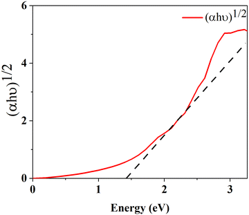 |
| | Fig. 8 Optical band gap using Tauc plot. | |
Application as a photovoltaic device
As our considered system v-HS PtS2/ZrS2 has a band gap of 1.49 eV it motivated us to study v-HS PtS2/ZrS2 as an absorber layer for photovoltaic applications. Therefore, we have determined the solar parameters, including short-circuit current density (Jsc), open-circuit voltage (Voc), fill factor (FF), and power conversion efficiency, by applying the Shockley–Queisser (SQ) limit.58 All the solar parameters are calculated using eqn (16)–(20).59,60| | 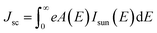 | (16) |
| |  | (17) |
| |  | (18) |
| |  | (19) |
| |  | (20) |
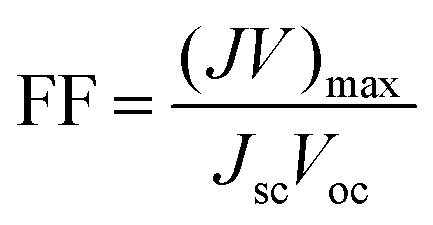
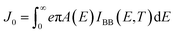
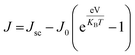
where, A(E) = 1 − e−2α(E)L and Pmout = JV
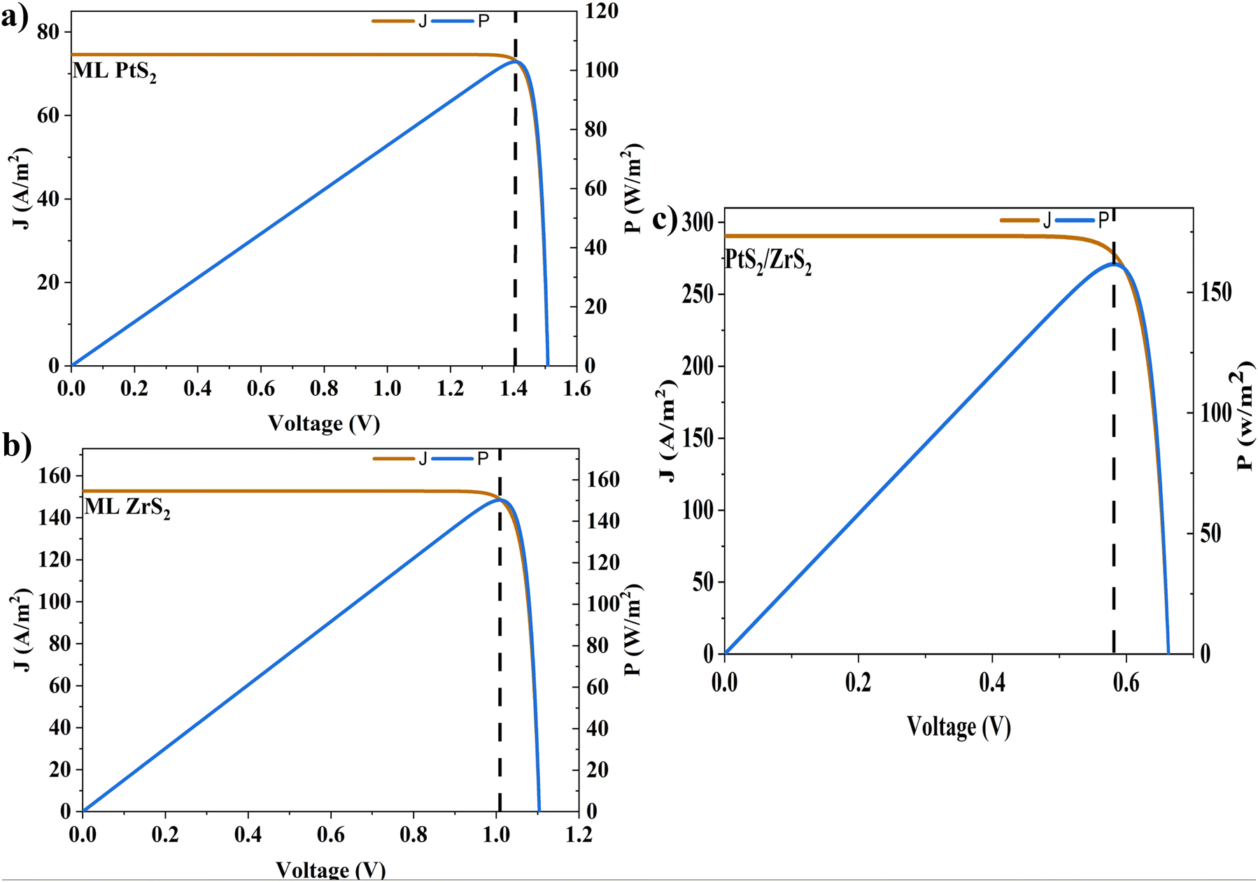
In the above equations, A(E) represents the absorptivity of the material, α(E) is the absorption coefficient, L is the thickness of the material, and Isun represents the photon flux density which is obtained from the AM1.5G solar spectrum. J0 is the reverse current density, J is the total current density, and IBB is the black-body spectrum calculated at 300 K. KB is the Boltzmann constant. V is the applied voltage. Pmout represents the maximum output power and Pin = 1000 W m−2 is the total incident power. The calculated values of ML PtS2, ML ZrS2, and v-HS PtS2/ZrS2 are summarized in Table 4. Fig. 9 represents the J–V characteristics and power density of ML PtS2, ML ZrS2, and PtS2/ZrS2.
Table 4 Solar parameters: short-circuit current density (Jsc), reverse current density (J0), open-circuit voltage (Voc), maximum output power (Pm-out), fill factor (FF), and power conversion efficiency (η)
| Material |
J
sc (A m−2) |
J
0 (A m−2) |
V
oc (V) |
P
m-out (W m−2) |
FF |
η (%) |
| ML PtS2 |
74.58 |
3.14 × 10⁻²⁴ |
1.50 |
102.6 |
0.91 |
10.26 |
| ML ZrS2 |
152.68 |
4.31 × 10⁻¹⁷ |
1.10 |
150.17 |
0.89 |
15.01 |
| v-HS PtS2/ZrS2 |
290.32 |
2.11 × 10⁻⁹ |
0.66 |
161.60 |
0.84 |
16.16 |
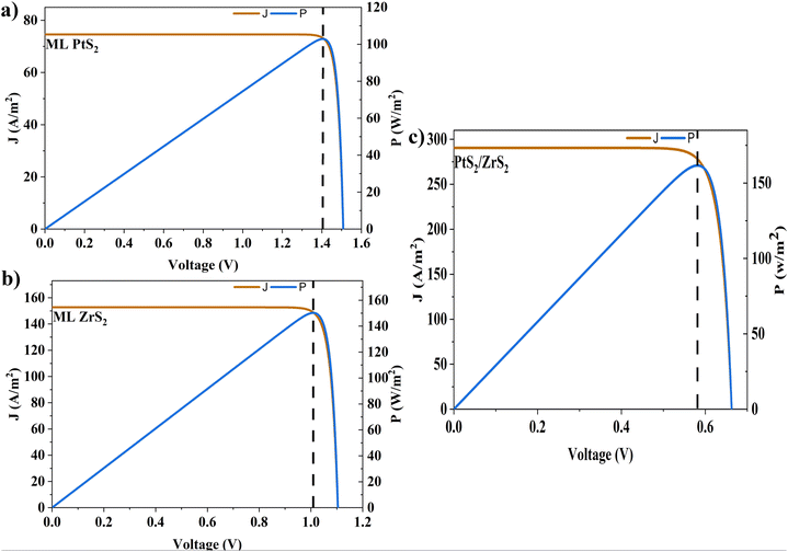 |
| | Fig. 9 (a)–(c) J–V characteristics and power density of ML PtS2, ML ZrS2, and PtS2/ZrS2. | |
Due to high bandgaps, the ML PtS2 and ML ZrS2 have low Jsc and high Voc, which is responsible for the reduction in Pm-out and η. On the contrary, the v-HS PtS2/ZrS2 possesses a moderate bandgap, which provides a balance between the Jsc and Voc and as a result we get enhancement in Pm-out and η. The values of reverse saturation current density remain negligible for the ML PtS2, ML ZrS2, and v-HS PtS2/ZrS2. The values of FF are found to be 0.91, 0.81 and 0.84 for ML PtS2, ML ZrS2, and v-HS PtS2/ZrS2, respectively.
Conclusion
In the present work, we have studied the v-HS PtS2/ZrS2 by employing DFT. The optimization of v-HS PtS2/ZrS2 reveals that it possesses a hexagonal unit cell with a lattice parameter of 3.62 Å and interlayer distance of 2.82 Å. The electronic properties are computed with the HSE functional, which reveals that the v-HS PtS2/ZrS2 possesses an indirect gap of 1.49 eV. From PDOS analysis of v-HS PtS2/ZrS2, we have concluded that the p-orbital of the S atom of ML PtS2 provides the major contribution in the valence band formation near the Fermi level while the conduction band near the Fermi level was mainly contributed by the d orbital of the Zr atom. This analysis of PDOS suggests the type-II band nature of v-HS PtS2/ZrS2, which is confirmed by the work function, charge density difference, average planar charge density, and band edge calculations. Moreover, from the Löwdin charge analysis, it is concluded that there is a transfer of 0.212 e− from ML ZrS2 to ML PtS2. From the carrier mobility calculation of V-HS PtS2/ZrS2, it is concluded that holes have less mobility compared to the electrons which demonstrates the lower recombination rate in v-HS PtS2/ZrS2. From the absorption–coefficient calculation, it is concluded that the v-HS PtS2/ZrS2 has an enhanced absorption coefficient which starts from the visible region and attains its peak value in the ultraviolet region of the EM spectrum. Moreover, we have also checked the performance of v-HS PtS2/ZrS2 for photovoltaic solar cells and it is found that it has a power conversion efficiency of 16.16%. From these results, it is concluded that v-HS PtS2/ZrS2 has potential applications in photovoltaic solar cells as well as in optoelectronic devices.
Author contributions
P. R. P.: conceptualization, data curation, formal analysis, investigation, methodology, resources, software, visualization, writing – original draft; S. J. K.: conceptualization, data curation, writing – review & editing; D. M.: conceptualization, data curation, writing – review & editing; Y. S.: conceptualization, data curation, formal analysis, investigation, software, methodology, project administration, validation, resources, writing – review & editing; P. B. T.: conceptualization, data curation, formal analysis, investigation, methodology, validation, project administration, resources, supervision, writing – review & editing.
Conflicts of interest
There are no conflicts to declare.
References
- M. Chhowalla, H. S. Shin, G. Eda, L. J. Li, K. P. Loh and H. Zhang, Nat. Chem., 2013, 5, 263–275 CrossRef PubMed.
- N. Modi, Y. Naik, P. R. Parmar, P. H. Jariwala, D. B. Shah and P. B. Thakor, Mater. Today: Proc., 2023 DOI:10.1016/j.matpr.2023.01.344.
- Y. Naik, D. Mehta, P. R. Parmar, P. H. Jariwala and P. B. Thakor, Mater. Today Proc., 2023, 1–4 Search PubMed.
- D. Mehta, N. Modi, S. J. Khengar, P. H. Jariwala and P. B. Thakor, Mater. Today Proc., 2023, 2–5 Search PubMed.
- S. J. Khengar, P. R. Parmar and P. B. Thakor, Mater. Today Proc., 2022, 67, 259–262 CrossRef CAS.
- L. Li, T. Huang, K. Liang, Y. Si, J. C. Lian, W. Q. Huang, W. Hu and G. F. Huang, Phys. Rev. Appl., 2022, 18, 1 Search PubMed.
- M. H. Dalsaniya, T. K. Gajaria, N. N. Som, P. K. Jha, P. Śpiewak and K. J. Kurzydłowski, Sol. Energy, 2021, 223, 87–99 CrossRef CAS.
-
P. R. Parmar, S. J. Khengar and P. B. Thakor DOI:10.1016/j.matpr.2022.06.011.
- A. Patel, D. Singh, Y. Sonvane, P. B. Thakor and R. Ahuja, Mater. Today Proc., 2020, 47, 526–528 CrossRef.
- A. O. M. Almayyali, B. B. Kadhim and H. R. Jappor, Phys. E, 2020, 118, 113866 CrossRef CAS.
- S. Wang, H. Tian, C. Ren, J. Yu and M. Sun, Sci. Rep., 2018, 6–11 Search PubMed.
- A. Rawat, R. Ahammed, N. Jena, M. K. Mohanta and A. De Sarkar, J. Phys. Chem. C, 2019, 123, 12666–12675 CrossRef CAS.
- K. Liang, T. Huang, K. Yang, Y. Si, H. Y. Wu, J. C. Lian, W. Q. Huang, W. Y. Hu and G. F. Huang, Phys. Rev. Appl., 2021, 16, 1 Search PubMed.
- H. C. Diaz, R. Chaghi, Y. Ma and M. Batzill, 2D Mater., 2015, 2, 44010 CrossRef.
- M. B. Alemayehu, K. Ta, M. Falmbigl and D. C. Johnson, J. Am. Chem. Soc., 2015, 137, 4831–4839 CrossRef CAS PubMed.
- K. S. Novoselov, A. Mishchenko, A. Carvalho and A. H. Castro Neto, Science, 2016, 353 DOI:10.1126/science.aac9439.
- C. V. Nguyen, Superlattices Microstruct., 2018, 116, 79–87 CrossRef CAS.
- D. Pierucci, H. Henck, J. Avila, A. Balan, C. H. Naylor, G. Patriarche, Y. J. Dappe, M. G. Silly, F. Sirotti, A. T. C. Johnson, M. C. Asensio and A. Ouerghi, Nano Lett., 2016, 16, 4054–4061 CrossRef CAS PubMed.
- D. S. Koda, F. Bechstedt, M. Marques and L. K. Teles, J. Phys. Chem. C, 2017, 121, 3862–3869 CrossRef CAS.
- Q. Peng, Z. Wang, B. Sa, B. Wu and Z. Sun, ACS Appl. Mater. Interfaces, 2016, 8, 13449–13457 CrossRef CAS PubMed.
- T. V. Vu, N. V. Hieu, L. T. P. Thao, N. N. Hieu, H. V. Phuc, H. D. Bui, M. Idrees, B. Amin, L. M. Duc and C. V. Nguyen, Phys. Chem. Chem. Phys., 2019, 21, 22140–22148 RSC.
- X. Zhou, N. Zhou, C. Li, H. Song, Q. Zhang, X. Hu, L. Gan, H. Li, J. Lü, J. Luo, J. Xiong and T. Zhai, 2D Mater., 2017, 4 DOI:10.1088/2053-1583/aa6422.
- Y. C. Rao, S. Yu and X. M. Duan, Phys. Chem. Chem. Phys., 2017, 19, 17250–17255 RSC.
- J. Shi, Y. Ou, M. A. Migliorato, H. Wang, H. Li, Y. Zhang, Y. Gu and M. Zou, Comput. Mater. Sci., 2019, 160, 301–308 CrossRef CAS.
- X. Gao, Y. Shen, Y. Ma, S. Wu and Z. Zhou, J. Mater. Chem. C, 2019, 7, 4791–4799 RSC.
- G. Wang, L. Zhang, Y. Li, W. Zhao, A. Kuang, Y. Li, L. Xia, Y. Li and S. Xiao, J. Phys. D: Appl. Phys., 2020, 53, 0–6 Search PubMed.
- D. D. Vo, V. T. T. Vi, T. P. Dao, T. V. Vu, H. V. Phuc, N. N. Hieu, N. T. T. Binh and C. V. Nguyen, Phys. E, 2020, 120 DOI:10.1016/j.physe.2020.114050.
- J. Lu, X. Zhang, G. Su, W. Yang, K. Han, X. Yu, Y. Wan, X. Wang and P. Yang, Mater. Today Phys., 2021, 18 DOI:10.1016/j.mtphys.2021.100376.
- M. Zhang, Y. Zhu, X. Wang, Q. Feng, S. Qiao, W. Wen, Y. Chen, M. Cui, J. Zhang, C. Cai and L. Xie, J. Am. Chem. Soc., 2015, 137, 7051–7054 CrossRef CAS PubMed.
- L. H. Zeng, S. H. Lin, Z. J. Li, Z. X. Zhang, T. F. Zhang, C. Xie, C. H. Mak, Y. Chai, S. P. Lau, L. B. Luo and Y. H. Tsang, Adv. Funct. Mater., 2018, 28, 1–11 Search PubMed.
- G. Liu, Y. Gan, R. Quhe and P. Lu, Chem. Phys. Lett., 2018, 709, 65–70 CrossRef CAS.
- H. Y. Lv, W. J. Lu, D. F. Shao, H. Y. Lu and Y. P. Sun, J. Mater. Chem. C, 2016, 4, 4538–4545 RSC.
- Q. Zhao, Y. Guo, K. Si, Z. Ren, J. Bai and X. Xu, Phys. Status Solidi B, 2017, 254 DOI:10.1002/pssb.201700033.
- J. Du, P. Song, L. Fang, T. Wang, Z. Wei, J. Li and C. Xia, Appl. Surf. Sci., 2018, 435, 476–482 CrossRef CAS.
- Y. Li, J. Kang and J. Li, RSC Adv., 2014, 4, 7396–7401 RSC.
- P. Giannozzi, S. Baroni, N. Bonini, M. Calandra, R. Car, C. Cavazzoni, D. Ceresoli, G. L. Chiarotti, M. Cococcioni, I. Dabo, A. Dal Corso, S. De Gironcoli, S. Fabris, G. Fratesi, R. Gebauer, U. Gerstmann, C. Gougoussis, A. Kokalj, M. Lazzeri, L. Martin-Samos, N. Marzari, F. Mauri, R. Mazzarello, S. Paolini, A. Pasquarello, L. Paulatto, C. Sbraccia, S. Scandolo, G. Sclauzero, A. P. Seitsonen, A. Smogunov, P. Umari and R. M. Wentzcovitch, J. Phys.: Condens. Matter, 2009, 21 DOI:10.1088/0953-8984/21/39/395502.
- W. Kohn, A. D. Becke and R. G. Parr, J. Phys. Chem., 1996, 100, 12974–12980 CrossRef CAS.
- G. Kresse and J. Furthmüller, Phys. Rev. B: Condens. Matter Mater. Phys., 1996, 54, 11169–11186 CrossRef CAS PubMed.
- J. P. Perdew, K. Burke and M. Ernzerhof, Phys. Rev. Lett., 1996, 77, 3865–3868 CrossRef CAS PubMed.
- S. Grimme, J. Antony, S. Ehrlich and H. Krieg, J. Chem. Phys., 2010, 132 DOI:10.1063/1.3382344.
- Hendrik J. Monkhorst and J. D. Pack, Phys. Rev. B: Solid State, 1976, 13, 5188–5192 CrossRef.
- J. Heyd, G. E. Scuseria and M. Ernzerhof, J. Chem. Phys., 2003, 118, 8207–8215 CrossRef CAS.
- G. Pizzi, V. Vitale, R. Arita, S. Blügel, F. Freimuth, G. Géranton, M. Gibertini, D. Gresch, C. Johnson, T. Koretsune, J. Ibañez-Azpiroz, H. Lee, J. M. Lihm, D. Marchand, A. Marrazzo, Y. Mokrousov, J. I. Mustafa, Y. Nohara, Y. Nomura, L. Paulatto, S. Poncé, T. Ponweiser, J. Qiao, F. Thöle, S. S. Tsirkin, M. Wierzbowska, N. Marzari, D. Vanderbilt, I. Souza, A. A. Mostofi and J. R. Yates, J. Phys. Condens. Matter, 2020, 32 DOI:10.1088/1361-648X/ab51ff.
- A. Marini, C. Hogan, M. Grüning and D. Varsano, Comput. Phys. Commun., 2009, 180, 1392–1403 CrossRef CAS.
- D. R. Hamann, Phys. Rev. B: Condens. Matter Mater. Phys., 2013, 88, 1–10 CrossRef.
- E. E. Salpeter and H. A. Bethe, Phys. Rev., 1951, 84, 1232–1242 CrossRef.
- H. R. Mahida, D. Singh, Y. Sonvane, S. K. Gupta and P. B. Thakor, Solid State Commun., 2017, 252, 22–28 CrossRef CAS.
- W. L. Tao, Y. Mu, C. E. Hu, Y. Cheng and G. F. Ji, Philos. Mag., 2019, 99, 1025–1040 CrossRef CAS.
- T. V. Vu, H. D. Tong, D. P. Tran, N. T. T. Binh, C. V. Nguyen, H. V. Phuc, H. M. Do and N. N. Hieu, RSC Adv., 2019, 9, 41058–41065 RSC.
- D. Singh and R. Ahuja, ACS Appl. Energy Mater., 2022, 5, 2300–2307 CrossRef CAS.
- R. A. B. Villaos, C. P. Crisostomo, Z. Q. Huang, S. M. Huang, A. A. B. Padama, M. A. Albao, H. Lin and F. C. Chuang, npj 2D Mater. Appl., 2019, 3, 1–8 CrossRef CAS.
- M. Kashif, N. Anjum, A. Shahzad, A. Rasheed, M. Imran and A. Manzoor, ACS Omega, 2022, 7, 33453–33460 CrossRef CAS PubMed.
- F. Opoku, S. O.-B. Oppong, N. K. Asare-Donkor, O. Akoto and A. A. Adimado, Energy Adv., 2022, 1, 146–158 RSC.
- M. M. Obeid, A. Bafekry, S. U. Rehman and C. V. Nguyen, Appl. Surf. Sci., 2020, 534, 147607, DOI:10.1016/j.apsusc.2020.147607.
- P. Mishra, D. Singh, Y. Sonvane and R. Ahuja, Sustainable Energy Fuels, 2020, 4, 2363–2369 RSC.
- A. Patel, D. Singh, Y. Sonvane, P. B. Thakor and R. Ahuja, ACS Appl. Mater. Interfaces, 2020, 12, 46212–46219 CrossRef CAS PubMed.
- X. Yang, D. Singh, Z. Xu, Z. Wang and R. Ahuja, J. Mater. Chem. C, 2019, 7, 12312–12320 RSC.
-
M. Bercx, R. Saniz, B. Partoens and D. Lamoen, A Tribute to Norman H. March on the Occasion of his 90th Birthday, Many-body Approaches at Different Scales, 2018, pp. 177–184 Search PubMed.
- N. N. Som, V. Sharma, V. Mankad, M. L. C. Attygalle and P. K. Jha, Sol. Energy, 2019, 193, 799–805 CrossRef CAS.
- M. Bercx, N. Sarmadian, R. Saniz, B. Partoens and D. Lamoen, Phys. Chem. Chem. Phys., 2016, 18 10.1039/C6CP03468C.
|
| This journal is © The Royal Society of Chemistry and the Centre National de la Recherche Scientifique 2023 |

 a,
S. J.
Khengar
a,
Disha
Mehta
a,
Yogesh
Sonvane
a,
S. J.
Khengar
a,
Disha
Mehta
a,
Yogesh
Sonvane