DOI:
10.1039/D2TA07239D
(Paper)
J. Mater. Chem. A, 2022,
10, 24717-24725
High-performance and low-cost organic solar cells based on pentacyclic A–DA′D–A acceptors with efficiency over 16%†
Received
14th September 2022
, Accepted 7th November 2022
First published on 8th November 2022
Abstract
Developing high-performance and low-cost donor/acceptor materials is crucial for the industrialization of organic solar cells (OSCs). Therefore, a series of new donor and acceptor materials with simple structures and easy synthesis have been reported. However, how to further achieve low-cost and high-performance OSCs is still an issue that should be solved when competing with other photovoltaic technologies. Herein, we demonstrate a high-performance and low-cost PTQ10:Y26 system with an impressive efficiency of 16.01% via a series of morphology optimizations. Moreover, the devices demonstrated excellent bulk-heterojunction (BHJ) thickness tolerance over the range of 100 nm to 300 nm, which is beneficial for large-scale fabrications. Besides, we calculated the industrial figure of merit (i-FOM) of the PTQ10:Y26 system and made a relatively comprehensive comparison with other classic BHJ combinations based on A–DA′D–A acceptors. The PTQ10:Y26 system shows a high FOM of over 0.3, which is among the high FOM values for OSCs now. Combining with the merits of low cost, high efficiency and thickness insensitivity, we firmly believe that PTQ10:Y26 shows great potential in the commercialization for OSCs.
1. Introduction
As one of the third-generation solar cells, organic solar cells (OSCs) have gained wide interest in recent years because of their advantages in solution processing, flexibility, semitransparency, tunable structures, etc.1–3 In the early stage, the acceptors in bulk-heterojunction (BHJ) are mainly dominated by fullerene materials such as PCBM (phenyl-C61-butyric acid methyl ester). However, the power conversion efficiency (PCE) of fullerene-based OSCs lags far behind those of their inorganic counterparts due to the disadvantages of fullerene and its derivatives such as high energy loss (Eloss), limited light absorption, and large energy offset for charge dissociation.4 Further, a lot of small molecular acceptors (SMAs) were designed and synthesized to overcome the drawbacks of fullerene acceptors. In 2015, Zhan et al. reported the famous acceptor ITIC [(3,9-bis(2-methylene-(3-(1,1-dicyanomethylene)-indanone))-5,5,11,11-tetrakis(4-hexylphenyl)-dithieno[2,3-d:20,30-d0]-s-indaceno[1,2-b:5,6-b0]dithiophene)] with a structure of A–D–A (where A and D denote electron-withdrawing and electron-donating units, respectively); however, the insufficient short-circuit current density (Jsc) caused by the poor near-infrared absorption and high Eloss restricts the further improvement of efficiency.5 In 2019, Zou et al. reported a benchmark acceptor Y6 [(2,2′-(2Z,2′Z)-((12,13-bis(2-ethylhexyl)-3,9-diundecyl-12,13-dihydro-[1,2,5]thiadiazolo[3,4-e]thieno[2′′,3′′:4′,5′]thieno[2′,3′:4,5]pyrrolo[3,2-g]thieno[2′,3′:4,5]-thieno[3,2-b]indole-2,10-diyl)bis(methanylylidene))bis(5,6-difluoro-3-oxo-2,3-dihydro-1H-indene-2,1-diylidene))dimalononitrile)] with an A–DA′D–A structure using benzothiadiazole as the electron-deficient core, which first achieved an efficiency of over 15% and triggered a big wave of research.6 Benefitting from the innovations in material structures and device optimizations,7–10 single-junction and tandem OSCs based on A–DA′D–A acceptors, Y6 analogs, have achieved PCEs over 19% and 20%, respectively.11–21
Although tremendous progress has been made in improving the PCE, OSCs still suffer from the cost issue that needed to be solved towards industrialization in the future.22,23 A BHJ combination with easy synthesis and simple structures for achieving high PCEs is important; therefore, quite some efforts are involved in reducing the cost of chemical synthesis. Generally, decreasing synthetic steps is a common approach to reduce the cost.24 For example, Li et al. reported a new polymer donor poly[(thiophene)-alt-(6,7-difluoro-2-(2-hexyldecyloxy)quinoxaline)] (PTQ10) with relatively few synthetic steps and high overall yields. By blending with the pentacyclic acceptor IDIC, the device showed a high PCE of 12.7% with a good thickness tolerance from 100 to 300 nm, which is beneficial for large-area processing.25 Furthermore, the PTQ10 showed excellent compatibility with the Y6 acceptor, and the PCE of PTQ10:Y6 reached about 16.5% after a series of optimizations.26,27 However, another way to lower the overall cost is to reduce the synthetic steps of acceptors.28–30 In 2021, our group reported a pentacyclic A–DA′D–A acceptor Y26 yielding a PCE of 13.34% when blending with poly[(2,6-(4,8-bis(5-(2-ethylhexyl-3-fluoro)thiophen-2-yl)-benzo[1,2-b:4,5-b0] dithiophene))-alt-(5,5-(10,30-di-2-thienyl-50,70-bis(2-ethylhexyl)benzo[10,20-c:40,50-c0]dithio-phene-4,8-dione))] (PM6). This work shed light on the importance of introducing the alkyl side chain into the β position of thiophenes. The rotation of the terminal group could be restricted, and moreover, noncovalent interactions were formed, which were conducive to improving the ordered molecular packing and orientation. Besides, it was verified that Y26 decreased synthetic steps and the material synthesis cost compared to Y18 [(2,2′-((2Z,2′Z)-((6,12,13-tris(2-ethylhexyl)-3,9-diundecyl-12,13-dihydro-6H-thieno[2′′,3′′:4′,5′]thieno[2′,3′:4,5]pyrrolo[3,2-g]thieno[2′,3′:4,5]thieno[3,2-b][1,2,3]triazolo[4,5-e]indole-2,10-diyl)bis(methaneylylidene))bis(5,6-difluoro-3-oxo-2,3-dihydro-1H-indene-2,1-diylidene))dimalononitrile)]; however, this work did not assess the cost issue by a quantitative method in detail.29
The reduced fused-ring number of Y26 relative to heptacyclic acceptors such as Y6 leads to the decreased synthesis step and cost. The fly in the ointment is that the efficiency is not high enough. Thus, how to further improve the efficiency of Y26 comparable to heptacyclic acceptors is also important, because the decrease in central fused-ring number is usually accompanied by the decrease in device efficiency. Herein, we demonstrate high-performance and low-cost OSCs using pentacyclic Y26 and well-known PTQ10 as the acceptor and donor, respectively. After morphological optimization, the champion device displays an excellent efficiency of 16.01%, which is rather close to the initially reported efficiency of OSCs based on heptacyclic acceptors such as Y6. After an in-depth study, we found that the solvent vapor annealing (SVA) treatment could adjust the fine phase separation between PTQ10 and Y26 as well as increase the ordered molecular packing and the favorable orientation of Y26, which is beneficial for charge generation, dissociation, transport, and suppressing charge recombination. Besides, further investigations demonstrate that the PTQ10:Y26 device shows a high PCE of 15.02% when the BHJ thickness increases to 300 nm, indicating excellent thickness insensitivity. Moreover, the industrialized potential of PTQ10:Y26 with representative BHJ systems by calculating their industrial figure of merit (i- FOM) parameters as a comparison was analyzed, and then we found that PTQ10:Y26 had a higher i-FOM value than others. These findings indicated that PTQ10:Y26 could be one of the more viable choices for OSC industrialization and also provided some guidelines for accelerating the practical applications of OSCs in the future.
2. Results and discussion
2.1 Chemical structure and absorption spectra of PTQ10 and Y26
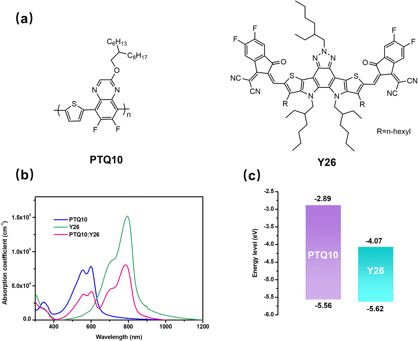
The chemical structures of the PTQ10 donor and Y26 acceptor are shown in Fig. 1a. In addition, Fig. S1† plots the solution absorption spectra of PTQ10, Y26, and their mixture (w/w, 1![[thin space (1/6-em)]](https://www.rsc.org/images/entities/char_2009.gif) :1.2) in chloroform (CF). The absorption spectra of the PTQ10, Y26, and PTQ10:Y26 films are shown in Fig. 1b. Y26 shows broad and complementary absorption in the range of 650 to 850 nm with a maximum absorption peak at 796 nm, whereas PTQ10 displays strong absorption ranging from 300 to 650 nm. Furthermore, the cyclic voltammetry (CV) measurement was used to estimate the energy levels of PTQ10 and Y26. Their energy level alignments are given in Fig. 1c and S2† displays the complete CV curves. The calculated highest occupied molecular orbital (HOMO)/lowest unoccupied molecular orbital (LUMO) levels of PTQ10 and Y26 were found to be −5.56 eV/−2.89 eV and −5.62 eV/−4.07 eV, respectively. Besides, the modest HOMO offset (ΔEHOMO) of 0.06 eV between PTQ10 and Y26 contributes to improving open-circuit voltage (Voc) while simultaneously providing enough driving force for exciton separation.
:1.2) in chloroform (CF). The absorption spectra of the PTQ10, Y26, and PTQ10:Y26 films are shown in Fig. 1b. Y26 shows broad and complementary absorption in the range of 650 to 850 nm with a maximum absorption peak at 796 nm, whereas PTQ10 displays strong absorption ranging from 300 to 650 nm. Furthermore, the cyclic voltammetry (CV) measurement was used to estimate the energy levels of PTQ10 and Y26. Their energy level alignments are given in Fig. 1c and S2† displays the complete CV curves. The calculated highest occupied molecular orbital (HOMO)/lowest unoccupied molecular orbital (LUMO) levels of PTQ10 and Y26 were found to be −5.56 eV/−2.89 eV and −5.62 eV/−4.07 eV, respectively. Besides, the modest HOMO offset (ΔEHOMO) of 0.06 eV between PTQ10 and Y26 contributes to improving open-circuit voltage (Voc) while simultaneously providing enough driving force for exciton separation.
 |
| | Fig. 1 (a) Chemical structures of the PTQ10 donor and Y26 acceptor. (b) UV-Vis-NIR absorption spectra of the PTQ10, Y26, and PTQ10:Y26 films. (c) Energy-level alignment of the donor PTQ10 and acceptor Y26. | |
2.2 Photovoltaic properties
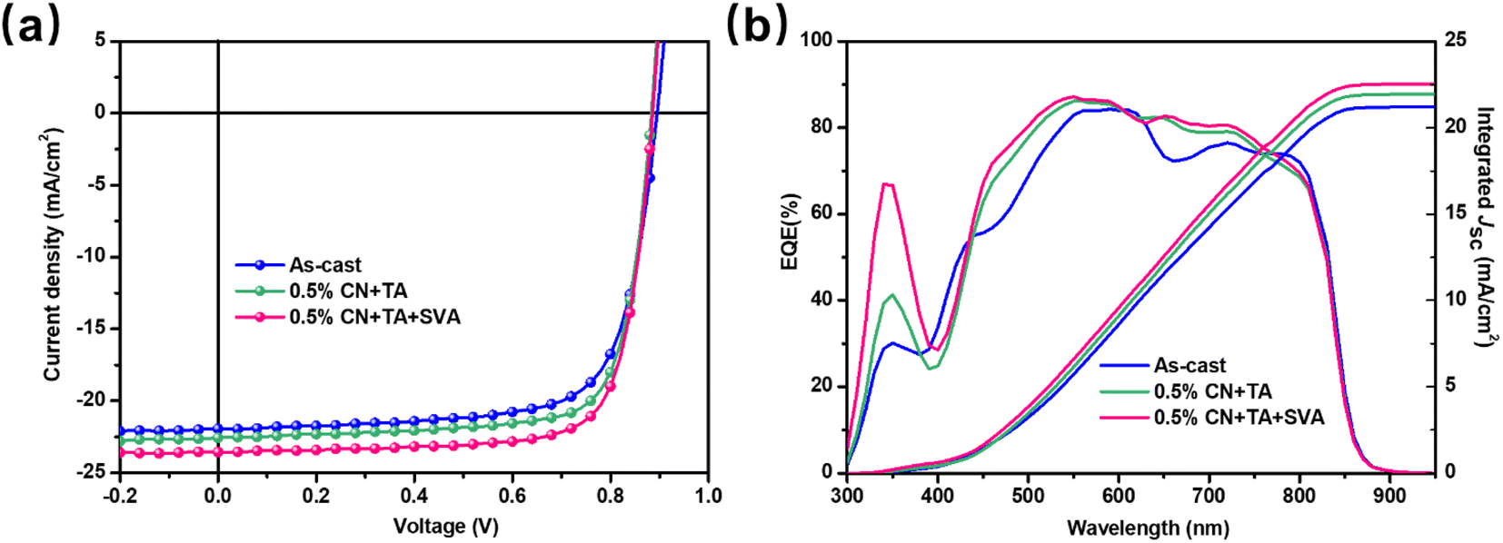
To investigate the photovoltaic performance of binary PTQ10:Y26 devices under various processing conditions, we fabricated conventional structured devices with PEDOT:PSS [poly(3,4-ethylenedioxythiophene):poly(styrene-sulfonate)], PTQ10, Y26 and PDINN (aliphatic amine-functionalized perylene-diimide) as the anode buffer layer, donor, acceptor and cathode buffer layer, respectively. Table 1 lists the photovoltaic parameters under 1 sun illumination, and Fig. 2a displays the related J–V curves for these devices. As listed in Table 1, the as-cast PTQ10:Y26 exhibits Voc, Jsc, fill factor (FF), and PCE values of 0.895 V, 21.95 mA cm−2, 0.726, and 14.29%, respectively. The device shows improved photovoltaic performance with Voc, Jsc, FF, and PCE values of 0.883 V, 22.56 mA cm−2, 0.763, and 15.23% after the treatments with 0.5% 1-chloronaphthalene (1-CN) and thermal annealing (TA). This could be ascribed to the fine-tuned BHJ phase separation induced by the additive and TA treatments. The 0.5% CN + TA + SVA-treated devices particularly with the SVA treatment for 5 min (the detailed photovoltaic performance of PTQ10:Y26 with varying SVA time is shown in Table S1†) demonstrate an outstanding PCE of over 16% with enhanced Voc of 0.886 V and Jsc of 23.57 mA cm−2. In addition, the optimized PM6:Y26 device presents a decent PCE of 15.45%. The Voc value of PM6:Y26 devices is lower than that of the PTQ10 counterparts, which may be ascribed to the lower-lying HOMO level of PTQ10, as we discussed above. Fig. S3† displays the J–V curve and external quantum efficiency (EQE) spectra as well as related integrated Jsc curve of PM6:Y26, the device with 0.5% CN + TA + SVA treatment demonstrates a significant increase in photovoltaic performance (Table S2†). This result indicates that Y26 can achieve respectable compatibility with different donors. The corresponding EQE curves for PTQ10:Y26 and integrated Jsc are also presented in Fig. 2b. The discrepancy between the integrated Jsc from EQE and the recorded Jsc from the solar simulator under one sun is less than 5%. The 0.5% CN + TA + SVA-treated devices display an increased photon response throughout a broad range from 450 nm to 800 nm relative to other untreated devices. Therefore, it is found that the integrated Jsc values of the as-cast 0.5% CN + TA-based and 0.5% CN + TA + SVA-based devices are 21.19, 21.93, and 22.52 mA cm−2, respectively.
Table 1 Photovoltaic parameters of the OSCs with different treatments under 1 sun illumination
| BHJ |
V
oc (V) |
J
sc (mA cm−2) |
FF (%) |
PCE (%) |
J
sc-EQE (mA cm−2) |
| PTQ10:Y26 |
As-cast |
0.895 |
21.95 |
72.60 |
14.29 (13.93 ± 0.25) |
21.19 |
| 0.5%CN + TA |
0.883 |
22.56 |
76.27 |
15.23 (15.00 ± 0.19) |
21.93 |
| 0.5%CN + TA + SVA |
0.886 |
23.57 |
76.73 |
16.01 (15.73 ± 0.26) |
22.52 |
| PM6:Y26 |
0.5%CN + TA + SVA |
0.848 |
23.17 |
78.64 |
15.44 (15.07 ± 0.27) |
22.17 |
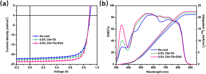 |
| | Fig. 2 (a) J–V curves and (b) EQE spectra and corresponding integrated Jsc of the PTQ10:Y26 devices with different treatments. | |
2.3 Morphology characterization
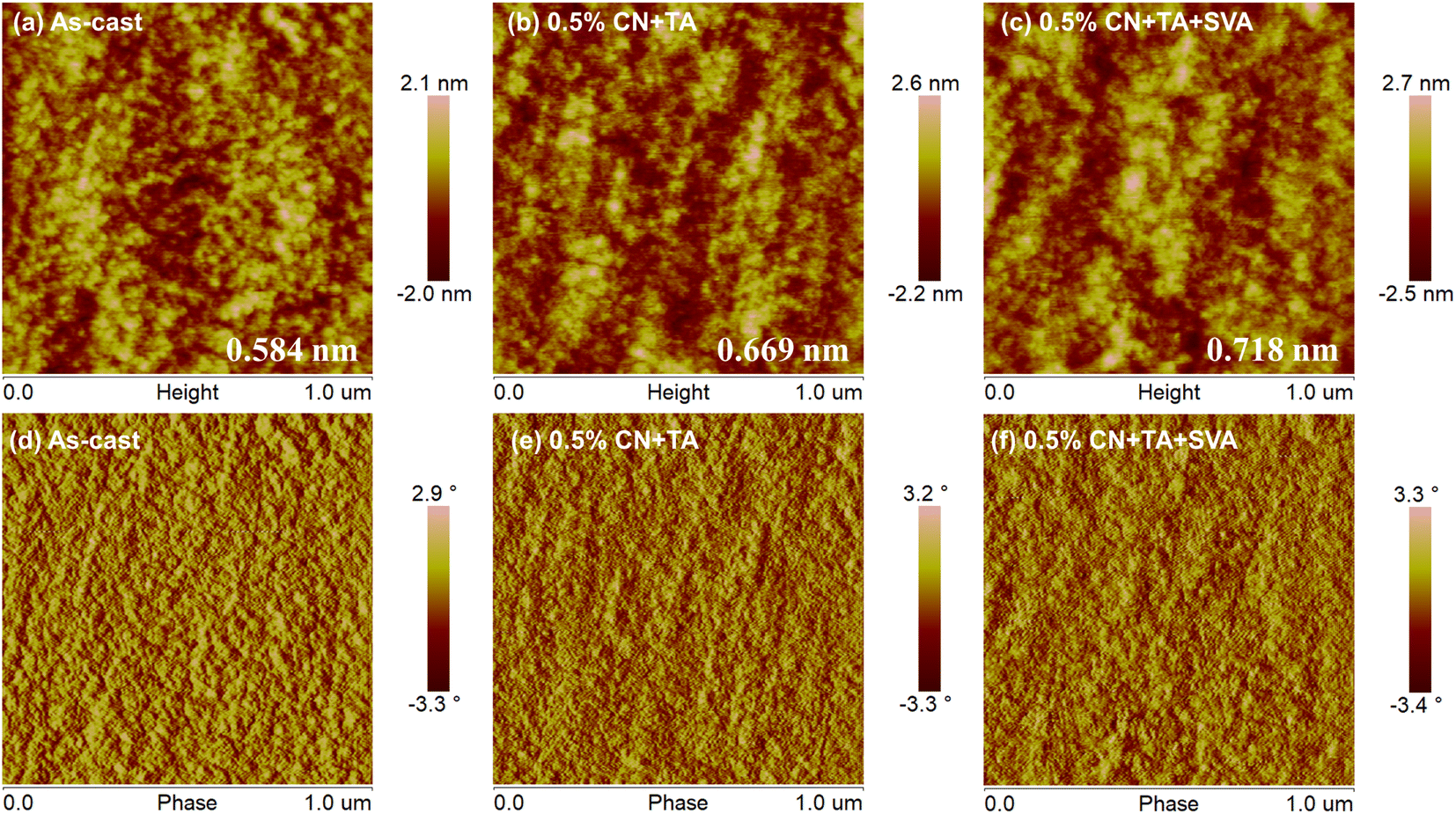
The BHJ morphology often plays a vital role in determining the device performance. Here, we used the morphological characterization techniques of transmission electron microscopy (TEM), atomic force microscopy (AFM), and grazing-incidence wide-angle X-ray scattering (GIWAXS) to illustrate the evolutions of various treatment conditions on BHJ microstructure.31,32 All the blend films have clearly interpenetrating microstructure that can be observed from both AFM (Fig. 3) and TEM images (Fig. S4†).32 The as-cast film shows a smooth surface with a low root-mean-square (RMS) roughness of 0.584 nm that may be ascribed to the good miscibility between PTQ10 and Y26. The surface energy calculation was based on the Owen model using water and glycol as testing liquids, and the values of PTQ10 and Y26 were found to be 18.239 and 15.759 mN m−1, respectively (Fig. S5†). The further Flory–Huggins interaction parameter χ between PTQ10 and Y26 was estimated to be 0.09, which confirmed the good miscibility of PTQ10 and Y26. The blend films treated with 0.5% CN and TA exhibit a rougher surface with large aggregation relative to the as-cast films, which manifests that the poor phase separation of the BHJ was responsible for the inferior photovoltaic performance of the as-cast devices. Besides, the blend film shows a obviously increased phase separation after further treatment of SVA and the RMS roughness is increased to 0.718 nm, this phenomenon may be due to 0.5% CN + TA + SVA playing a positive role in increasing the phase separation.33 However, too long SVA time will lead to the inferior performance of the devices (Table S1†), which may be ascribed to the over-large aggregation induced by CF vapor. Thus, the blend film treated with 5 min SVA time shows the highest performance due to the proper phase separation formed in the film.
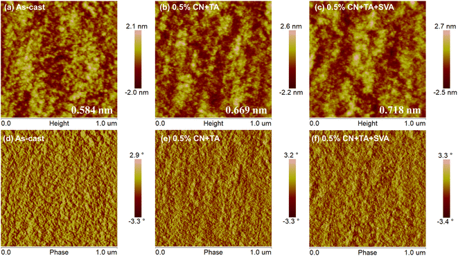 |
| | Fig. 3 (a–c) AFM height and (d–f) phase images of binary PTQ10:Y26 blend films with different treatment conditions. | |
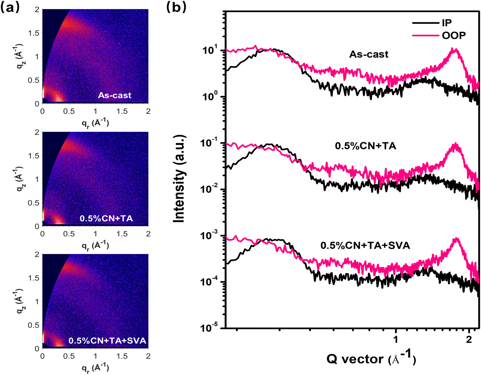
Except for the microscopic characterization, the 2D GIWAXS was carried out to understand the effects of various treatments on molecular packing and orientation. Both PTQ10 and Y26 prefer to adopt face-on orientation with the strong (010) reflection of π–π stacking peaks in the out-of-plane (OOP) direction, as shown by the scattering patterns and profiles of their pure films (Fig. S6†). The plotted 2D GIWAXS scattering patterns and corresponding profiles of the PTQ10:Y26 blend films under various conditions are shown in Fig. 4a and b. Besides, Table 2 summarizes the extracted crystallographic characteristics for all different PTQ10:Y26 films. In comparison to the as-cast blend, the (010) peak position of the blend film after 0.5% CN and TA treatments increases from 17.3 nm−1 to 17.5 nm−1. After 0.5% CN + TA + SVA treatment, the (010) peak position value increases to 17.7 nm−1, demonstrating a closer π–π stacking that is conducive to charge transport. The crystalline coherence lengths (CCLs) of these three films could be extracted from their corresponding profiles to effectively evaluate the effects of various treatments on the crystallization of blend films. In general, a better crystalline ability is associated with a higher CCL value.34 In contrast to the as-cast counterpart, the film treated with 0.5% CN and TA shows an increased CCL(010) of 2.15 nm to 2.26 nm, and the CCL(010) value of the 0.5% CN + TA + SVA-treated film could be further increased to 2.54 nm, indicating that the 0.5% CN + TA + SVA treatment plays a beneficial role in enhancing the crystallization of blend films. In addition, these three films have a strong (h00) peak of lamella stacking in the in-plane (IP) direction, and the blend film with 0.5% CN + TA + SVA treatment exhibits a higher (h00) peak position of 3.13 nm−1 than the other two films. It is suggested that the 0.5% CN + TA + SVA treatment could produce a closer lamella stacking. The PTQ10:Y26 film also shows a higher CCL(h00) of 3.99 nm after optimization by 0.5% CN and TA treatments relative to the as-cast counterpart of 3.84 nm. Finally, the highest CCL(h00) value of 4.05 nm is obtained by the blend film with the 0.5% CN + TA + SVA treatment.
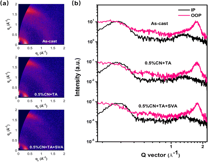 |
| | Fig. 4 (a) Two-dimensional GIWAXS scattering patterns and (b) the corresponding profiles for the binary PTQ10:Y26 blend films under different conditions. | |
Table 2 Crystallographic parameters of the PTQ10:Y26 films with different processing methods that were extracted from the GIWAXS
| Films |
IP (h00) |
OOP (010) |
| Position (Å−1) |
Distance (Å) |
CCL (nm) |
Position (Å−1) |
Distance (Å) |
CCL (nm) |
| As-cast |
0.310 |
20.27 |
3.84 |
1.73 |
3.63 |
2.15 |
| 0.5% CN + TA |
0.310 |
20.27 |
3.99 |
1.75 |
3.59 |
2.26 |
| 0.5% CN + TA + SVA |
0.313 |
20.07 |
4.05 |
1.77 |
3.55 |
2.54 |
2.4 Exciton dissociation, charge transport and recombination
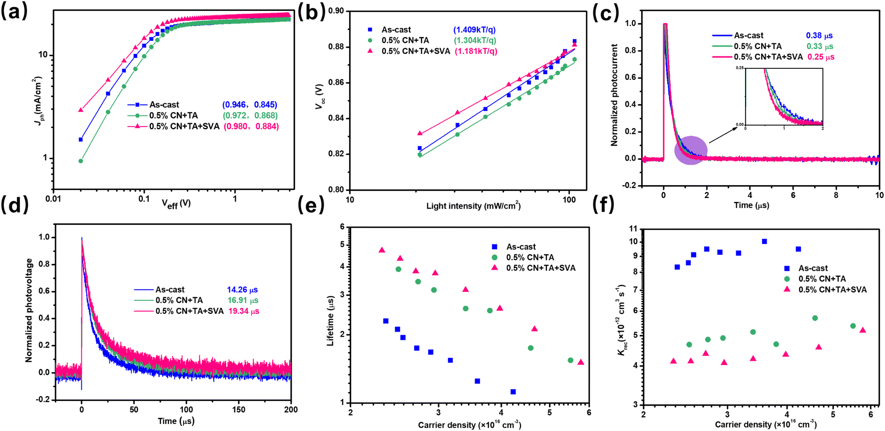
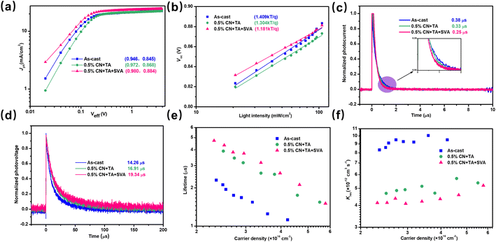
The exciton dissociation efficiency (ηdiss) was used to analyze the exciton dissociation property and can be described by the ratio between photocurrent density (Jph) and Jsat (saturated current density under high Veff).35,36 The Jph value as a function of effective voltage (Veff) characteristics of these devices can be seen in Fig. 5a. The as-cast PTQ10:Y26 device shows a low ηdiss value of 0.946, which may be ascribed to the inferior phase separation in the as-cast device. With the treatments of additive and TA, the device shows an increased ηdiss of 0.972. Finally, the 0.5% CN + TA + SVA-treated devices exhibit a further enhanced ηdiss value of 0.980, indicating the more efficient charge separation. In addition, the ratio of Jph at maximum power point (MPP) to Jsat is referred to as the charge collection efficiency (ηcoll). As a consequence, the ηcoll values of these devices were determined to be 0.845, 0.868, and 0.884, respectively. These findings suggest that post-annealing is crucial for improving Jsc and FF.
 |
| | Fig. 5 (a) Photocurrent density (Jph) as a function of effective voltage (Veff) characteristics. (b) Light intensity dependence of Voc. (c) Transient photocurrent and (d) transient photovoltage decay curves of the PTQ10:Y26 devices under different treatments. (e) Charge carrier lifetime versus charge density. (f) Bimolecular recombination rate constant Krecversus different charge densities of PTQ10:Y26 devices. | |
The hole (μh) and electron mobilities (μe) as important physical parameters to evaluate the charge transport property in OSCs could be extracted by fitting the relationship between the dark current and the bias voltage of the single-carrier devices with different BHJ processing conditions by the space charge-limited current (SCLC) method.37 As plotted in Fig. S7,† the calculated μe and μh for the as-cast device are 5.29 × 10⁻⁵ cm2 V−1 S−1 and 4.17 × 10⁻⁵ cm2 V−1 S−1, respectively. The low mobility and unbalanced μe/μh ratio of 1.27 account for the low FF and Jsc values for the as-cast device. In addition, the device with 0.5% CN and TA treatments exhibits μe and μh of 1.51 × 10⁻⁴ cm2 V−1 S−1 and 1.42 × 10⁻⁴ cm2 V−1 S−1, respectively. Finally, the 0.5% CN + TA + SVA-treated device shows the highest μe and μh of 1.80 × 10⁻⁴ cm2 V−1 S−1 and 1.76 × 10⁻⁴ cm2 V−1 S−1, respectively. The higher and more balanced μe/μh ratio of 1.02 contributes to the higher FF and Jsc values of the 0.5% CN + TA + SVA-treated devices relative to other devices.38
To carefully gain information about how various processing methods affect charge recombination in the devices, the light intensity dependence of J–V measurements was performed.39,40 Generally, the relationship between Jsc and light intensity (I) can be expressed as Jsc ∝ Iα. Bimolecular recombination means weak when the slope α is near 1.41 The dependence of Jsc on light intensity (I) of these devices is plotted in Fig. S8,† and the fitting slopes were extracted to be 0.986, 0.997, and 0.999, respectively. Compared to other devices, the as-cast devices show a more pronounced bimolecular recombination. Furthermore, the devices with 0.5% CN + TA + SVA treatment significantly reduced charge recombination. In addition, the Voc value is usually in accordance with linear dependence of ln(I) with a slope of nkT/q, where n is the ideality factor, k is the Boltzmann constant, T is the Kelvin temperature and q is the elementary charge.42 When n is far away from 1, the device is indicated to be dominated by monomolecular or trap-assisted recombination. Fig. 5b also shows the dependence of Voc on the light intensity (I) of these related devices. These fitting slopes of the as-cast, 0.5% CN + TA-treated, and 0.5% CN + TA + SVA-treated devices are 1.409 kT/q, 1.304 kT/q, and 1.181 kT/q, respectively. The as-cast devices exhibit a more severe monomolecular or trap-assisted recombination relative to other devices. After morphological optimization, the 0.5% CN + TA + SVA-treated devices show an obviously suppressed recombination.
In addition to the aforementioned characterizations, the charge recombination in the devices may be investigated by comparing the charge extraction time and charge lifetime using transient photovoltage (TPV) and transient photocurrent (TPC) technologies, respectively.43 First, the fitting charge extraction time for these curves was estimated using TPC decay dynamics (Fig. 5c). Due to the strong charge recombination inside the devices, the slowest charge extraction time of 0.38 μs was obtained for the as-cast PTQ10:Y26 devices. After treatment with the 0.5% CN and TA, the device shows a steadily reduced charge extraction time of 0.33 μs, and the subsequent 0.5% CN + TA + SVA-treated device achieves a faster value of 0.25 μs relative to other devices. As shown in Fig. 5d, the TPV curves of these devices are given and the corresponding charge lifetimes are derived by fitting the TPV curves with a single exponential decay function. The as-cast device shows the shortest charge lifetime of 14.26 μs, whereas devices treated with 0.5% CN + TA and 0.5% CN + TA + SVA have longer charge lifetimes of 16.91 μs and 19.34 μs, respectively. To get greater insights into the charge recombination information, the charge density n should be considered in addition to simply comparing the charge lifetime τ. The TPV was used to extract the charge lifetimes at different illumination intensities, and charge extraction (CE) technology was used to extract the charge density values for OSCs at different light intensities.44 The charge lifetimes as a function of charge density under different illumination intensities are plotted in Fig. 5e, the charge density n values of the as-cast, 0.5% CN + TA-treated, and 0.5% CN + TA + SVA-treated OSCs under 100% LED illumination are 4.94 × 10⁻¹⁶ cm−3, 6.68 × 10⁻¹⁶ cm−3, and 7.04 × 10⁻¹⁶ cm−3, respectively. The increased charge density may stem from the more effective exciton dissociation after morphological optimization. In addition, the bimolecular recombination rate constants (krec) of these devices could be further investigated by the equation of krec = 1/[(λ + 1)nτ], in which λ is the recombination order and could be calculated from the equation of τ = τ0n−λ.45 In general, the severity of charge recombination in the device is often correlated with a larger krec value.45 The calculated krecversus the charge density is plotted in Fig. 5f, and the as-cast devices present the highest krec values at different illumination intensities relative to the other two devices, indicating the severe bimolecular recombination inside the device. With treatments of 0.5% CN and TA, the device displays decreased krec values at different charge densities. After further treatment of SVA, the device exhibits the smallest krec value among these devices. These findings essentially show that the 0.5% CN + TA and SVA treatments substantially reduce bimolecular recombination in the device.
2.5 Thickness dependence of photovoltaic performance
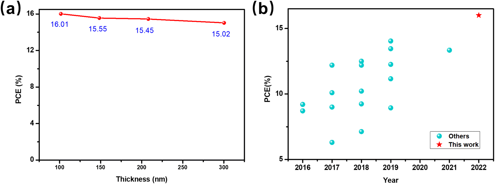
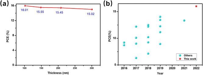
A BHJ combination with thickness insensitivity is more available for large-scale fabrication in the future. To further verify the processing potential of PTQ10:Y26, we studied the thickness dependence of its photovoltaic performance with a conventional structure. The relationship between PCE and BHJ thickness can be seen in Fig. 6a, and Table S3† provides the corresponding photovoltaic parameters. The champion device is achieved with a thickness of around 100 nm, and the efficiency is gradually decreased with the increase in thickness due to the more severe charge recombination relative to the thin film and this is also the result of competition between the thickness-dependent absorption and charge recombination. It should be noted that the device still can achieve about 15.45% efficiency when the thickness increases to about 200 nm. Further, even for the OSCs with a thickness of about 300 nm, the devices maintain high efficiencies of about 15.02%. Therefore, we make a rough comparison with other OSCs that could achieve beyond 14% PCE when the active layer thickness increased to 300 nm (Fig. S9a and Table S4†), and we found that PTQ10:Y26 could be listed as one of the best-reported thick-film OSCs. These findings indicate that the PTQ10:Y26 system exhibits favorable thickness tolerance and also has the potential for future large-scale processing.
 |
| | Fig. 6 (a) PCE of PTQ10:Y26 OSC as a function of BHJ thickness. (b) Summary of the reported OSCs based on pentacyclic acceptors. | |
2.6 i-FOM analysis
To better understand the advantage of PTQ10:Y26, we introduced the industrial figure of merit (i-FOM) to make a comprehensive comparison with other blend systems based on A–DA′D–A acceptors.22,23 As early as 2017, Min et al. proposed a first-generation i-FOM parameter to assess the commercial potential of different BHJ materials.22 This parameter could be calculated by involving three key factors, including the PCE, photostability, and synthetic complexity (SC).24 The detailed calculation of SC is shown in Section 1.2, ESI.† We only consider the PCE and SC since the photostability measurement is not uniform under various testing conditions. As a result, this parameter might be expressed more simply as i-FOM = PCE/SC.46 Moreover, the SC of the overall BHJ should take the ratio of donor and acceptor into account when fabricating the BHJ. In addition, the average SC (ASC) could be calculated according to the equation of SCD:A = (SCD × wD + SCA × wA)/(wD + wA).
Some classic BHJ systems based on A–DA′D–A acceptors were selected as listed in Table 3, and the SC of donor and acceptor materials used in this table is summarized in Table S6.† The PTQ10:Y6 combination shows great cost potential with a high average FOM (AFOM) of 0.255 and a high PCE of 16.21%. It should be noted that after continuous optimization, the highest PCE value of a certain BHJ system gradually increases, resulting in an unfixed AFOM value. In addition, developing the easily synthesized polythiophene (PT) donor is another direction to lower the cost of OSCs. A series of PT-based donors were reported and declared a lot of advantages such as easy synthesis and high efficiency. As a consequence, a few high-performance PT-based BHJ combinations are discussed. One of the highest PCEs for the PT-based device reported so far was achieved by the P5TCN-F25:Y6 combination, which demonstrated a high efficiency of 16.6%. The SC of P5TCN-F25 is significantly reduced relative to PM6 and D18.47 However, the high SC of the acceptor Y6 gives rise to a slightly low AFOM of the P5TCN-F25:Y6. Hence, some efforts are made to decrease the acceptor cost. As mentioned above, the pentacyclic A–DA′D–A acceptor Y26 was synthesized with reduced synthesis steps and increased yields. The PM6:Y26 combination shows a low AFOM of 0.17 because of the high SC of PM6 and a low PCE of 13.34%. By blending with the low-cost donor PTQ10, the AFOM of PTQ10:Y26 could be calculated to be 0.309 (Fig. S9b†). Moreover, the high PCE of 16.01% for PTQ10:Y26 OSCs is one of the highest PCEs for OSCs based on pentacyclic acceptors until now (Fig. 6b, Table S5†).
Table 3 Summary of some typical systems based on A–DA′D–A acceptors
| BHJ |
D:A ratio |
SCD |
SCA |
ASC |
PCE |
AFOM |
Year |
Ref. |
| PM6:Y6 |
1:1.2 |
92.37 |
88.09 |
90.03 |
15.7 |
0.174 |
2019 |
10
|
| PTQ10:Y6 |
1:1.2 |
34.21 |
88.09 |
63.60 |
16.21 |
0.255 |
2019 |
27
|
| PM7:Y6 |
1:1.2 |
70.925 |
88.09 |
80.29 |
17.04 |
0.212 |
2020 |
48
|
| D18:Y6 |
1:1.6 |
94.765 |
88.09 |
90.66 |
18.22 |
0.201 |
2020 |
47
|
| P4T2F-HD:Y6-BO |
1:1.2 |
52.52 |
82.595 |
68.92 |
13.65 |
0.198 |
2021 |
46
|
| PM6:Y26 |
1:1.2 |
92.37 |
66.53 |
78.28 |
13.34 |
0.170 |
2021 |
29
|
| P3HT:ZY-4Cl |
1:1 |
9.545 |
71.28 |
40.41 |
10.7 |
0.265 |
2022 |
49
|
| P5TCN-F25:Y6 |
1:1.2 |
61.745 |
88.09 |
76.12 |
16.6 |
0.218 |
2022 |
50
|
| PTQ10:Y26 |
1:1.2 |
34.21 |
66.53 |
51.84 |
16.01 |
0.309 |
— |
This work |
3. Conclusion
In summary, we have successfully demonstrated high-performance and low-cost PTQ10:Y26 OSCs by optimization. The solvent vapor annealing could produce an increased phase separation as well as improve the molecular packing and orientation, which is beneficial for achieving higher Jsc and FF. As a result, the 0.5% CN + TA + SVA-treated device shows a high PCE of 16.01%, which is comparable to the first reported efficiency of OSCs based on heptacyclic acceptors like Y6 and Y11. Besides, a high PCE of 15.02% is even achieved with a 300 nm-thick BHJ film due to the good thickness tolerance of the PTQ10:Y26 blend. On the other hand, the i-FOM parameter was used to evaluate the industrialization potential of PTQ10:Y26, and we compared it with other classic systems based on A–DA′D–A acceptors and found that a high AFOM value of about 0.309 was obtained for the PTQ10:Y26 system. These results demonstrate that PTQ10:Y26 could be one of the excellent candidates for large-scale processing.
4. Experimental section
4.1 Materials
PEDOT:PSS (4083) was purchased from Xi'an Polymer Light Technology Corp. Acceptor Y26 was synthesized according to the procedure reported in the literature.29 PM6 was purchased from Solarmer Materials Inc. PTQ10 was purchased from 1-Material, Inc. The PDINN was purchased from Nanjing Zhiyan Technology Co., Ltd.
4.2 Device fabrication
The solar cell devices were fabricated with a conventional structure of Glass/ITO/PEDOT:PSS(40 nm)/Active layer/PDINN (5 nm)/Ag. Deionized water and isopropyl alcohol were used to wash pre-patterned ITO-coated glass substrates for 15 minutes each in an ultrasonic bath. All ITO substrates are treated in the UV ozone cleaning system for 25 minutes after blow-drying with high-purity nitrogen. A thin film of PEDOT:PSS was then spin-coated at 6000 rpm for 30 s on a previously cleaned ITO-coated glass and dried at 150 °C for 15 minutes in ambient air. After that, a mixed (CF:CN, 99.5%:0.5%, v/v) solution of BHJ (D:A = 1:1.2, w/w) with a final concentration of 16 mg mL−1 was spin-coated onto the PEDOT:PSS layers in a glovebox. Thermal annealing at 100 °C for 10 minutes was used to treat the BHJ films. The BHJ films were then put in a Petri dish with a CF atmosphere for 5 minutes. At a rate of 3000 rpm for 30 s, a PDINN layer was deposited on the top of the active layer. Finally, at a vacuum of 1.5 × 10⁻⁴ mbar, the top Ag electrode with a thickness of 100 nm was thermally evaporated onto the cathode buffer layer through a mask. The thickness of the optimal active layer measured using a Bruker Dektak XT stylus profilometer was about 100 nm.
4.3 Device measurement and characterization
The detailed device measurement and related characterization in this work are depicted in ESI 1.1.†
Author contributions
Yingping Zou and Xiang Xu conceived the idea and designed the experiment. Xiang Xu performed the device fabrication and characterization, analyzed the data and wrote the original draft. Qingya Wei and Jiage Song synthesized the Y26. Jianhua Jing performed the TPV and CE technologies under different illumination intensities. Yanwei Chen carried out the TPC and TPV measurements. Xinhui Lu performed the GIWAXS characterization. Yingping Zou directed this research project. All the authors participated in the revision of the manuscript.
Conflicts of interest
The authors declare there are no conflicts of interest.
Acknowledgements
This work was supported by National Natural Science Foundation of China (52125306, 21875286).
References
- M. A. Green, Prog. Photovoltaics, 2001, 9, 123–135 Search PubMed.
- J. Hou, O. Inganäs, R. H. Friend and F. Gao, Nat. Mater., 2018, 17, 119 CrossRef PubMed.
- L. Feng, J. Yuan, Z. Zhang, H. Peng, Z.-G. Zhang, S. Xu, Y. Liu, Y. Li and Y. Zou, ACS Appl. Mater. Interfaces, 2017, 9, 31985–31992 CrossRef PubMed.
- J. Zhang, H. S. Tan, X. Guo, A. Facchetti and H. Yan, Nat. Energy, 2018, 3, 720–731 CrossRef.
- Y. Lin, J. Wang, Z.-G. Zhang, H. Bai, Y. Li, D. Zhu and X. Zhan, Adv. Mater., 2015, 27, 1170–1174 CrossRef CAS PubMed.
- J. Yuan, Y. Zhang, L. Zhou, G. Zhang, H.-L. Yip, T.-K. Lau, X. Lu, C. Zhu, H. Peng and P. A. Johnson, Joule, 2019, 3, 1140–1151 CrossRef CAS.
- X. Xu, J. Xiao, G. Zhang, L. Wei, X. Jiao, H.-L. Yip and Y. Cao, Sci. Bull., 2020, 65, 208–216 CrossRef CAS.
- Y. Li, X. Huang, K. Ding, H. K. Sheriff, L. Ye, H. Liu, C.-Z. Li, H. Ade and S. R. Forrest, Nat. Commun., 2021, 12, 1–9 CrossRef PubMed.
- Y. Han, H. Dong, W. Pan, B. Liu, X. Chen, R. Huang, Z. Li, F. Li, Q. Luo and J. Zhang, ACS Appl. Mater. Interfaces, 2021, 13, 17869–17881 CrossRef CAS PubMed.
- X. Xu, D. Li, J. Yuan, Y. Zhou and Y. Zou, EnergyChem, 2021, 3, 100046 CrossRef CAS.
- C. Li, J. Zhou, J. Song, J. Xu, H. Zhang, X. Zhang, J. Guo, L. Zhu, D. Wei, G. Han, J. Min, Y. Zhang, Z. Xie, Y. Yi, H. Yan, F. Gao, F. Liu and Y. Sun, Nat. Energy, 2021, 6, 605–613 CrossRef.
- Y. Cui, H. Yao, J. Zhang, K. Xian, T. Zhang, L. Hong, Y. Wang, Y. Xu, K. Ma, C. An, C. He, Z. Wei, F. Gao and J. Hou, Adv. Mater., 2020, 32, 1908205 CrossRef PubMed.
- X. Xu, Y. Qi, X. Luo, X. Xia, X. Lu, J. Yuan, Y. Zhou and Y. Zou, Fundam. Res., 2022 DOI:10.1016/j.fmre.2022.01.025.
- J. Yuan and Y. Zou, Org. Electron., 2022, 106436 CrossRef.
- Q. Wei, W. Liu, M. Leclerc, J. Yuan, H. Chen and Y. Zou, Sci. China: Chem., 2020, 63, 1352 CrossRef.
- G. Zhang, X.-K. Chen, J. Xiao, P. C. Chow, M. Ren, G. Kupgan, X. Jiao, C. C. Chan, X. Du and R. Xia, Nat. Commun., 2020, 11, 1–10 CrossRef PubMed.
- P. Bi, S. Zhang, Z. Chen, Y. Xu, Y. Cui, T. Zhang, J. Ren, J. Qin, L. Hong, X. Hao and J. Hou, Joule, 2021, 5, 2408–2419 CrossRef CAS.
- J. Yuan, C. Zhang, H. Chen, C. Zhu, S. H. Cheung, B. Qiu, F. Cai, Q. Wei, W. Liu and H. Yin, Sci. China: Chem., 2020, 63, 1159–1168 CrossRef CAS.
- J. Yuan, H. Zhang, R. Zhang, Y. Wang, J. Hou, M. Leclerc, X. Zhan, F. Huang, F. Gao, Y. Zou and Y. Li, Chem, 2020, 6, 2147–2161 CAS.
- X. Xu, C. Sun, J. Jing, T. Niu, X. Wu, K. Zhang, F. Huang, Q. Xu, J. Yuan, X. Lu, Y. Zhou and Y. Zou, ACS Appl. Mater. Interfaces, 2022, 14, 36582–36591 CrossRef CAS PubMed.
- Z. Zheng, J. Wang, P. Bi, J. Ren, Y. Wang, Y. Yang, X. Liu, S. Zhang and J. Hou, Joule, 2022, 6, 171–184 CrossRef CAS.
- J. Min, Y. N. Luponosov, C. Cui, B. Kan, H. Chen, X. Wan, Y. Chen, S. A. Ponomarenko, Y. Li and C. J. Brabec, Adv. Energy Mater., 2017, 7, 1700465 CrossRef.
- W. Yang, W. Wang, Y. Wang, R. Sun, J. Guo, H. Li, M. Shi, J. Guo, Y. Wu, T. Wang, G. Lu, C. J. Brabec, Y. Li and J. Min, Joule, 2021, 5, 1209–1230 CrossRef.
- R. Po, G. Bianchi, C. Carbonera and A. Pellegrino, Macromolecules, 2015, 48, 453–461 CrossRef CAS.
- C. Sun, F. Pan, H. Bin, J. Zhang, L. Xue, B. Qiu, Z. Wei, Z.-G. Zhang and Y. Li, Nat. Commun., 2018, 9, 1–10 CrossRef PubMed.
- Y. Wu, Y. Zheng, H. Yang, C. Sun, Y. Dong, C. Cui, H. Yan and Y. Li, Sci. China: Chem., 2020, 63, 265–271 CrossRef CAS.
- C. Sun, F. Pan, S. Chen, R. Wang, R. Sun, Z. Shang, B. Qiu, J. Min, M. Lv, L. Meng, C. Zhang, M. Xiao, C. Yang and Y. Li, Adv. Mater., 2019, 31, 1905480 CrossRef CAS PubMed.
- Y. Zhou, M. Li, H. Lu, H. Jin, X. Wang, Y. Zhang, S. Shen, Z. Ma, J. Song and Z. Bo, Adv. Funct. Mater., 2021, 31, 2101742 CrossRef CAS.
- J. Song, F. Cai, C. Zhu, H. Chen, Q. Wei, D. Li, C. Zhang, R. Zhang, J. Yuan, H. Peng, S. K. So and Y. Zou, Sol. RRL, 2021, 5, 2100281 CrossRef CAS.
- X. Li, F. Pan, C. Sun, M. Zhang, Z. Wang, J. Du, J. Wang, M. Xiao, L. Xue, Z.-G. Zhang, C. Zhang, F. Liu and Y. Li, Nat. Commun., 2019, 10, 519 CrossRef CAS PubMed.
- P. Müller-Buschbaum, Adv. Mater., 2014, 26, 7692–7709 CrossRef PubMed.
- F. Zhao, C. Wang and X. Zhan, Adv. Energy Mater., 2018, 8, 1703147 CrossRef.
- K. Sun, Z. Xiao, E. Hanssen, M. F. G. Klein, H. H. Dam, M. Pfaff, D. Gerthsen, W. W. H. Wong and D. J. Jones, J. Mater. Chem. A, 2014, 2, 9048–9054 RSC.
- D.-M. Smilgies, J. Appl. Crystallogr., 2009, 42, 1030–1034 CrossRef.
- V. D. Mihailetchi, L. J. A. Koster, J. C. Hummelen and P. W. M. Blom, Phys. Rev. Lett., 2004, 93, 216601 CrossRef CAS PubMed.
- P. W. M. Blom, V. D. Mihailetchi, L. J. A. Koster and D. E. Markov, Adv. Mater., 2007, 19, 1551–1566 CrossRef CAS.
- P. Murgatroyd, J. Phys. D: Appl. Phys., 1970, 3, 151 CrossRef.
- W. Tress, A. Petrich, M. Hummert, M. Hein, K. Leo and M. Riede, Appl. Phys. Lett., 2011, 98, 23 CrossRef.
- L. J. A. Koster, V. Mihailetchi, H. Xie and P. W. Blom, Appl. Phys. Lett., 2005, 87, 203502 CrossRef.
- V. Shrotriya, G. Li, Y. Yao, T. Moriarty, K. Emery and Y. Yang, Adv. Funct. Mater., 2006, 16, 2016–2023 CrossRef CAS.
- L. J. A. Koster, M. Kemerink, M. M. Wienk, K. Maturová and R. A. Janssen, Adv. Mater., 2011, 23, 1670–1674 CrossRef CAS PubMed.
- L. J. A. Koster, V. D. Mihailetchi, R. Ramaker and P. W. Blom, Appl. Phys. Lett., 2005, 86, 123509 CrossRef.
- Z. Li, F. Gao, N. C. Greenham and C. R. McNeill, Adv. Funct. Mater., 2011, 21, 1419–1431 CrossRef CAS.
- C. G. Shuttle, A. Maurano, R. Hamilton, B. O'Regan, J. C. d. Mello and J. R. Durrant, Appl. Phys. Lett., 2008, 93, 183501 CrossRef.
- C. G. Shuttle, B. O'Regan, A. M. Ballantyne, J. Nelson, D. D. Bradley and J. R. Durrant, Phys. Rev. B, 2008, 78, 113201 CrossRef.
- J. Xiao, X. e. Jia, C. Duan, F. Huang, H.-L. Yip and Y. Cao, Adv. Mater., 2021, 33, 2008158 CrossRef PubMed.
- Q. Liu, Y. Jiang, K. Jin, J. Qin, J. Xu, W. Li, J. Xiong, J. Liu, Z. Xiao, K. Sun, S. Yang, X. Zhang and L. Ding, Sci. Bull., 2020, 65, 272–275 CrossRef.
- R. Ma, T. Liu, Z. Luo, Q. Guo, Y. Xiao, Y. Chen, X. Li, S. Luo, X. Lu and M. Zhang, Sci. China: Chem., 2020, 63, 325–330 CrossRef.
- K. Xian, Y. Liu, J. Liu, J. Yu, Y. Xing, Z. Peng, K. Zhou, M. Gao, W. Zhao and G. Lu, J. Mater. Chem. A, 2022, 10, 3418–3429 RSC.
- X. Yuan, Y. Zhao, D. Xie, L. Pan, X. Liu, C. Duan, F. Huang and Y. Cao, Joule, 2022, 6, 647–661 CrossRef CAS.
|
| This journal is © The Royal Society of Chemistry 2022 |
Click here to see how this site uses Cookies. View our privacy policy here. 
 b,
Xinhui
Lu
c,
Yonghua
Zhou
b,
Xinhui
Lu
c,
Yonghua
Zhou