
Organic–inorganic halide perovskite based solar cells – revolutionary progress in photovoltaics
Xiangye
Liu
a,
Wei
Zhao
b,
Houlei
Cui
b,
Yi'an
Xie
b,
Yaoming
Wang
*b,
Tao
Xu
*c and
Fuqiang
Huang
*a
aBeijing National Laboratory for Molecular Sciences and State Key Laboratory of Rare Earth Materials Chemistry and Applications, College of Chemistry, Peking University, Beijing 100871, P.R. China. E-mail: huangfq@pku.edu.cn; Fax: (+86)10-62758225
bCAS Key Laboratory of Materials for Energy Conversion, Shanghai Institute of Ceramics, Chinese Academy of Sciences, Shanghai 200050, P.R. China. E-mail: wangyaoming@mail.sic.ac.cn
cDepartment of Chemistry and Biochemistry, Northern Illinois University, DeKalb, Illinois 60115, USA. E-mail: txu@niu.edu
First published on 30th January 2015
Abstract
Photovoltaic technology has been presented with a great opportunity for development, owing to the recent and unprecedented rapid development of a new-type of solar cell based on organic–inorganic halide perovskites. Their power conversion efficiency (η) has surpassed 19% since the first perovskite-based solar cell (η = 3.8%) was reported in 2009. Moreover, this performance seems to be still far from fully optimized because of its versatile fabrication techniques and device configurations. In this review, the history of perovskites for photovoltaic applications and the landmark achievements to date are briefly outlined. Focusing on these new halide perovskite solar absorbers, the crystal structure, electronic structure, and intrinsic physical properties are systematically described, in an attempt to unravel the origins of superior solar cell performance. To meet the requirements of high-efficiency photovoltaics, the unique solar perovskite absorbers and electron and hole transport materials are discussed, as well as some unanswered questions and challenges facing their further development and commercialization.
 Xiangye Liu | Xiangye Liu is currently a 4th year PhD student at the College of Chemistry and Molecular Engineering, Peking University, under the guidance of Prof. Fuqiang Huang. He received his BS degree in chemistry from Hebei University, China in 2011. His thesis research focuses on the design and synthesis of nanomaterials for solar energy applications. |
 Yaoming Wang | Prof. Yaoming Wang received his PhD in chemistry from Shanghai Institute of Ceramics, Chinese Academy of Sciences in 2009. He became associate professor at Shanghai Institute of Ceramics, Chinese Academy of Sciences in 2012. He is an expert on CIGS and CdTe thin film solar cells. His current research interests are new Cu-based solar materials and new photovoltaic devices including perovskite-type solar cells. |
 Tao Xu | Prof. Tao Xu received his PhD in Chemistry from The University of Alabama in 2003. He worked as a post-doc at Texas A&M University and Argonne National Laboratory during 2003–2006. He became an assistant professor at the Department of Chemistry and Biochemistry, Northern Illinois University in 2006 and was promoted to associate professor in 2011. His current research interests are nanoscale materials for energy and environmental science applications. |
 Fuqiang Huang | Prof. Fuqiang Huang received his PhD in chemistry from Beijing Normal University in 1996. He worked as a researcher at University of Michigan, Northwest University, Osram Sylvania Inc. and University of Pennsylvania during 1996–2003. He became a professor at Shanghai Institute of Ceramics, Chinese Academy of Sciences in 2004 and joined as a full professor at College of Chemistry and Molecular Engineering, Peking University in 2010. His current research interests are energy materials and photovoltaic applications. |
1 Introduction
Sunlight, the most abundant and clean renewable energy source, is definitely capable of sustaining our economic growth. Since the photovoltaic (PV) effect was discovered by Edmond Becquerel in 1839, researchers and engineers have been interested in the idea of developing efficient and cost-effective materials and PV cells to directly convert solar photons into electric power. Multicrystalline Si solar cells, known as first generation PV cells, are currently dominant in the PV market with photoelectric conversion efficiencies (PCE) close to 20% (for 1 cm2 cells). However, the high production cost unavoidably limits their large-scale civil application. Second generation PV cells based on thin-film devices achieved relatively significant progress in terms of diminishing manufacturing cost. Among various thin-film semiconductor compounds, copper indium gallium diselenide (CIGS) has been the star material for its high PCE (21.7% for 0.5 cm2 cells), comparable to mono-crystalline Si, but with a remarkably lower cost, lower efficiency-decay under long irradiation times and excellent weak light performance. However, the widely used vacuum manufacturing techniques prevent it from achieving its full success in large-scale production.In the last decade, the “new concept type” PV cells based on nanotechnologies and inexpensive solution processes have made great strides. Dye-sensitized solar cells (DSSCs) are the front runners in this new PV technology due to their cost-effectiveness, ease of fabrication and high efficiencies. Furthermore, the configuration of DSSCs relaxes the material quality requirements necessary with Si solar cells, owing to the separate transport of photo-generated electrons and holes in different materials. Mesoscopic DSSCs based on nanocrystalline TiO2 sensitized by Ru(bpy)2+ were first introduced by Grätzel in 1985 and then a record PCE of 12%1 was achieved by his team in 1991 that spurred much scientific effort into these types of devices. Recently, a PCE exceeding 13% was reported using a porphyrin photosensitizer and cobalt(II/III)-based redox electrolyte.2 However, organic sensitizers have inevitably been limited by their low light-harvesting ability and poor lifetime stability. In order to replace conventional organic-type sensitizers, inorganic semiconductor quantum dots (QDs) such as metal-chalcogenides (CdS, PbS, Sb2S3, etc.) and III–V group semiconductors were intensively investigated. Their numerous outstanding properties, including tunable energy band gaps, large optical absorption coefficients and carrier multiplication, unfortunately, have not endowed the PV cells with high performance. Significant losses of photo-generated carriers are mainly caused by the electronic trap states presented in the semiconductor nanocrystals owing to their high surface area to volume ratios.3
Recently, the emergence and development of organic–inorganic halide perovskite-based solar cells (PSCs) have kindled tremendous research enthusiasm, owing to their perfect combination of high efficiency and low cost solution-based fabrication process. Since the first report of a CH3NH3PbX3 (X = Br, I) sensitized liquid junction cell in 2009,4 the PCEs of the PSCs have rocketed to 19.3%.5 This explosion in progress is rarely seen in other historical solution-processed solar cell technologies. Therefore, the halide perovskite's excellent properties of light harvesting and charge transfer have undoubtedly opened a new era for PV technology.
In this review, we will first describe the crystal structure and the intrinsic physical and electronic properties of this class of halide perovskites, in an attempt to unravel the origins of their superior solar cell performance. Then we focus on the progress in PSCs, referring to the device configuration, working principles and fabrication technology, followed by a summary of the different perovskite materials, the electron transport materials (ETMs) and the hole transport materials (HTMs). Finally, we end with a brief summary and outlook on perovskite-based PV cells.
2 Intrinsic properties of halide perovskites
2.1 Crystal structure
Perovskite refers to a type of oxide mineral of calcium titanate, with the chemical formula CaTiO3. This mineral was discovered in the Ural Mountains of Russia by Gustav Rose in 1839 and is named after the Russian mineralogist Lev Perovskite.6 Now the word “perovskite” is chosen to describe any compound crystallized with the same structure as CaTiO3. A pure perovskite compound can be represented by the general chemical formula AMX3, where both A and M are cations and X is an anion. In an ideal perovskite structure, M is octahedrally coordinated with X forming a building block of MX6, and MX6 octahedra connect with each other sharing every corner to give a three-dimensional network, shown in Fig. 1. A cations fill in the hollows formed by every eight adjacent MX6 octahedra and thus balance the charge of the entire network (Fig. 1b). Large numbers of inorganic perovskite oxides and halides have been extensively studied owing to their versatile properties in optics,7 magnetics,8 electronics9 and electrochemistry.10 | ||
| Fig. 1 Crystal structure of cubic perovskite of general formula AMX3. | ||
For the organic–inorganic halide perovskites discussed here, A cations are organic ammonium ions, and M cations are divalent metal ions such as Cu2+, Mn2+, Pd2+, Sn2+, Eu2+, etc., while the X anions are halides (Cl−, Br−, I−). These belong to a large family which have attracted extensive scientific interest since the 1970s for their structural versatility and magnetic, optical, and electric properties.11 The organic–inorganic halide perovskite systems with metal ions Sn2+ or Pb2+ in the M site generated initial interest in the early 1990s, with researchers focusing on their semiconductor-metal transition properties,12,13 high carrier mobility for thin film transistors14 and strong excitonic features for light-emitting diodes.15 Not until 20094 did the class of compounds MAMX3 (MA = CH3NH3; M = Pb, Sn; X = Cl−, Br−, I−) reignite scientific excitement as new visible-light absorbers and excellent charge transport materials for PV cells, which led to a renaissance of this organic–inorganic perovskite material. In these compounds, the [MX6]4− octahedra can form chained16–18 or layered or three dimensional (3D) networks depending on the characteristics of the organic ammonium cations at the A site.
The general formula for a typical <100> oriented layered organic–inorganic halide perovskite can be written as (R-NH3)2MAn−1MnX3n+1, where R-NH3+ is an alkylammonium or phenethylammonium species.11,12 The <100> oriented inorganic perovskite sheet alternates with a bilayer of R-NH3+ organic cations and n refers to the number of perovskite sheets. The NH3+ heads of the organic cations form hydrogen/ionic bonds with the halogens in the perovskite sheets and the hydrocarbon tails R extend into the space between the perovskite sheets, forming a van der Waals gap. As n → ∞, MAMX3 with a 3D structure is encountered. This is shown in Fig. 2.
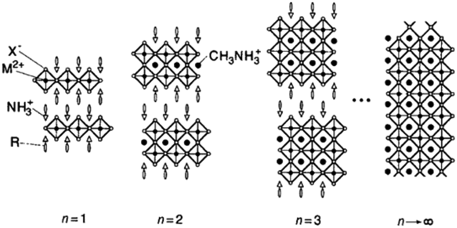 | ||
| Fig. 2 Schematic illustration of the <100> oriented hybrid perovskite family with the general formula (R-NH3)2MAn−1MnX3n+1 (reproduced with permission11). | ||
As with the 3D perovskites AMX3, their crystallographic structure formability can be empirically estimated by the Goldschmidt tolerance factor t and an octahedral factor μ. t = (tA + tX)/[21/2(tM + tX)] and μ = tM/tX, where tA, tM, and tX are the effective ionic radii for the ion at the A, M, and X sites, respectively. A study of the formability of alkali metal halide perovskites indicated that the ideal cubic structure was stabilized provided the t factor ranges between 0.813 and 1.107 and the μ factor ranges from 0.442 to 0.895.19 Lower t values give a lower symmetric tetragonal or orthorhombic structure. Taking MAPbX3 as an example, the radii of MA+ = 180 pm, Pb2+ = 119 pm, Cl− = 181 pm, Br− = 196 pm, and I− = 220 pm, thus the t factors for MAPbX3 are calculated to be 0.85, 0.84, and 0.83, and the μ factors are 0.66, 0.61, and 0.54, for X = Cl, Br, and I, respectively. Thus, methylammonium lead halide perovskites are expected to have a cubic structure. Despite these constraints, phase transitions of MAPbX3 occur with variation of temperature. The temperature-dependent structures of MAPbX3 are summarized in Table 1. At low temperature, MAPbX3 forms in an orthorhombic phase (space group: Pnma), which successively transforms into a tetragonal (space group: I4/m) and cubic structure (space group: Pm![[3 with combining macron]](https://www.rsc.org/images/entities/char_0033_0304.gif) m) with increasing temperature. The position of the MA+ can only be fixed in the orthorhombic phase at low temperature, because it is found to be disordered in the higher symmetric structures. For example, a cubic structure requires eight identical positions for the cation in such a way that the tetrahedral coordinated C and N atoms show random distribution inside the eight tetrahedrons of the cuboctahedron around the normal A position (1/2, 1/2, 1/2).20 A more recent work studied the structure of MAPbI3 in detail with variable temperature powder X-ray diffraction.21 The results showed that MAPbI3 has a tetragonal structure at room temperature, which transforms to a cubic phase when heated to 57.3 °C and to an orthorhombic structure when cooled to about 100 K. From cubic to tetragonal to orthorhombic structures, there is an continuous tilting of the [PbI6] octahedra around the c axes.20,21 It is worth noting that the structures of perovskites are not simply dependent on temperature. For example, high energy X-ray diffraction data showed that 70% of the MAPbI3 within mesoporous TiO2 formed in a highly disordered phase with a structural coherence length of only ∼1.4 nm, although the MAPbI3 film was annealed at 100 °C.22 Fully characterizing and controlling the crystallinity of the perovskite layer is important for its improved photovoltaic performance.
m) with increasing temperature. The position of the MA+ can only be fixed in the orthorhombic phase at low temperature, because it is found to be disordered in the higher symmetric structures. For example, a cubic structure requires eight identical positions for the cation in such a way that the tetrahedral coordinated C and N atoms show random distribution inside the eight tetrahedrons of the cuboctahedron around the normal A position (1/2, 1/2, 1/2).20 A more recent work studied the structure of MAPbI3 in detail with variable temperature powder X-ray diffraction.21 The results showed that MAPbI3 has a tetragonal structure at room temperature, which transforms to a cubic phase when heated to 57.3 °C and to an orthorhombic structure when cooled to about 100 K. From cubic to tetragonal to orthorhombic structures, there is an continuous tilting of the [PbI6] octahedra around the c axes.20,21 It is worth noting that the structures of perovskites are not simply dependent on temperature. For example, high energy X-ray diffraction data showed that 70% of the MAPbI3 within mesoporous TiO2 formed in a highly disordered phase with a structural coherence length of only ∼1.4 nm, although the MAPbI3 film was annealed at 100 °C.22 Fully characterizing and controlling the crystallinity of the perovskite layer is important for its improved photovoltaic performance.
| Phase | Temperature (K) | Crystal system | Space group | Lattice (pm) | Volume (106 pm3) |
|---|---|---|---|---|---|
| MAPbCl3 | |||||
| α | >178.8 | Cubic | Pm3m | a = 567.5 | 182.8 |
| β | 172.9–178.8 | Tetragonal | P4/mmm | a = 565.6 c = 563.0 | 180.1 |
| γ | <172.9 | Orthorhombic | P2221 | a = 567.3 b = 562.8 c = 1118.2 | 357.0 |
| MAPbBr3 | |||||
| α | >236.9 | Cubic | Pm3m | a = 590.1(1) | 206.3 (260 K) |
| β | 155.1–236.9 | Tetragonal | P4/mcm | a = 832.2(2) c = 1183.2(7) | 819.4 |
| γ | 146.9–155.1 | Tetragonal | P4/mmm | a = 589.4(2) c = 586.1(2) | |
| δ | <144.5 | Orthorhombic | Pna21 | a = 797.9(1) b = 858.0(2) c = 1184.9(2) | 811.1 |
| MAPbI3 | |||||
| α | >327.4 | Cubic | Pm3m | a = 632.85(4) | 253.5 |
| β | 162.2–327.4 | Tetragonal | P4/mcm | a = 885.5(6) c = 1265.9(8) | 992.6 |
| γ | <162.2 | Orthorhombic | Pna21 | a = 886.1(2) b = 858.1(2) c = 1262.0(3) | 959.5 |
2.2 Electronic structure
Earlier research has calculated the Pb and Sn based halide perovskites (3D and low-dimensional) using the formalism of the extended Hückel theory as well as an ab initio Hartree–Fock LCAO approach.23 The calculation result overestimated the band gap energy of MAPbX3. First principles density functional theory (DFT) band calculations on the room temperature cubic phase MAPbX3 reveal that its electronic structure is dominated by the characteristics of the Pb–X bonds24,25: the top of the valence band (VB) mainly consists of the σ-antibonding states of Pb 6s and X p orbitals, and the bottom of the conduction band (CB) is primarily composed of the σ-antibonding states of Pb 6p and X s orbitals. In spite of these hybridization states, Pb 6p orbitals and X p orbitals separately dominate the CB minimum (CBM) and VB maximum (VBM), because the electrons in the Pb 6s state form a lone-pair configuration that will not delocalize from their s orbital.26 Recently, three phases of MAPbI3 were calculated by DFT accompanied by the generalized gradient approximation (GGA).21 The calculated band structures of cubic, tetragonal, and orthorhombic phases are shown in Fig. 3. The results show that MAPbI3 has a direct band gap of 1.3 eV at the R point (Fig. 3a) for the cubic structure, 1.43 eV at the Γ point (Fig. 3b) for the tetragonal structure and 1.61 eV at the Γ point (Fig. 3c) for the orthorhombic structure. The band gap energy increases with the reduction of structure symmetry. The calculated band gap energy of the tetragonal phase is slightly smaller than the experimental value of 1.5 eV27 due to the well-known underestimation of DFT. DFT calculations using the non-local optB86b + vdWDF functional is found to be a suitable method to analyze the electronic properties of MAPbI3.28 The calculated band gap energy from this approach is in excellent agreement with the experimental data. The spin–orbit coupling (SOC) effect was taken into consideration within the calculations of Jacky Even et al.29 and Paolo Umari et al.30 Due to SOC, the six energy levels at the CBM of MAPbX3 (X = Br, I) undergo a dramatic split, leading to a notable band gap reduction (Fig. 3d).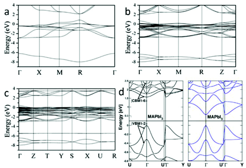 | ||
| Fig. 3 Electronic band structures of (a) cubic, (b) tetragonal, and (c) orthorhombic phases of MAPbI3 along the high-symmetry lines in the first Brillouin zone (reproduced with permission21). (d) Comparison of electronic band structures of MAPbI3 without (left) and with (right) the spin–orbit coupling interaction (reproduced with permission29). | ||
2.3 Unique charge separation and transport properties
Light-harvesting properties. A high optical absorption coefficient is undoubtedly crucial for a material’s PV application. A pure MAPbI3 layer possesses a linear absorption coefficient of 5.7 × 104 cm−1 at 600 nm wavelength of light,31 which is one order of magnitude higher than that of the N719 dye.27 The optical absorption coefficient of MAPbI3 is also higher than those of conventional inorganic PV materials such as GaAs, CdTe, and CIGS, evidenced by a calculation result (Fig. 4a).26 According to Wan-Jian Yin et al.'s work,26 the higher optical absorption coefficient of MAPbI3 originates from its direct band gap p–p transition feature. Because the CBM and VBM of MAPbI3 are mainly composed of Pb 6p orbitals and I 5p orbitals (which has been discussed above), the p–p transition is thus possible, which is generally much stronger than the p–s transition seen in CIGS, GaAs and so on. The p-orbital characterized CB minimum of MAPbI3 has a significantly higher density of states (DOS) than the s-orbital characterized CB minimums of GaAs, CdTe, CZTSe and CIGS (Fig. 4b). That leads to a remarkable difference in the joint density of states (JDOS) (Fig. 4c) which determines the optical absorption difference of these materials.26 A higher optical absorption directly leads to a higher efficiency of the solar cell with a comparatively thinner absorber layer (Fig. 4d), which will provide a shorter photogenerated carrier pathway and consequently leads to a lower recombination rate.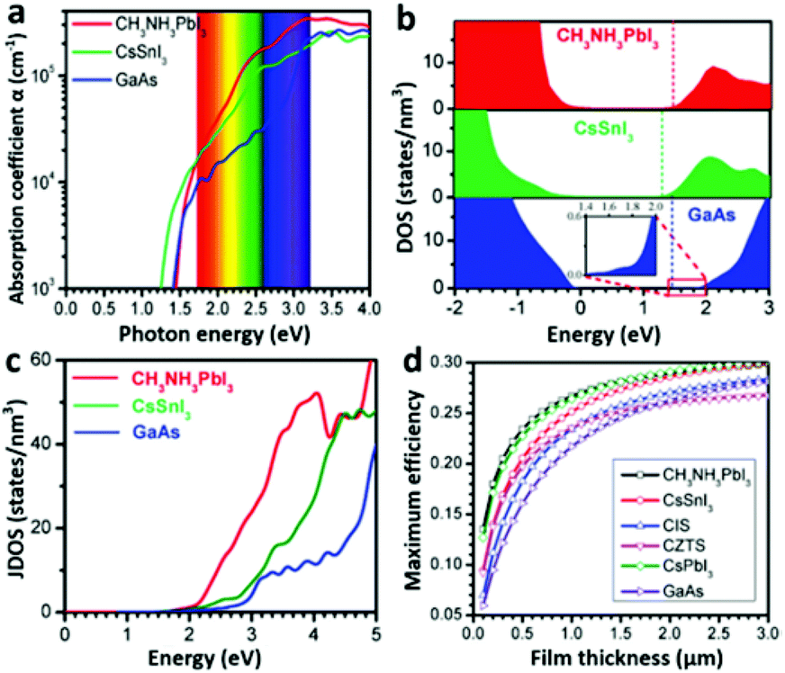 | ||
| Fig. 4 (a) The optical absorption, (b) DOS and (c) JDOS of MAPbI3, CsSnI3 and GaAs. (d) Calculated maximum efficiencies of MAPbI3, CIS, CZTS, and GaAs as a function of film thickness (adapted with permission26). | ||
Charge-transport properties. In addition to its excellent light harvesting properties, MAPbI3 is also characterized by efficient ambipolar electron and hole transport properties. Due to this, comparatively higher efficiencies are achieved even in PV devices without mesoporous n-type semiconductors32 or HTMs,33 which is impossible for the N719 dye based solar cell. The outstanding charge transport properties of perovskites can be clearly seen from their ultra-long balanced electron–hole diffusion length. Femtosecond transient optical spectroscopy has concretely evidenced that the electron–hole diffusion length of solution processed MAPbI3 is balanced to at least 100 nm, which is extremely long as to be comparable to the optical absorption length for λ ≤ 500 nm.31 For MAPbI3−xClx, the length even surpasses 1 μm.34 Long electron–hole diffusion lengths mean more electrons and holes can reach the perovskite cell electrodes and create an external electrical current. The ultra-long electron–hole diffusion lengths might be the main advantage of organic–inorganic halide perovskites. It is worth noting that photo-excitation of the perovskite leads to the generation of electron–hole pairs which exist as free carriers or excitons, and the thermal equilibrium of those species is eventually reached in the perovskite absorber. Presently, it is still unclear what charge carriers are dominantly attributed to the perovskite's exceptional properties of long diffusion lengths. However, the excitons in MAPbI3 belong to the Wannier–Mott type due to their large Bohr radii (22 Å). Their binding energy is calculated to be ∼50 meV according to the high frequency limit (ε∞ ≈ 6.5) at low temperature.35 At room temperature, the effective dielectric constant of MAPbI3 is notably increased because of the rotational motion of CH3NH3+ cations, which leads to a significantly enhanced screening effect of the Coulomb interaction between the electrons and holes. This screening effect further lowers the exciton binding energy to ca. 5 to 15 meV which is even smaller than kBT ∼ 26 meV (kB is the Boltzmann constant and T is the temperature) at room temperature. Thus the excitons are completely screened by the collective orientational motion of the organic cations, yielding almost free carriers at room temperature.36 This is totally different from the dyes usually used in DSSCs, which involve the formation of tightly bound excitons. Furthermore, excitons with such low binding energies in MAPbI3 are easy to be efficiently split at the interfaces in PV devices.
The electron–hole diffusion length of a material is directly determined by its mobility and lifetime of the charge carriers. On the one hand, the effective masses of photo-generated electrons and holes in MAPbI3 estimated by spin-polarized DFT calculations are m*e = 0.23m0 and m*h = 0.29m0, respectively.37 These values are comparable with those of silicon (m*e = 0.26m0, m*h = 0.29m0),26 and the hole effective mass is much smaller than those of CuInSe2 (m*h = 0.75m0)26 and CuInS2 (m*h = 1.3m0),38 and is comparable with those of Cu2ZnSnSe4 (m*h = 0.26m0),26 GaAs (m*h = 0.34m0)26 and CdTe (m*h = 0.28m0).26,39 The small hole effective mass of MAPbI3 can be deduced from its large dispersion of the VBM (Fig. 3), which is greatly enhanced by the antibonding coupling effect between the Pb lone-pair 6s2 orbitals and I 5p orbitals.26 The small effective masses of the photo-generated carriers lead to a high mobility (over 11 cm2 V−1 s−1).37 On the other hand, an extremely low charge carrier recombination rate of perovskites has been characterized by Snaith using transient THz spectroscopy, which reflects a long lifetime of their charge carriers.40 Furthermore, benign grain boundaries as evidenced by first-principle calculations, also account for their long charge carrier lifetimes. Calculation results show that all the defects that create deep levels have high formation energies, while defects with low formation energies all have transition energies less than 0.05 eV above (below) the VBM (CBM), forming shallow levels.41 In addition, grain boundaries (GBs) in the polycrystalline MAPbI3 layer do not generate any deep states in its band gap, resembling the above shallow effects.26
Though we have some distinct hints at their physical properties by calculations, why organic–inorganic halide perovskites have such long electron–hole diffusion lengths remains unclear. The unique structural properties of organic–inorganic halide perovskites might be the reason. The size of the organic cation is able to induce stress or confinement effects that can then determine the optoelectronic properties of the material itself. Though how these unique structural properties affect the charge separation and transport, and why these unique structural properties endow the materials with exceptional photoelectric properties remain open questions.
Huang et al. have proposed a simple model based on the crystal packing factor (PF) to evaluate the charge separation/transport abilities and photoelectric related properties of materials with similar compositions or structures.42–44 This simple model may shed some light on the reason for the exceptional photoelectric properties of the organic–inorganic halide perovskites. The concept came from Prof. John B. Goodenough's idea that lower elastic stiffness can promote distortion, which increases the internal field, and can be easily studied using the PF.45,46 A lower PF structure with lower elastic stiffness possesses a higher internal electric field, resulting in more efficient charge separation/transport and thus better photoelectric related properties.
In terms of carrier diffusion length, which is associated with the carrier lifetime and mobility, the PF model can provide good explanations for the better properties associated with a looser structure. An open structure (lower PF value) provides free space for atom vibrations, leading to a higher momentary polarizing field. The more polarizable structure results in a larger exciton Bohr radius, and hence a longer carrier lifetime. In addition, a lower PF structure is usually more deformable, which lowers the hopping barrier for polarons, thus increasing their mobility. The combination of increased carrier lifetime and mobility causes the higher charge separation/transport abilities. Some well-known photoelectric materials have very low PF values. Anatase TiO2 with excellent photocatalytic properties has a PF of 0.65;47–49 BiFeO3,50,51 Bi2FeCrO6 (whose PCE has reached 8.1% very recently)52 and KBiFe2O5![[thin space (1/6-em)]](https://www.rsc.org/images/entities/char_2009.gif) 53 with excellent ferroic photovoltaic properties have PFs of 0.66, 0.61 and 0.56, respectively. As for the organic–inorganic halide perovskites, we treat CH3NH3+ as one atomic ion for simplicity. The PFs of MAPbCl3, MAPbBr3, and MAPbI3 are deduced to be 0.58, 0.61 and 0.65 respectively, and these are extremely low as compared to the value of over 0.7 for most inorganic perovskites. If we consider the internal spatial openness of CH3NH3+, the PF should be even lower. The extreme structure-openness of organic–inorganic halide perovskites enables a large micro-deformation and/or spatial vibration in the local structure, which endows efficient electron–hole separation and charge transport, i.e., long charge carrier diffusion lengths.
53 with excellent ferroic photovoltaic properties have PFs of 0.66, 0.61 and 0.56, respectively. As for the organic–inorganic halide perovskites, we treat CH3NH3+ as one atomic ion for simplicity. The PFs of MAPbCl3, MAPbBr3, and MAPbI3 are deduced to be 0.58, 0.61 and 0.65 respectively, and these are extremely low as compared to the value of over 0.7 for most inorganic perovskites. If we consider the internal spatial openness of CH3NH3+, the PF should be even lower. The extreme structure-openness of organic–inorganic halide perovskites enables a large micro-deformation and/or spatial vibration in the local structure, which endows efficient electron–hole separation and charge transport, i.e., long charge carrier diffusion lengths.
Photo-ferroelectric properties. Additionally, carrier separation and transport in MAPbI3 based PV cells can be enhanced by a possible ferroelectric effect due to the electric dipole of the MA+ cation (i.e. [CH3]δ+–[NH3]δ−)54 and the distortion of the [PbI6]4− network. MA+ cations are non-uniformly located and rotate with high rates at room temperature.55 When an external electric field is applied, a transition from para- to ferroelectric molecular dipole order associated with the re-orientation of the [PbI6]4− network will occur in MAPbI3. Additionally, a novel photo-ferroelectric effect exists here.54 On the one hand, light excitation can facilitate the free rotation of MA+ cations by decreasing their binding energy to the [PbI6]4− cages;56 on the other hand, photoinduced carriers dramatically enhance the polarizability of the perovskite structure through intense electron–phonon coupling.57 Indeed, ferroelectric materials as a light absorbing layer have been employed in PV devices, in which the voltage output along the polarization direction can be significantly larger than the bandgap of the ferroelectric materials.58 The hysteresis of halide perovskites has been observed in resistivity measurements.59 The presence of ferroelectric domains in high-quality β-MAPbI3 thin films has been confirmed by piezoforce microscopy (PFM).60 Calculated results showed the presence of ferroelectric domains would result in internal junctions that may facilitate separation of photoexcited electron–hole pairs, and the reduction of recombination through segregation of charge carriers.55 Further experimental support is expected.
3 Progress in organometal halide perovskite based solar cells
So far plenty of research work has been reported with a focus on PSCs. Despite their diverse device architectures and constituent materials, PSCs are mainly composed of the following functional units: the transparent front electrode (usually FTO, ITO or AZO on glass or on a flexible polymer substrate), the perovskite light-absorber, two or one of the two auxiliary charge transfer units, i.e., the ETM (with or without mesoporous structure) and the HTM, and the counter electrode that has a proper work function >5.0 eV, including Au or Ag, Ni, as well as carbon materials.61–63 Next, we discuss in detail the perovskite-based PV device architectures, dynamic mechanisms, fabrication techniques and the materials of the perovskites, ETMs and HTMs. Finally, we end this section with some problems associated with measurement of the PSC performance.3.1 Progress in device architecture and landmark efficiencies
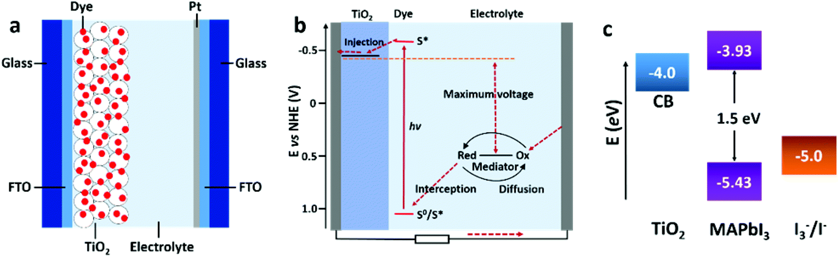 | ||
| Fig. 5 Schematic illustration of the general configuration (a) and working principle (b) of a DSSC (adapted with permission65). (c) The energy level diagram of TiO2, MAPbI3, and the redox couple of I3−/I− (adapted with permission4,27). | ||
Therefore, replacing the problematic liquid electrolytes with a solid-state HTM, i.e. fabricating all-solid solar cells, becomes an effective way to stabilize the perovskites and enhance the PV performance.
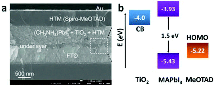 | ||
| Fig. 6 (a) Cross-sectional SEM image of the perovskite-based solid-state mesoscopic solar cell with spiro-MeOTAD as the HTM. (b) Energy level diagram of TiO2, MAPbI3, and spiro-MeOTAD (adapted with permission27). | ||
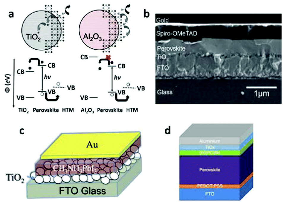 | ||
| Fig. 7 (a) Schematic illustration of the charge separation transport in a perovskite-sensitized TiO2 solar cell and a noninjecting Al2O3-based solar cell (reproduced with permission32). (b) Cross-sectional SEM image of a typical perovskite-based solid-state planar heterojunction solar cell (reproduced with permission68). Schematic illustration of a perovskite-based planar heterojunction PV device (c) without an HTM layer and (d) with an inverted structure (reproduced with permission72,77). | ||
This work revealed a surprising fact that perovskites do not form isolated quantum dots to serve as sensitizers, instead, they form a continuous film to effectively transport photo-generated carriers. The success of MSSC solar cells has driven explorations into planar thin film heterojunction PSCs, leaving out the preparation of the mesoporous n-type semiconductors.
An initial trial of planar thin film solar cells has been performed in Snaith's work,32 but with a relatively low efficiency of 1.8%. The difficulties in making planar cells may stem from the challenge of the deposition of a homogeneous pin-hole free perovskite layer with a high surface coverage, because the crystalline perovskite is likely to dewet or agglomerate upon annealing. With optimized film formation of the mixed halide MAPbI3−xClx, by controlling the atmosphere, annealing temperature, and film thickness, Snaith and co-workers68 obtained a high PCE of 11.4%, with an outstanding Jsc of 20.3 mA cm2 and Voc of 0.89 V. The typical configuration of a planar thin film cell is shown in Fig. 7b. The continuous perovskite film is in direct contact with the compact TiO2 layer and the HTM layer. Yang and co-workers69 reported a PCE of 12.1% with a low-temperature vapor-assisted solution process. Great success was achieved by Snaith's70 group with an ultrahigh PCE of 15.4%, Jsc of 21.5 mA cm2 and Voc of 1.07 V, utilizing a vapor-deposition process. This result strongly confirmed that perovskites can function in a simplified high efficiency device, without the need for any complex nanostructure. After that, the PCE of the perovskite planar heterojunction solar cell was improved to 15.7% by Kelly and his colleague,71 and was later boosted to 19.3% through contributions by Yang's group.5
After the excellent ambipolar transport properties of MAPbI3−xClx with electron–hole diffusion lengths exceeding 1 μm were experimentally confirmed,34 a hole conductor-free planar thin film cell became possible, in which efficient hole-transportation occurs simply through the perovskite layer. Indeed, using a simple heterojunction of MAPbI3/TiO2 (Fig. 7c), Etgar and his colleague72 achieved a PCE of 8%, with a high Jsc of 18.8 mA cm2, but relatively low Voc of 0.712 V. Very recently, the Grätzel group73 reported a printable hole conductor-free cell with a double layer of mesoporous TiO2 and ZrO2 as a scaffold infiltrated with perovskite. A special mixed-cation perovskite (5-AVA)x(MA)1−xPbI3 was utilized with a lower defect concentration and better pore filling as well as a more complete contact with the TiO2 scaffold. The cell achieved a PCE of 12.8% with a higher Voc of 0.858 V, and was stable for >1000 hours in ambient air under full sunlight.
PSCs could also be constructed with an inverted structure where the ETM is connected with the metal electrode and the HTM is deposited on the conductive glass, shown in Fig. 7d. A device with such structure commonly has an organic ETM (e.g. fullerene or its derivatives such as [6,6]-phenyl C61-butyric acid methyl ester (PCBM) or indene-C60 bisadduct (ICBA)) and an HTM made of poly (3,4-ethylenedioxythiophene) poly (styrenesulphonate) (PEDOT:PSS). A high efficiency of 12% was achieved with a device structure ITO/PEDOT:PSS/PolyTPD/MAPbI3/PCBM/Au where a perovskite layer was sandwiched between two organic charge-transport layers. Well defined energy levels in each layer resulted in effective charge transfer and collection, yielding a high performance device.74 The PCE of a device with the same structure was improved to 14.1% after incorporation of a LiF interlayer.75 By using an organic charge transport layer, flexible devices could be fabricated and a relatively high PCE of 9.2% has been achieved.76
3.2 Progress in dynamics and mechanisms
Despite the rapid progress in performance of PSCs, our understanding of the dynamics and underlying mechanisms of such devices has not proceeded at the same pace. As described above, successes have been achieved with various configurations of PSCs, such as perovskites on mesoporous n-type semiconductors, perovskites on mesoporous insulators, and perovskite-based planar thin film solar cells. Open questions thus exist on a series of topics: (i) are there significant differences among the working principles of the various configuration devices? (ii) What are the factors that significantly affect the device performance? Focusing on these questions, many efforts are underway to analyze the two primary successive steps in the various PV devices, i.e. the accumulation of photogenerated charge and charge separation. Elucidating those mechanisms is of fundamental importance in understanding the working principle of each type of PV device, and for their further optimization.The planar configuration device is expected to work by the following principle: the photo-generated excitons and free carriers co-exist in the perovskite layer and effectively transport along this layer due to the ambipolar charge transport properties of the perovskite. Electrons and holes are separately collected by the ETM and HTM layers. Recently, the mechanism of planar configured PSCs has been directly probed by direct measurement of the electron beam-induced current (EBIC) profiles of the device.78 The EBIC profile is useful for pinpointing the location of a driving force for charge separation, which is especially suited for determining the working principle of a photovoltaic device. In this technique, multiple electron–hole pairs are generated by the high-energy electron beam (as high energy photons do in the case of so-called multiple exciton generation). The EBIC signal is a current derived from the charge separation if there is any possible driving force.
A typical line scan of the HTM/MAPbI3−xClx/compact TiO2 solar cell is shown in Fig. 8b. It features two distinct peaks near the interfaces of HTM/MAPbI3−xClx and MAPbI3−xClx/compact TiO2, indicating the existence of two distinct built-in fields which are respectively associated with hole-extraction and electron-extraction. The decrease in the EBIC signal in the middle of the perovskite film results from all possible recombination events during carrier diffusion across the perovskite film to their preferred contact. These results provide direct experimental evidence of the p–i–n mode of operation of a perovskite-based planar thin film solar cell. Furthermore, this p–i–n model is composed of two separate hetero-junctions with higher electron-extraction efficiencies than that of hole-extraction, as seen from the different intensities of the two EBIC signal peaks. In consideration of the energy levels of the relevant material bands, a schematic band diagram of the cell can be constructed as illustrated in Fig. 8c, which is distinct from the homogenous built-in electric field (‘a-Si:H’-like) (Fig. 8d). The separate hetero-junction configuration works to minimize the dark current and maximize the photocurrent, and by their mutual contribution lead to an increased Voc.
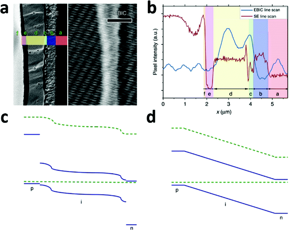 | ||
| Fig. 8 (a) Second electron (SE) image (left) and EBIC image (right) of the cross-section of the HTM/MAPbI3−xClx/compact TiO2 solar cell. Letters designate the different layers of the device: f, Au; e, HTM; d, MAPbI3−xClx; c, TiO2; b, FTO; a, glass. (b) SE and EBIC line scans at the indicated regions. A schematic diagram of the band energy in the (c) MAPbI3−xClx-based solar cell with a separated hetero-junction configuration and in the (d) ‘a-Si:H’-like solar cell with a homogeneous built-in electric field (adapted with permission78). | ||
EBIC signals with the same two-peak feature were observed in the cells employing insulated mesoporous oxide (cell configuration: HTM/MAPbI3−xClx on mesoporous Al2O3/compact TiO2), indicating that this kind of device also operates in p–i–n mode.78 However, in the absence of HTM, little field at the perovskite/Au junction was found and the active junction was located between the perovskite and the TiO2.78 That explains the comparatively lower Voc of the solar cell without HTM.
When tackling the working principle of PV devices with perovskites on mesoporous n-type semiconductors, e.g. TiO2, controversies are encountered: (i) whether this represents a sensitized or a heterojunction solar cell, i.e., whether electrons are injected from the perovskite into mesoporous TiO2, or just effectively transported through the perovskite itself; (ii) if the two pathways co-exist, which is more efficient and what is their ratio?
Moser, Grätzel and collaborators79 presented clear evidence of efficient electron injection from photoexcited MAPbI3 into TiO2, as well as evidence for efficient hole injection from photoexcited MAPbI3 into HTM. In this work, femtosecond pump-probe transient absorption experiments were carried out on MAPbI3 deposited on TiO2 and Al2O3 films, with and without HTM. The infrared probe allowed direct observation of the carrier's population decay within the perovskite itself, and the results are shown in Fig. 9a. The larger amplitude for the slower part of the decay observed for the perovskite on TiO2, compared to that of perovskite on Al2O3, indicated that some of the charges had already been separated through ultrafast electron injection into the TiO2 CB. Likewise, the hole injection process was evidenced by the fact that a larger amplitude was observed for the device with a HTM than the one without. Complementary evidence for electron injection from perovskite to TiO2 was obtained by time-resolved microwave photoconductance measurements.
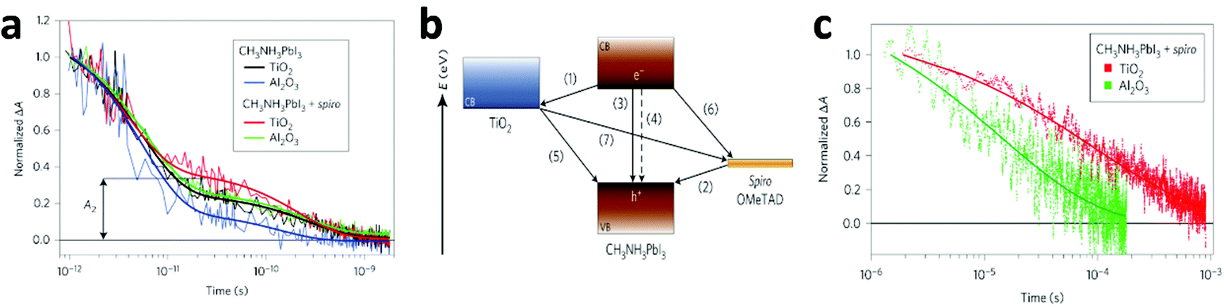 | ||
| Fig. 9 (a) Transient absorption signals of MAPbI3 in various systems measured at a probe wavelength of 1.4 μm following femtosecond laser pulsed excitation at 580 nm. Thick solid lines represent bi-exponential fits of experimental points starting at t = 1 ps. A2 represents the normalized absorbance change at 25 ps, used as a metric to compare the various samples. (b) Schematic illustration of the energy levels and charge transfer processes in the perovskite-sensitized solid-state solar cell. (c) Charge recombination dynamics obtained from nanosecond laser flash photolysis in the HTM-present devices MAPbI3/TiO2 (red) and MAPbI3/Al2O3 (green). The recombination is apparently slower when TiO2 is used than when Al2O3 is used. Thick lines represent a stretched exponential fit of the data (reproduced with permission79). | ||
In that work,79 the authors unravelled the mechanism of the charge transfer processes in this kind of solar cell, as illustrated as Fig. 9b. The desirable processes are (i) electron injection to TiO2 and (ii) hole injection to the HTM, which are the primary charge separation steps, followed by the transport of free electrons and holes respectively to their selective contacts. Undesirable processes include exciton annihilation in the perovskite itself – (iii) photoluminescence recombination and (iv) non-radiative recombination, and back charge transfer at three interfaces – (v) TiO2/perovskite, (vi) HTM/perovskite, and (vii) TiO2/perovskite at regions where the perovskite is absent. The kinetics of these processes are expected to determine the performance of the overall device. From the results of transient optical absorption spectroscopy in this work, the timescales of the above processes in the TiO2/perovskite/HTM configuration are estimated as follows: processes (i) and (ii) have comparable ultrafast femtosecond-to-picosecond timescales; nanosecond timescales were recorded for processes (iii) and (iv), but they were extensively suppressed due to the large amount of longer-lived charges caused by the efficient charge separation at the two interfaces; microsecond timescales for processes (v) to (vii). Therefore, the charge recombination processes ((iii) to (vii)) occur on a much slower timescale than the charge separation and extraction processes ((i) and (ii)), leading to the high performance of the PV device.
Grätzel and collaborators79 consider that the injection process is more efficient and preferable for higher device performance, thus charge recombination is shown to be significantly slower on TiO2 than on Al2O3 films (Fig. 9c), because electron injection is not thermodynamically feasible in Al2O3. However, a number of questions are yet to be answered. Snaith and co-workers32 showed an opposite result that charge collection in MAPbI3−xClx/Al2O3 devices is faster than in MAPbI3−xClx/TiO2, from transient photocurrent measurements. This indicates that the perovskite material itself is more efficient in transporting the negative charge than mesoporous TiO2. Recently, these controversies have been eased by the work of Cahen and co-workers.80 In this work, the EBIC measurements showed that holes are extracted significantly more efficiently than electrons in MAPbI3, while the diffusion lengths in MAPbI3−xClx are comparable for both charge types. That explains why MAPbI3-based cells require mesoporous electron conductors, while the MAPbI3−xClx-based ones do not. More interestingly, in MAPbI3−xClx-sensitized cells, the existence of two complementary paths for electron transport, involving either TiO2 or MAPbI3−xClx was also suggested.81 Zhu and co-workers82,83 showed almost overlapping curves for plots of the electron diffusion coefficient as a function of photoelectron density and recombination lifetime as a function of open-circuit voltage for mesostructured MAPbI3 and dye solar cells, indicating that the mechanistic factors governing the charge transport in MAPbI3/mesoporous-TiO2 based solar cells are similar to those in DSSCs. Therefore, transport in the perovskite cells is dominated by electron conduction within the TiO2 network rather than in the perovskite layer itself. The character of electron-injection from the perovskite to the ETM in PSCs was further confirmed by Snaith et al.84 and Grätzel et al.85 by means of impedance spectroscopy measurements. However, Bisquert et al.86 found that the photo-generated charges mainly accumulated in the MAPbI3 layer for the MAPbI3/mesoporous-TiO2 based PV device from impedance spectroscopy. This is essentially distinct from conventional DSSCs where instantaneous injection from the dye into the TiO2 occurs and no charge accumulation is observable in the light absorber. Additionally, their latter work87 demonstrated that the dominant carrier transport pathway is through the perovskite layer in the mesoscopically structured cell. Long carrier diffusion lengths (1 μm) were first measured by impedance spectra, and corresponded with the values for the perovskite layers obtained from time-resolved photoluminescence experiments.31
In summary, PSCs with planar configurations or with an insulated oxide scaffold work by a p–i–n model or a p–n model (devices without HTMs); the working principle for perovskite/mesoporous n-type semiconductor based solar cells is controversial, where the exact ratio of electrons injected into the mesoporous n-type semiconductor and those transported through the perovskite is unknown. Even so, the nanostructured scaffold at least has the following advantages: (i) it can provide a large area for the deposition of the perovskite light-absorber; (ii) it can prolong the light-absorption length; (iii) the perovskite film deposited on it is relatively thin, which can reduce the carrier transport length.
According to the working principles of the PSCs discussed above, the main factors that significantly affect the device's performance can be summarized as follows: the intrinsic material properties, such as the band gap, the energy levels of the CB and VB or HOMO and LUMO, and the charge transport properties; and the device parameters, such as the layer thickness, homogeneity, surface coverage degree, morphology, crystalline quality, contact quality of the different functional layers, density of defects, and so on. Therefore, the performance of the PV device can be optimized by tuning the composition of the materials and improving the fabrication techniques.
3.3 Progress in fabrication techniques
Generally, the fabrication of a complete PSC is based on a layer-by-layer process with the sequential deposition of the ETM on the front electrode substrate, followed by the deposition of the perovskite and HTM layers, and completed by the deposition of a noble metal counter electrode by a thermal evaporation method. Spin coating dominates the deposition process of the ETM and HTM, while hydrothermal in situ growth of TiO2 or ZnO is also feasible. However, the fabrication technique of the perovskite layer is versatile and has a crucial effect on the device performance.For the deposition of the perovskite layer, so far there have been four different methods: one-step solution deposition, two-step sequential solution deposition, the vapor-assisted solution process and dual-source vapor deposition. The first one is the simplest method which is most commonly used. The latter three methods possess particular merits in optimizing the perovskite film with respect to the crystallinity, morphology, and homogeneity. At the same time, solution-based methods to prepare perovskite nanoparticles88–90 have also been reported, which have potential application in the fabrication of PV devices.
:1) in aprotic polar solvents (γ-butyrolactone (GBL), dimethyl formamide (DMF), dimethyl sulfoxide (DMSO), N-2-methyl pyrrolidone (NMP), etc.) to get a clear solution. Secondly, the solution is spin-coated on the ready-prepared n-type contact layer. Finally, an annealing process at approximately 100 °C is needed to transform the precursor to crystalline perovskite. The deposition process must avoid moisture to prevent the decomposition of the perovskite. With this fabrication technique several parameters could be tuned to further optimize the device performance, such as the solvent and concentration of the precursor solution, thickness of the perovskite layer, and annealing temperature and time.
Snaith and co-workers68 have studied the effects of the annealing temperature and thickness on the morphology of the perovskite layer. Results show that as the annealing temperature increases, the number of pores in the final film decreases, while the surface coverage of the perovskite is also reduced due to the agglomeration process which results in perovskite islands. With increasing initial film thickness, the average pore size increases, while the surface coverage also increases. The optimized conditions are considered to be an annealing temperature of 90 °C and an initial perovskite film thickness of 450–550 nm. With these conditions, a uniform, fully-covered perovskite film without any pin holes can be fabricated. On the one hand, it enables the collection of a higher fraction of incident photons, which leads to a higher Jsc; on the other hand, the increased coverage removes a shunt path to avoid leakage currents, leading to a higher FF and Voc. In their later interesting work,91 leveraging the dewetting of perovskite films to form microstructured arrays of “islands”, they fabricated neutral colored semitransparent solar cells where the islands were thick enough to absorb all visible light, whereas the void space was visibly transparent. The preparation atmosphere, precursor solvent and the film annealing temperature were well controlled in their work. Grätzel's group92 also studied the annealing temperature effects on the perovskite film with a precursor solution of PbCl2 and MAI (1:3 molar ratio) in DMF. They found that complete conversion into the desired perovskite phase requires a temperature of at least 80 °C, and a sufficiently higher temperature is required for the crystallization of the perovskite material. However, too high an annealing temperature (above 140 °C) leads to the additional formation of PbI2, which will decrease the light absorption and hinder the injection of charges to and from TiO2, leading to poor Jsc, Voc and FF values. Conings and co-workers93 exploited DMSO as the solvent to prepare a perovskite precursor of high concentration up to 60 wt%. With this precursor, they yielded reasonably smooth perovskite films with up to >95% coverage and thicknesses exceeding 200 nm, thus enabling light absorption close to 100%, resulting in very reproducible and higher efficiency values (especially higher Jsc values) compared to the devices made from low-concentration precursors.
 | ||
| Fig. 10 Schematic diagram of a dual-source thermal evaporation method for depositing the perovskite absorbers (reproduced with permission70). | ||
3.4 Progress in perovskite, ETM and HTM materials
![[double bond, length as m-dash]](https://www.rsc.org/images/entities/char_e001.gif) CHNH3+ (FA+), CH3NH3+ (MA+) and Cs+, there is a symmetry lowering trend: FAPbI3 > MAPbI3 > CsPbI3. That is because the Pb–I–Pb bridging angles gradually deviate from the ideal linear conformation from FAPbI3 to CsPbI3, resulting in a reduction in orbital overlap of Pb–I. Thus a corresponding band gap widening trend is encountered: FAPbI3 < MAPbI3 < CsPbI3.59 By the design of a mixture of FA+ and MA+ in the A site, the optical-absorption onset of MAxFA1−xPbI3 will red shift compared to that of MAPbI3 (Fig. 11a), thus an enhanced solar-light harvesting property is expected. Furthermore, MAxFA1−xPbI3 exhibits a superior carrier-collection efficiency than the single-cation analogues, due to its longer exciton lifetime.95 Although FA+-based perovskites have narrower band gaps, they suffer from instability to a greater extent than MA+-based ones. Very recently, by rational incorporation of MAPbBr3 into FAPbI3, a stable and efficient mixed-perovskite light-harvesting layer was obtained, which improved the device PCE to 18%.98
CHNH3+ (FA+), CH3NH3+ (MA+) and Cs+, there is a symmetry lowering trend: FAPbI3 > MAPbI3 > CsPbI3. That is because the Pb–I–Pb bridging angles gradually deviate from the ideal linear conformation from FAPbI3 to CsPbI3, resulting in a reduction in orbital overlap of Pb–I. Thus a corresponding band gap widening trend is encountered: FAPbI3 < MAPbI3 < CsPbI3.59 By the design of a mixture of FA+ and MA+ in the A site, the optical-absorption onset of MAxFA1−xPbI3 will red shift compared to that of MAPbI3 (Fig. 11a), thus an enhanced solar-light harvesting property is expected. Furthermore, MAxFA1−xPbI3 exhibits a superior carrier-collection efficiency than the single-cation analogues, due to its longer exciton lifetime.95 Although FA+-based perovskites have narrower band gaps, they suffer from instability to a greater extent than MA+-based ones. Very recently, by rational incorporation of MAPbBr3 into FAPbI3, a stable and efficient mixed-perovskite light-harvesting layer was obtained, which improved the device PCE to 18%.98
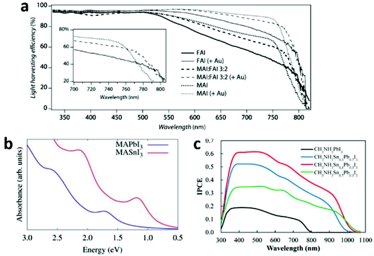 | ||
| Fig. 11 (a) Light-harvesting efficiency of MAxFA1−xPbI3 (reproduced with permission95). (b) Comparison between the relativistic GW calculated light absorption spectra of MASnI3 and MAPbI3 (reproduced with permission30). (c) IPCE curves for MASnxPb1−xI3 based solar cells (reproduced with permission99). | ||
Different M metal cations. The band gap of AMI3 differs distinctly with different M ions (e.g. Ge2+, Sn2+ and Pb2+), following the trend AGeI3 < ASnI3 < APbI3. This is consistent with the energy level trend Ge 4p < Sn 5p < Pb 6p. Apparently, Sn based halide perovskites are seemingly more suitable for PV application than Pb based ones, in light of their smaller band gaps and non-toxicity. Indeed, Sn based perovskites exhibit a larger extent absorption of visible light30 (Fig. 11b) and a large red-shift of the incident photon to current conversion efficiency (IPCE) curve edge99 (Fig. 11c). However, the efficiency was compromised by the poor Sn(II) stability.30,59 Relativistic GW calculations show that the different MASnI3 and MAPbI3 electronic properties are dominantly due to relativistic effects. These effects stabilize the MAPbI3 material towards oxidation, by inducing a deeper valence band edge and thus a wider band gap compared to MASnI3.30
Different X halide anions . Different halogens can significantly affect the band structure of MAPbX3 (e.g., the VBM sates, band gap). From Cl to Br to I, the band gap of MAPbX3 is gradually decreased, resulting in a gradual red shift of the optical-absorption edge, which is due to the fact that the VBM for MAPbX3 is mainly dominant by the X p orbital and minor hybridized states of lead with halide.21,25 Their VBM states gradually upshift from Cl to Br to I. Mixed multi-halide anions in the perovskites allow for the continuous tuning of the band gap and the optical absorption to cover almost the entire visible spectrum100–104 (Fig. 12). It is worth mentioning that the band gap of MAPbI3 will increase after being mixed with Br or Cl, resulting in a decreased absorption of visible light and a lower short-circuit current density (Jsc). However, a wider band gap can generate a higher open-circuit voltage (Voc). That is the reason why MAPbBr3−xClx based PV cells exhibit an ultrahigh Voc (1.5 V), in spite of a relatively low Jsc (4 mA cm−2).103 On the other hand, the incorporation of Cl into MAPb(I1−xClx)3 is limited to relatively low concentration levels (below 3–4%), owing to the large difference in the ionic radii of Cl− and I− and the low calculated formation energy.25,105 More interestingly, nearly no band gap alteration after Cl was mixed into MAPbI3 was evidenced both experimentally and calculatively.32,105 In addition, compared to the single halide ion perovskite, the mixed ones are more stable, as well as being able to facilitate the charge transport.32,100,105,106 The electron-hole diffusion length of the mixed halide (MAPbI3−xClx) is found to be greater than 1 μm, which is an order of magnitude greater than that of MAPbI3.34 That is because MAPbI3−xClx (τe = 273 ± 7 ns) has a much longer recombination lifetime than that of MAPbI3 (only τe = 9.6 ± 0.3 ns).34 The excellent diffusion length of MAPbI3−xClx makes the use of thicker absorber layers become possible in order to harvest more light, and the nano or meso structures are no longer necessary.
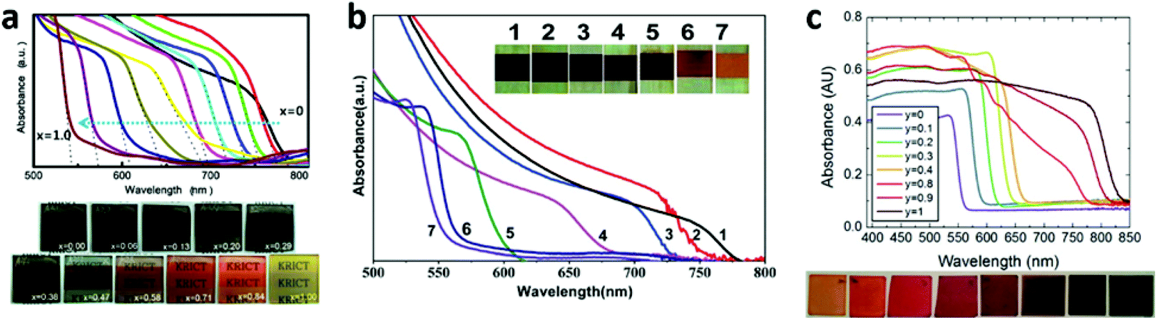 | ||
| Fig. 12 Photographs and UV-vis absorption spectra of MAPb(I1−xBrx)3 films made by (a) one-step solution deposition and (b) two-step sequential deposition. (c) Photographs and UV-vis absorption spectra of FAPbIyBr3−y films (reproduced with permission100–102). | ||
A mesoporous TiO2 scaffold deposited by a doctor blade method was initially introduced in the PSCs derived from the DSSCs. Good infiltration of the perovskite and the subsequent HTM into the pores of the mesoscopic scaffold is preferable for high performance devices. In the PV devices of Kim et al.27 increasing the TiO2 film thickness deteriorated the Voc and FF, which was attributed to an increase in dark current and electron transport resistance according to the impedance spectroscopic study. Meanwhile, the photocurrent density was not strongly influenced by a change in thickness of the TiO2 layer from 0.6–1.4 μm, maintaining a high level of 16–17 mA cm−2 due to the large optical absorption cross section. In the meantime, Etgar et al.107 fabricated mesoscopic MAPbI3/TiO2 heterojunction solar cells based on anatase TiO2 nanosheets exposing (001) facets with a side length of 30 nm and a thickness of 7 nm. The assembled simple MAPbI3/TiO2 cell showed a PCE of 5.5% under AM 1.5 solar light, which was relatively moderate due to the absence of a hole conductor material.
Afterwards, Kim et al.108 demonstrated the preparation of highly efficient PSC based on submicrometer (0.6 μm) rutile TiO2 nanorods. TiO2 nanorods were grown on the FTO-coated dense TiO2 layer substrates via a hydrothermal synthesis method, and their length was adjusted by setting different reaction times. Then the MAPbI3 and spiro-MeOTAD were subsequently spin-coated onto the TiO2 nanorod films. It was demonstrated that the well-ordered 1D structure of the shorter nanorod film was better for the infiltration of spiro-MeOTAD than the longer nanorod film with a disordered structure. Eventually, a PCE of 9.4% was achieved with an approximately 0.6 μm-thick rutile TiO2 nanorod film under one sun illumination, with a Jsc of 15.6 mA cm−2 and a Voc of 955 mV. Despite the significant reduction in surface area compared to the nanoparticle films, the resultant Jsc exceeded 15 mA cm−2 because of the high absorption coefficient of perovskite MAPbI3. Upon increasing the nanorod length, Jsc and Voc decreased to varying degrees. The decrease in Jsc upon increasing the nanorod length was likely to be related to either the amount of the adsorbed perovskite or the pore filling fraction, while the decrease in Voc was related to the different charge generation as explained by impedance spectroscopy. Xu et al.109 recently reported rutile nanowire-based PSCs with the highest efficiency of 11.7%. It was found that the best efficiency is achieved with 900 nm rutile single crystal nanowires, which provided a rapid electron transport pathway and subsequently led to the holes being the majority carrier in the perovskite phase. Jsc in this case was found to reach 22 mA cm−2. They also used photovoltage rising transient measurements to study the transport in the presence of recombination, which provided insights into the compromise between the conflicting demands of light harvesting and charge transport.
In 2014, freestanding TiO2 nanotube array films110 were first applied as electrodes in MAPbI3-based solar cells, which were prepared by a two-step anodization process and then detached from the substrate by in situ field-assisted chemical dissolution and transferred onto FTO that was covered by a TiO2 blocking layer. A sequential deposition approach was used to deposit the perovskite absorber into the nanotubes. MAPbI3 sensitized nanotube based electrodes had a significantly larger absorbance of visible light over the whole spectrum than nanoparticle based electrodes with the same thickness, ascribed to the enhanced light trapping ability of the nanotube arrays. Furthermore, charge recombination was effectively reduced in the nanotube based devices as indicated by photovoltage decay measurements. Therefore, the nanotube based cell yielded a higher PCE than the nanoparticle based one, with an equal Voc but a higher Jsc. The study of the dependence of photovoltaic performance on the nanotube film thickness showed that the photovoltaic performance increased with a decrease in the TiO2 nanotube film thickness, due to the different photoexcited charge extraction and collection efficiencies. A preliminary photovoltaic performance with a photocurrent density of 17.9 mA cm−2 and an efficiency of 6.52% was acquired from the cell with 2.3 μm TiO2 nanotubes.
Although TiO2 is commonly used as the electron transport layer and had appropriate energy levels for transferring electrons while blocking holes, its insufficient conductivity might lead to unnecessary ohmic losses or a nonideal space charge distribution within the cell. Photo-thermal deflection spectroscopy (PDS) measurements suggested that Al doping can reduce the number of sub-bandgap states of TiO2 and dramatically increase its electron conductivity.111 PSCs using compact TiO2 with an Al-doping level of 0.3 mol% delivered an enhanced Jsc value, leading to an improved PCE of 13.8%, compared with a PCE of 11.1% for the undoped compact layer. Y doping is another way to improve the conductivity of TiO2. Yang's group5 achieved a record PCE of 19.3% using Y-TiO2 as the ETM. A higher conductivity (2 × 10⁻⁵ S cm−1) for the Y-TiO2 film versus the undoped TiO2 film (6 × 10⁻⁶ S cm−1) was obtained due to the increased carrier concentration and the series resistance in the device was also reduced from 9.12 to 5.34 ohms. The improved conductivity of Y-TiO2 matched that of spiro-OMeTAD, 10-fold greater than that of pristine TiO2, which balanced the carrier transport to reduce nonideal space charge distribution. Previously, Qin et al.112 used mesoporous Y3+-substituted TiO2 (0.5% Y-TiO2) film to enhance the performance of PSCs. A PCE of 11.2% under simulated AM 1.5 full sun illumination was obtained, with a 15% improvement in Jsc compared with pure TiO2. Graphene insertion into the TiO2 layer is also an effective way to assist electron transport and improve the photovoltaic performance.31,113
ZnO is considered to be a viable alternative to TiO2 for PSCs due to its comparable energy levels as well as good electron transport properties. Kumar et al.114 reported a ZnO-based PSC, which is the foremost demonstration of PSCs employing the ZnO compact layer as a hole blocking layer and a mesoscopic scaffold layer as an electron transporter. The ZnO compact layer was formed by electrodeposition and ZnO nanorods were grown by chemical bath deposition, processed entirely at low temperature (<100 °C). The typical diameters of the ZnO nanorods grown on the ZnO film were in the range 100–150 nm and the lengths were between 400 and 500 nm. The blocking-ZnO/ZnO nanorod based PSC exhibited a remarkable PCE of 8.90% with a high Jsc of 16.98 mA cm−2, while the planar blocking-ZnO based cell without nanorods demonstrated a smaller PCE of 5.54% and Jsc of 11.27 mA cm−2. The increase in the Jsc value for the nanorod morphology could be attributed to better charge generation and collection efficiency due to increased light scattering and a larger heterojunction interface. Additionally, the mild conditions for the fabrication of the blocking-ZnO/ZnO nanorods allowed the processing of flexible PSCs. A PCE of 2.62% was achieved using blocking-ZnO/ZnO nanorod based cells on flexible PET/ITO substrates.
Similarly, in 2014, Son et al.115 reported an 11% efficient PSC based on ZnO nanorods. They prepared a ZnO seed layer by spin-coating and ZnO nanorods by a solution process. The diameter and length of the hexagonal ZnO nanorods were manipulated by controlling the concentration of the precursor solution and immersion time. After depositing the MAPbI3 absorber and spiro-MeOTAD HTM, the 82 nm wide and 1 μm long ZnO nanorod based PSC demonstrated a Jsc of 20.08 mA cm−2, Voc of 991 mV, FF of 0.56 and PCE of 11.13%, which is so far the highest efficiency for a ZnO nanorod based dye-sensitized PSC. It is noteworthy that the results were acquired in the absence of a compact TiO2 blocking layer, while the existing compact ZnO seed layer maybe serves as the substituted blocking layer. By contrast, a 1 μm long TiO2 nanorod film based cell was also prepared, resulting in values of Jsc = 20.92 mA cm−2, Voc = 869 mV, FF = 0.55 and PCE = 10.02%. The slightly higher PCE of the ZnO nanorod was due to the higher Voc associated with the higher conduction band position for ZnO than rutile TiO2 and the slower recombination characteristics, indicating that ZnO nanorods were an effective charge collection system in PSCs. Liu et al.71 reported a planar PSC using low temperature processed ZnO nanoparticles as the blocking layer. Impressive efficiencies of 15.7% on FTO and 10.2% on flexible ITO substrates were achieved. The high performance of these cells is considered to originate from the unconstrained MAPbI3 perovskite crystallite growth that occurs in the absence of a mesoporous scaffold.
Fullerene (C60) and its derivatives are another choice of ETM which have been widely used in organic or inorganic–organic hybrid solar cells. Chen et al.116 presented a hybrid organic solar cell (OSC) that used a planar heterojunction MAPbI3 perovskite/fullerene structure as the active layer, with a thin bathocuproine (BCP) film as a hole-blocking layer, achieving an optimized PCE of 3.0%. By applying PCBM or ICBA instead of C60, the PCEs can be optimized to 3.9% and 3.4%, respectively. These results verify the formation of a donor–acceptor interface at the MAPbI3/C60 heterojunction and the modulation of photovoltaic performance by acceptors of various LUMO levels. Snaith et al.84 used a self-assembled monolayer C60 functionalized mesoporous TiO2 as the “mesoporous electron acceptor” for an MAPbI3−xClx based solar cell, and a PCE of 6.7% was achieved. The C60 monolayer acts as an electron acceptor but inhibits further electron transfer into the TiO2 mesostructure, allowing a reduction of energy loss. This strategy opens an exciting and versatile route for hybrid PV devices. A perovskite/PCBM based flexible solar cell with a polymer substrate has been reported by Snaith's group,77 obtaining a PCE of 6%. Similarly configured devices have been fabricated by Bolink et al.,96 and the PCE was improved to 7%. These results demonstrate the versatility of the perovskite thin-film technology to the broad variety of possible device configurations.
Organic HTMs. Both small molecules and conducting polymers have been studied as novel substituent HTMs and a comparable photovoltaic performance with spiro-OMeTAD was achieved. Several functional polymers such as P3HT, PCDTBT and PTAA were introduced as electron blocking layers, among which PTAA performed best with a maximum PCE of 12.0%.67 Jeon et al.118 also used PTAA as the HTM layer and achieved a certified PCE of 16.2%. P3HT, a popular p-type conducting polymer usually used as an active layer in OPVs, attracted great attention as a candidate. Abrusci84 and Heo67 almost simultaneously reported P3HT as an HTM layer, and efficiencies of 3.8% and 6.7% could be achieved. The photovoltaic performance of a P3HT based solar cell could be further increased (from 9.2% to 12.4%)119 after doping P3HT with Li-TDSI and D-TBP. By sandwiching a hybrid perovskite film between selective contacts of TiO2 and P3HT layers, Conings93 and Giacomo120 also fabricated PSCs with efficiencies close to 10%. A comparative study of different HTMs, including spiro-OMeTAD, poly(3-hexylthiophene-2,5-diyl) (P3HT) and 4-(diethylamino)-benzaldehyde diphenylhydrazone (DEH), was conducted to investigate the various processes of charge transport and charge recombination.121 Hole transfer from perovskite to HTM under working conditions was demonstrated by photoinduced absorption spectroscopy. The difference in electron lifetime was revealed to explain the different device performance. The authors also suggested a design route to find new HTMs by controlling the perovskite–HTM interface together with matching energy levels.
Small molecules were also investigated as the HTM in PSCs. Spiro-OMeTAD doped with Li salts (LiTFSI) have already showed impressive performance as HTMs although long-term stability should be resolved.122 Modification of spiro-OMeTAD was realized by using spiro(TFSI)2 (a dicationic salt of spiro-OMeTAD) to increase the hole conductivity and operating stability.123 PSCs fabricated with spiro(TFSI)2 gave a PCE of 10% comparable to that of conventional spiro-OMeTAD.123 Considering the cost and stability issues associated with spiro-OMeTAD, the development of novel small molecule based HTMs is imperative. A pristine tetrathiafulvalene derivative (TTF-1) without p-type dopants has suitable HOMO and LUMO positions with respect to the energy levels of perovskite, as demonstrated by CV measurements.124 A PSC using TTF-1 as the HTM layer achieved a PCE of 11%, which was comparable to that of p-type doped spiro-OMeTAD (11.4%).125 An efficiency degradation comparison between TTF-1 and spiro-OMeTAD indicated that pristine TTF-1 performed better under ambient conditions with 40% humidity, and showed only a 20% efficiency decrease after a 500 h test. The enhanced durability was ascribed to avoidance of the use of sensitive additives and the hydrophobic effect of alkyl chains. In addition to TTF-1, PSCs fabricated with thiophene, quinolizino acridine and phenylamine derivatives as HTMs also exhibited impressive photovoltaic performance.126–128
Inorganic HTMs. To date, the organic HTMs used in PSCs have often suffered from high costs and low hole mobility. Exploring low cost and effective inorganic HTMs has attracted extensive attention. CuI was first demonstrated as an inorganic HTM in a PSC and a PCE of 6% was achieved.129 CuI, as the HTM layer, rendered the PV devices with a higher FF compared with those based on spiro-OMeTAD because of its higher electrical conductivity. The CuI based device also exhibited a better photocurrent stability than spiro-OMeTAD although the reason was unclear. However, the high charge recombination in the CuI layer limited the Voc. The solution to this problem could make CuI a competitive replacement for spiro-OMeTAD.129 Another copper based p-type semiconductor CuSCN can also be employed as the HTM layer because of its good transparency, high hole mobility and good chemical stability. PCEs of 3.8% and 6.4% were respectively obtained by Sarkar's group130 and Zaera's group131 using CuSCN as an HTM. After optimization of the perovskite layer morphology, a record PCE of 12.4% was achieved based on a CuSCN HTM.132 Another important p-type oxide, NiO, could also be used as a hole transport layer in PSCs, often with an inverted structure. With a thin NiO nanocrystalline film as the HTM layer, a PCE of 9.11% was achieved by Yang’ group.133 When mesoscopic NiO was used as a hole collecting electrode, a remarkable PCE of 9.51% was achieved.134 Electrodeposited NiO was also investigated as hole conductor in a planar inverted PSC and a maximum PCE of 7.3% was obtained.130 UV-treatment was able to deepen the work function of NiO, which led to a higher Voc of 1.05 V for the PSC.135 In addition, graphene oxide was also employed as a hole conductor in an inverted PSC and gave a PCE of over 12%.136
3.5 Problems associated with measurement of PSC performance
Hysteresis in the current–voltage (J–V) curves of PSCs is gaining scientific attention, owing to its blockage of the measurement of the steady-state power output, i.e. the real efficiency of the PSC. Hysteresis always manifests itself as a mismatch of the J–V curves scanned in the forward (from short-circuit to open-circuit) and reverse (from open-circuit to short-circuit) directions. It is also observed in other typical PV devices like DSSCs,137 CIGS, CdTe and amorphous silicon based solar cells,138,139 and its origin is considered to lie in the chemical capacitance which can be charged up under forward scan (FS) and discharged under reverse scan (RS), resulting in a reduced external FS-photocurrent and increased RS-photocurrent.140 In those typical PV devices, hysteresis can be effectively suppressed by lower the scan rate. However, hysteresis in the PSC is anomalous, in that it gets more extreme as the scan rate is reduced, and even exists at very slow scan rates (e.g. 0.011 V s−1).140 The steady state power output can be obtained only by a stepwise J–V measurement with a delay timescale of many seconds, shown in Fig. 13.141–143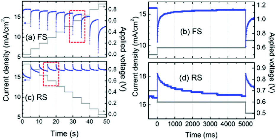 | ||
| Fig. 13 Photocurrent profile dependent on time during the (a) forward scan (FS) and (c) reverse scan (RS) at a stepwise voltage sweep between 0 and 0.9 V. Time-dependent current response at an applied voltage of 0.6 V (shown in dashed-red rectangles) during the (b) FS and (d) RS. Reproduced with permission.142 | ||
Snaith et al.140 initially suggested three possible origins for the hysteresis in the PSC: (1) defects in the perovskite or interface states which can act as traps for electrons and holes; (2) the ferroelectric properties of the perovskite; (3) the migration of excess ions. However, when considering the unusually long transient time in the stepwise J–V curves (Fig. 13), the possible origins of (1) and (3) seem to be unsatisfactory. Moreover, the possibility of the interfacial-trap origin is impossible for the fact that the planar thin film PSC exhibits a larger hysteresis than the mesoporous TiO2 based one whose interfacial traps are supposed to be more significant.141 So the most likely origin of the hysteresis associated with the transient effects is the ferroelectric properties of the perovskite itself. The underestimated efficiency derived from the FS-curve results from the excess polarization (with an opposite direction to the built-in electric field) and relatively small dielectric constant of the perovskite at the initial stage. The overestimated efficiency derived from the RS-curve results from the opposite effect.143
The ferroelectric polarization of the perovskite originates from the rotation of the MA+ and the distortions of the inorganic framework which are able to align themselves with the external electric field. The dielectric relaxation of such a structure is demonstrated to be an extremely slow process, especially for the realignment of the inorganic framework.56 That explains the long timescale of the transient effect (Fig. 13) which is consistent with the capacitance and the characteristic time obtained at low frequency in the impedance spectra (IS).57,144,145 The slow dielectric relaxation process can also explain the anomalous hysteresis that does not appear in the case of very fast scans, because the realignment of the perovskite cannot follow the higher scan velocity. Thus with a decrease of the scan velocity, the hysteresis becomes remarkable, unless a sufficiently slow scan (e.g. ≪0.01 V s−1) is employed to thoroughly eliminate the hysteresis.143 The ferroelectric properties of the perovskite could be significantly restrained by reduced crystal size because the small grain size could reduce the number of ferroelectric domain walls. That explains why mesoporous TiO2 based PSCs exhibits less pronounced hysteresis than planar thin film PSCs, owing to the small size confinement due to mesoporous TiO2.143,146 Moreover, the TiO2 layer is able to release the polarization effect in the perovskite through electron-injection, thus consequently reducing the hysteresis. The capacitance at low frequency in the IS decreases with increasing thickness of the TiO2 layer.142 The polarization properties of perovskite are also dependent on the growth conditions and the type of organic cations and halide ions.144
Additionally, light and voltage bias conditions prior to measurement can also have a significant impact upon the shape of the measured J–V curves and the apparent device efficiency. It has been demonstrated141,146 that pre-conditioning by light-soaking at forward bias is able to improve the FF and the photocurrent of the PSCs, leading to an apparently higher efficiency. It can also reduce the hysteretic effect in J–V curves. These effects can also be explained by the ferroelectric polarization of the perovskite, although some scientists have attributed these effects to ion migration.141 Illumination can dramatically increase the dielectric constant of the perovskite and decrease the energy barrier for the polarization alignment in the perovskite.56,57 Forward bias can generate an internal polarization field which points in the same direction as the photocurrent. Consequently, pre-conditioning by illumination and forward bias effectively facilitate charge separation and transport, leading to superior device performance. On the contrary, dark-soaking or reverse bias lead to opposite effects on the performance of PSCs.141,146
According to the analysis above, the measured J–V curves associated with the apparent efficiency of the PSC are greatly affected by various factors, such as the device structure, crystal size of the perovskite, selective contacts, measurement details, and pre-conditions. However, the real efficiency should only be obtained from the steady-state measurements regardless of any prior “history” of the device.140
4 Summary and outlook
Organic–inorganic hybrid PSCs are undergoing an evolutionary progress in the field of photovoltaics. The PCEs of this kind of solar cell have soared faster than any other competing solar technology in recent years147 (Fig. 14), as well as having the advantages of low cost and fabrication versatility. The powerful light-harvesting ability and excellent charge separation and transport capability of the perovskite could spark the design of next generation high performance PV devices. However, uncertainties still exist in the understanding of the working principles and the charge carrier dynamics of such devices, which may be the underlying breakthrough point for further improvements in their PV performance.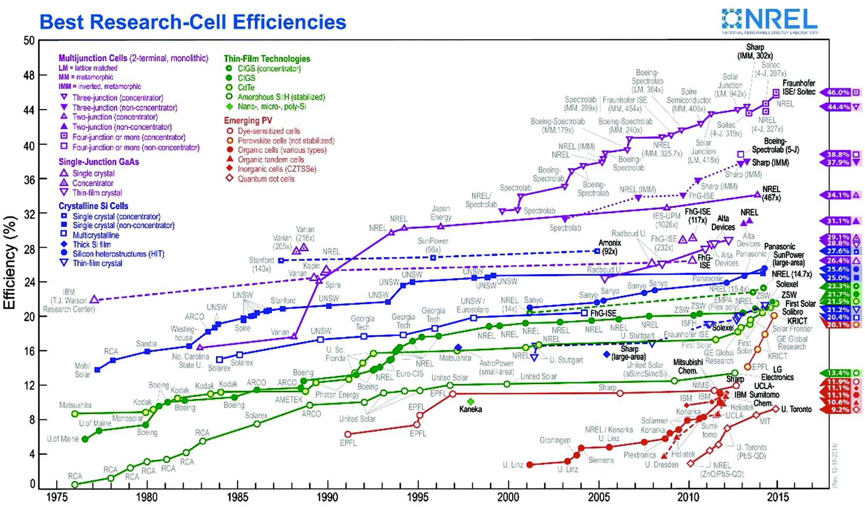 | ||
| Fig. 14 The rapid efficiency improvement of the PSCs compared to other PV technologies, data provided by the National Renewable Energy Laboratory (NREL) (reproduced with permission148). | ||
Hybrid tandem-junction solar cells are more attractive due to their better overall PCEs. Because of the success of PSCs with an inverted structure, tandem-junction type devices are now possible by matching the perovskite-based system with other thin-film technologies of silicon, CIS, CIGS, CZTSSe,149 as shown in Fig. 15.
 | ||
| Fig. 15 Schematic illustrations of conceptual hybrid tandem-junction PV devices (reproduced with permission149). | ||
The major impediment of the presently studied perovskites lie in their instability and the toxicity of Pb. The organic–inorganic hybrid halide perovskite is susceptible to moisture, the solution process, temperature and UV light radiation, which can greatly affect the composition and structure of the perovskite layer, and thus is detrimental to the charge separation and transport properties of the PV device.150 These factors have resulted in difficulties in the fabrication of the perovskite layer. Replacing Pb with Sn could be a possible way to eliminate the disadvantage of toxicity. Some remarkable progress has been seen in Sn based PSCs, although their performances are still lagging behind those of Pb-based ones, and the instability of Sn-based perovskites is a major challenge.99,151 Therefore, scalable technologies for industrial manufacture have to place emphasis on the stability and toxicity aspects. One more important question is whether these current perovskites are the best solar absorber materials and whether others will develop with much better performances than perovskite-type absorbers.
Overall, we believe it is promising to see the on-going efficiency improvements and the greater understanding of the material properties in the next few years, and the emergence of commercialized perovskite-based PV products might be on the horizon.
Acknowledgements
This work was financially supported by NSF of China (grant nos. 61376056, 51125006, 91122034, 61204072), and Science and Technology Commission of Shanghai (grant no. 13JC1405700, 14520722000).Notes and references
- B. O'Regan and M. Grfitzeli, Nature, 1991, 353, 737–740 CrossRef.
- A. Yella, H. W. Lee, H. N. Tsao, C. Yi, A. K. Chandiran, M. K. Nazeeruddin, E. W. Diau, C. Y. Yeh, S. M. Zakeeruddin and M. Gratzel, Science, 2011, 334, 629–634 CrossRef CAS PubMed.
- A. H. Ip, S. M. Thon, S. Hoogland, O. Voznyy, D. Zhitomirsky, R. Debnath, L. Levina, L. R. Rollny, G. H. Carey and A. Fischer, Nat. Nanotechnol., 2012, 7, 577–582 CrossRef CAS PubMed.
- A. Kojima, K. Teshima, Y. Shirai and T. Miyasaka, J. Am. Chem. Soc., 2009, 131, 6050–6051 CrossRef CAS PubMed.
- H. Zhou, Q. Chen, G. Li, S. Luo, T.-b. Song, H.-S. Duan, Z. Hong, J. You, Y. Liu and Y. Yang, Science, 2014, 345, 542–546 CrossRef CAS PubMed.
- P. Gao, M. Grätzel and M. K. Nazeeruddin, Energy Environ. Sci., 2014, 7, 2448 CAS.
- U. Schwarz, F. Wagner, K. Syassen and H. Hillebrecht, Phys. Rev. B: Condens. Matter, 1996, 53, 12545 CrossRef CAS.
- R. von Helmolt, J. Wecker, B. Holzapfel, L. Schultz and K. Samwer, Phys. Rev. Lett., 1993, 71, 2331 CrossRef CAS.
- J. Haeni, P. Irvin, W. Chang, R. Uecker, P. Reiche, Y. Li, S. Choudhury, W. Tian, M. Hawley and B. Craigo, Nature, 2004, 430, 758–761 CrossRef CAS PubMed.
- J. Suntivich, H. A. Gasteiger, N. Yabuuchi, H. Nakanishi, J. B. Goodenough and Y. Shao-Horn, Nat. Chem., 2011, 3, 546–550 CrossRef CAS PubMed.
- D. B. Mitzi, Prog. Inorg. Chem., 2007, 48, 1–121 CrossRef.
- D. B. Mitzi, C. Feild, W. Harrison and A. Guloy, Nature, 1994, 369, 467–469 CrossRef CAS.
- D. Mitzi, S. Wang, C. Feild, C. Chess and A. Guloy, Science, 1995, 267, 1473–1476 CrossRef CAS PubMed.
- C. Kagan, D. Mitzi and C. Dimitrakopoulos, Science, 1999, 286, 945–947 CrossRef CAS.
- X. Hong, T. Ishihara and A. Nurmikko, Solid State Commun., 1992, 84, 657–661 CrossRef CAS.
- J.-i. Fujisawa and T. Ishihara, Phys. Rev. B: Condens. Matter, 2004, 70, 113203 CrossRef.
- Z. Tang and A. M. Guloy, J. Am. Chem. Soc., 1999, 121, 452–453 CrossRef CAS.
- M. A. Green, K. Emery, Y. Hishikawa, W. Warta and E. D. Dunlop, Prog. Photovoltaics Res. Appl., 2012, 20, 12–20 CrossRef.
- C. Li, X. Lu, W. Ding, L. Feng, Y. Gao and Z. Guo, Acta Crystallogr., Sect. B: Struct. Sci., 2008, 64, 702–707 CrossRef CAS PubMed.
- A. Poglitsch and D. Weber, J. Chem. Phys., 1987, 87, 6373–6378 CrossRef CAS PubMed.
- T. Baikie, Y. Fang, J. M. Kadro, M. Schreyer, F. Wei, S. G. Mhaisalkar, M. Graetzel and T. J. White, J. Mater. Chem. A, 2013, 1, 5628–5641 CAS.
- J. J. Choi, X. Yang, Z. M. Norman, S. J. Billinge and J. S. Owen, Nano Lett., 2013, 14, 127–133 CrossRef PubMed.
- I. Koutselas, L. Ducasse and G. C. Papavassiliou, J. Phys.: Condens. Matter, 1996, 8, 1217 CrossRef CAS.
- T. Umebayashi, K. Asai, T. Kondo and A. Nakao, Phys. Rev. B: Condens. Matter, 2003, 67, 155405 CrossRef.
- E. Mosconi, A. Amat, M. K. Nazeeruddin, M. Grätzel and F. De Angelis, J. Phys. Chem. C, 2013, 117, 13902–13913 CAS.
- W. J. Yin, T. Shi and Y. Yan, Adv. Mater., 2014, 26, 4653–4658 CrossRef CAS PubMed.
- H.-S. Kim, C.-R. Lee, J.-H. Im, K.-B. Lee, T. Moehl, A. Marchioro, S.-J. Moon, R. Humphry-Baker, J.-H. Yum, J. E. Moser, M. Gratzel and N.-G. Park, Sci. Rep., 2012, 2, 591 Search PubMed.
- Y. Wang, T. Gould, J. F. Dobson, H. Zhang, H. Yang, X. Yao and H. Zhao, Phys. Chem. Chem. Phys., 2014, 16, 1424–1429 RSC.
- J. Even, L. Pedesseau, J.-M. Jancu and C. Katan, J. Phys. Chem. Lett., 2013, 4, 2999–3005 CrossRef CAS.
- P. Umari, E. Mosconi and F. De Angelis, Sci. Rep., 2014, 4, 4467 Search PubMed.
- G. Xing, N. Mathews, S. Sun, S. S. Lim, Y. M. Lam, M. Grätzel, S. Mhaisalkar and T. C. Sum, Science, 2013, 342, 344–347 CrossRef CAS PubMed.
- M. M. Lee, J. Teuscher, T. Miyasaka, T. N. Murakami and H. J. Snaith, Science, 2012, 338, 643–647 CrossRef CAS PubMed.
- L. Etgar, P. Gao, Z. Xue, Q. Peng, A. K. Chandiran, B. Liu, M. K. Nazeeruddin and M. Grätzel, J. Am. Chem. Soc., 2012, 134, 17396–17399 CrossRef CAS PubMed.
- S. D. Stranks, G. E. Eperon, G. Grancini, C. Menelaou, M. J. Alcocer, T. Leijtens, L. M. Herz, A. Petrozza and H. J. Snaith, Science, 2013, 342, 341–344 CrossRef CAS PubMed.
- K. Tanaka, T. Takahashi, T. Ban, T. Kondo, K. Uchida and N. Miura, Solid State Commun., 2003, 127, 619–623 CrossRef CAS.
- J. Even, L. Pedesseau and C. Katan, J. Phys. Chem. C, 2014, 118, 11566–11572 CAS.
- G. Giorgi, J.-I. Fujisawa, H. Segawa and K. Yamashita, J. Phys. Chem. Lett., 2013, 4, 4213–4216 CrossRef CAS.
- C. Czekelius, M. Hilgendorff, L. Spanhel, I. Bedja, M. Lerch, G. Müller, U. Bloeck, D.-S. Su and M. Giersig, Adv. Mater., 1999, 11, 643–646 CrossRef CAS.
- D. E. Gray, American institute of physics handbook, McGraw-Hill, 1982 Search PubMed.
- C. Wehrenfennig, G. E. Eperon, M. B. Johnston, H. J. Snaith and L. M. Herz, Adv. Mater., 2014, 26, 1584–1589 CrossRef CAS.
- W.-J. Yin, T. Shi and Y. Yan, Appl. Phys. Lett., 2014, 104, 063903 CrossRef PubMed.
- X. Lin, J. Wu, X. Lü, Z. Shan, W. Wang and F. Huang, Phys. Chem. Chem. Phys., 2009, 11, 10047–10052 RSC.
- X. Lin, F. Huang, W. Wang, Y. Wang, Y. Xia and J. Shi, Appl. Catal., A, 2006, 313, 218–223 CrossRef CAS PubMed.
- X. Lü, W. Yang, Z. Quan, T. Lin, L. Bai, L. Wang, F. Huang and Y. Zhao, J. Am. Chem. Soc., 2013, 136, 419–426 CrossRef PubMed.
- J. Goodenough and J.-S. Zhou, Chem. Mater., 1998, 10, 2980–2993 CrossRef CAS.
- J. Goodenough, N. Menyuk, K. Dwight and J. Kafalas, J. Phys. Colloq., 1971, 32, C1-622–C621-624 CrossRef.
- A. Fujishima, Nature, 1972, 238, 37–38 CrossRef CAS.
- T. Lin, C. Yang, Z. Wang, H. Yin, X. Lü, F. Huang, J. Lin, X. Xie and M. Jiang, Energy Environ. Sci., 2014, 7, 967–972 CAS.
- Z. Wang, C. Yang, T. Lin, H. Yin, P. Chen, D. Wan, F. Xu, F. Huang, J. Lin and X. Xie, Energy Environ. Sci., 2013, 6, 3007–3014 CAS.
- S. Yang, J. Seidel, S. Byrnes, P. Shafer, C.-H. Yang, M. Rossell, P. Yu, Y.-H. Chu, J. Scott and J. Ager, Nat. Nanotechnol., 2010, 5, 143–147 CrossRef CAS PubMed.
- M. Alexe and D. Hesse, Nat. Commun., 2011, 2, 256 CrossRef.
- R. Nechache, C. Harnagea, S. Li, L. Cardenas, W. Huang, J. Chakrabartty and F. Rosei, Nat. Photonics, 2015, 9, 61–67 CrossRef CAS.
- G. Zhang, H. Wu, G. Li, Q. Huang, C. Yang, F. Huang, F. Liao and J. Lin, Sci. Rep., 2013, 3, 1265 Search PubMed.
- F. Brivio, A. B. Walker and A. Walsh, APL. Mater., 2013, 1, 042111 CrossRef PubMed.
- J. M. Frost, K. T. Butler, F. Brivio, C. H. Hendon, M. van Schilfgaarde and A. Walsh, Nano Lett., 2014, 14, 2584–2590 CrossRef CAS PubMed.
- R. Gottesman, E. Haltzi, L. Gouda, S. Tirosh, Y. Bouhadana, A. Zaban, E. Mosconi and F. De Angelis, J. Phys. Chem. Lett., 2014, 5, 2662–2669 CrossRef CAS.
- E. J. Juarez-Perez, R. S. Sanchez, L. Badia, G. Garcia-Belmonte, Y. S. Kang, I. Mora-Sero and J. Bisquert, J. Phys. Chem. Lett., 2014, 5, 2390–2394 CrossRef CAS.
- Y. Yuan, Z. Xiao, B. Yang and J. Huang, J. Mater. Chem. A, 2014, 2, 6027–6041 CAS.
- C. C. Stoumpos, C. D. Malliakas and M. G. Kanatzidis, Inorg. Chem., 2013, 52, 9019–9038 CrossRef CAS PubMed.
- Y. Kutes, L. Ye, Y. Zhou, S. Pang, B. D. Huey and N. P. Padture, J. Phys. Chem. Lett., 2014, 5, 3335–3339 CrossRef CAS.
- Z. Ku, Y. Rong, M. Xu, T. Liu and H. Han, Sci. Rep., 2013, 3, 3132 Search PubMed.
- Z. Li, S. A. Kulkarni, P. P. Boix, E. Shi, A. Cao, K. Fu, S. K. Batabyal, J. Zhang, Q. Xiong and L. H. Wong, ACS Nano, 2014, 8, 6797–6804 CrossRef CAS PubMed.
- Q. Jiang, X. Sheng, B. Shi, X. Feng and T. Xu, J. Phys. Chem. C, 2014, 118, 25878–25883 CAS.
- J.-H. Im, C.-R. Lee, J.-W. Lee, S.-W. Park and N.-G. Park, Nanoscale, 2011, 3, 4088–4093 RSC.
- G. M, Nature, 2001, 414, 338–344 CrossRef PubMed.
- U. Bach, D. Lupo, P. Comte, J. Moser, F. Weissörtel, J. Salbeck, H. Spreitzer and M. Grätzel, Nature, 1998, 395, 583–585 CrossRef CAS PubMed.
- J. H. Heo, S. H. Im, J. H. Noh, T. N. Mandal, C.-S. Lim, J. A. Chang, Y. H. Lee, H.-j. Kim, A. Sarkar, M. K. Nazeeruddin, M. Gratzel and S. II Seok, Nat. Photonics, 2013, 7, 486–491 CrossRef CAS.
- G. E. Eperon, V. M. Burlakov, P. Docampo, A. Goriely and H. J. Snaith, Adv. Funct. Mater., 2014, 24, 151–157 CrossRef CAS.
- Q. Chen, H. Zhou, Z. Hong, S. Luo, H.-S. Duan, H.-H. Wang, Y. Liu, G. Li and Y. Yang, J. Am. Chem. Soc., 2013, 136, 622–625 CrossRef PubMed.
- M. Liu, M. B. Johnston and H. J. Snaith, Nature, 2013, 501, 395–398 CrossRef CAS PubMed.
- D. Liu and T. L. Kelly, Nat. Photonics, 2013, 8, 133–138 CrossRef.
- W. A. Laban and L. Etgar, Energy Environ. Sci., 2013, 6, 3249–3253 CAS.
- A. Mei, X. Li, L. Liu, Z. Ku, T. Liu, Y. Rong, M. Xu, M. Hu, J. Chen and Y. Yang, Science, 2014, 345, 295–298 CrossRef CAS PubMed.
- O. Malinkiewicz, A. Yella, Y. H. Lee, G. M. Espallargas, M. Graetzel, M. K. Nazeeruddin and H. J. Bolink, Nat. Photonics, 2014, 8, 128–132 CrossRef CAS.
- J. Seo, S. Park, Y. C. Kim, N. J. Jeon, J. H. Noh, S. C. Yoon and S. I. Seok, Energy Environ. Sci., 2014, 7, 2642–2646 CAS.
- J. You, Z. Hong, Y. Yang, Q. Chen, M. Cai, T.-B. Song, C.-C. Chen, S. Lu, Y. Liu and H. Zhou, ACS NANO, 2014, 8, 1674–1680 Search PubMed.
- P. Docampo, J. M. Ball, M. Darwich, G. E. Eperon and H. J. Snaith, Nat. Commun., 2013, 4, 2761 Search PubMed.
- E. Edri, S. Kirmayer, S. Mukhopadhyay, K. Gartsman, G. Hodes and D. Cahen, Nat. Commun., 2014, 5, 3461 Search PubMed.
- A. Marchioro, J. Teuscher, D. Friedrich, M. Kunst, R. Van De Krol, T. Moehl, M. Grätzel and J.-E. Moser, Nat. Photonics, 2014, 8, 250–255 CrossRef CAS.
- E. Edri, S. Kirmayer, A. Henning, S. Mukhopadhyay, K. Gartsman, Y. Rosenwaks, G. Hodes and D. Cahen, Nano Lett., 2014, 14, 1000–1004 CrossRef CAS PubMed.
- V. Roiati, S. Colella, G. Lerario, L. De Marco, A. Rizzo, A. Listorti and G. Gigli, Energy Environ. Sci., 2014, 7, 1889–1894 CAS.
- Y. Zhao, A. M. Nardes and K. Zhu, J. Phys. Chem. Lett., 2014, 5, 490–494 CrossRef CAS.
- Y. Zhao and K. Zhu, J. Phys. Chem. Lett., 2013, 4, 2880–2884 CrossRef CAS.
- A. Abrusci, S. D. Stranks, P. Docampo, H.-L. Yip, A. K.-Y. Jen and H. J. Snaith, Nano Lett., 2013, 13, 3124–3128 CrossRef CAS PubMed.
- A. Dualeh, T. Moehl, N. Tétreault, J. Teuscher, P. Gao, M. K. Nazeeruddin and M. Grätzel, ACS Nano, 2013, 8, 362–373 CrossRef PubMed.
- H.-S. Kim, I. Mora-Sero, V. Gonzalez-Pedro, F. Fabregat-Santiago, E. J. Juarez-Perez, N.-G. Park and J. Bisquert, Nat. Commun., 2013, 4, 2242 Search PubMed.
- V. Gonzalez-Pedro, E. J. Juarez-Perez, W.-S. Arsyad, E. M. Barea, F. Fabregat-Santiago, I. Mora-Sero and J. Bisquert, Nano Lett., 2014, 14, 888–893 CrossRef CAS PubMed.
- A. Kojima, M. Ikegami, K. Teshima and T. Miyasaka, Chem. Lett., 2012, 41, 397–399 CrossRef CAS.
- P. Audebert, G. Clavier, V. Alain-Rizzo, E. Deleporte, S. Zhang, J.-S. Lauret, G. Lanty and C. Boissiere, Chem. Mater., 2009, 21, 210–214 CrossRef CAS.
- L. C. Schmidt, A. Pertegás, S. González-Carrero, O. Malinkiewicz, S. Agouram, G. Mínguez Espallargas, H. J. Bolink, R. E. Galian and J. Pérez-Prieto, J. Am. Chem. Soc., 2014, 136, 850–853 CrossRef CAS PubMed.
- G. E. Eperon, V. M. Burlakov, A. Goriely and H. J. Snaith, ACS Nano, 2013, 8, 591–598 CrossRef PubMed.
- A. Dualeh, N. Tétreault, T. Moehl, P. Gao, M. K. Nazeeruddin and M. Grätzel, Adv. Funct. Mater., 2014, 24, 3250–3258 CrossRef CAS.
- B. Conings, L. Baeten, C. De Dobbelaere, J. D'Haen, J. Manca and H. G. Boyen, Adv. Mater., 2014, 26, 2041–2046 CrossRef CAS PubMed.
- J. Burschka, N. Pellet, S.-J. Moon, R. Humphry-Baker, P. Gao, M. K. Nazeeruddin and M. Grätzel, Nature, 2013, 499, 316–319 CrossRef CAS PubMed.
- N. Pellet, P. Gao, G. Gregori, T. Y. Yang, M. K. Nazeeruddin, J. Maier and M. Grätzel, Angew. Chem., Int. Ed., 2014, 53, 3151–3157 CrossRef CAS PubMed.
- C. Roldán-Carmona, O. Malinkiewicz, A. Soriano, G. M. Espallargas, A. Garcia, P. Reinecke, T. Kroyer, M. I. Dar, M. K. Nazeeruddin and H. J. Bolink, Energy Environ. Sci., 2014, 7, 994–997 Search PubMed.
- Q. Chen, H. Zhou, T.-B. Song, S. Luo, Z. Hong, H.-S. Duan, L. Dou, Y. Liu and Y. Yang, Nano Lett., 2014, 14, 4158–4163 CrossRef CAS PubMed.
- N. J. Jeon, J. H. Noh, W. S. Yang, Y. C. Kim, S. Ryu, J. Seo and S. I. Seok, Nature, 2015, 517, 476–480 CrossRef CAS PubMed.
- Y. Ogomi, A. Morita, S. Tsukamoto, T. Saitho, N. Fujikawa, Q. Shen, T. Toyoda, K. Yoshino, S. S. Pandey and T. Ma, J. Phys. Chem. Lett., 2014, 5, 1004–1011 CrossRef CAS.
- J. H. Noh, S. H. Im, J. H. Heo, T. N. Mandal and S. I. Seok, Nano Lett., 2013, 13, 1764–1769 CAS.
- S. A. Kulkarni, T. Baikie, P. P. Boix, N. Yantara, N. Mathews and S. Mhaisalkar, J. Mater. Chem. A, 2014, 2, 9221–9225 CAS.
- G. E. Eperon, S. D. Stranks, C. Menelaou, M. B. Johnston, L. M. Herz and H. J. Snaith, Energy Environ. Sci., 2014, 7, 982–988 CAS.
- E. Edri, S. Kirmayer, M. Kulbak, G. Hodes and D. Cahen, J. Phys. Chem. Lett., 2014, 5, 429–433 CrossRef CAS.
- N. Kitazawa, Y. Watanabe and Y. Nakamura, J. Mater. Sci., 2002, 37, 3585–3587 CrossRef CAS.
- S. Colella, E. Mosconi, P. Fedeli, A. Listorti, F. Gazza, F. Orlandi, P. Ferro, T. Besagni, A. Rizzo and G. Calestani, Chem. Mater., 2013, 25, 4613–4618 CrossRef CAS.
- J. M. Ball, M. M. Lee, A. Hey and H. J. Snaith, Energy Environ. Sci., 2013, 6, 1739–1743 CAS.
- L. Etgar, P. Gao, Z. Xue, Q. Peng, A. K. Chandiran, B. Liu, M. K. Nazeeruddin and M. Gratzel, J. Am. Chem. Soc., 2012, 134, 17396–17399 CrossRef CAS PubMed.
- H.-S. Kim, J.-W. Lee, N. Yantara, P. P. Boix, S. A. Kulkarni, S. Mhaisalkar, M. Grätzel and N.-G. Park, Nano Lett., 2013, 13, 2412–2417 CrossRef CAS PubMed.
- X. S. Qinglong Jiang, Y. Li, X. Feng and T. Xu, Chem. Commun., 2014, 50, 14720–14723 RSC.
- X. Gao, J. Li, J. Baker, Y. Hou, D. Guan, J. Chen and C. Yuan, Chem. Commun., 2014, 50, 6368–6371 RSC.
- S. K. Pathak, A. Abate, P. Ruckdeschel, B. Roose, K. C. Gödel, Y. Vaynzof, A. Santhala, S. I. Watanabe, D. J. Hollman and N. Noel, Adv. Funct. Mater., 2014, 24, 6046–6055 CrossRef CAS.
- P. Qin, A. L. Domanski, A. K. Chandiran, R. Berger, H.-J. Butt, M. I. Dar, T. Moehl, N. Tetreault, P. Gao and S. Ahmad, Nanoscale, 2014, 6, 1508–1514 RSC.
- Z. Zhu, J. Ma, Z. Wang, C. Mu, Z. Fan, L. Du, Y. Bai, L. Fan, H. Yan and D. L. Phillips, J. Am. Chem. Soc., 2014, 136, 3760–3763 CrossRef CAS PubMed.
- M. H. Kumar, N. Yantara, S. Dharani, M. Graetzel, S. Mhaisalkar, P. P. Boix and N. Mathews, Chem. Commun., 2013, 49, 11089–11091 RSC.
- D.-Y. Son, J.-H. Im, H.-S. Kim and N.-G. Park, J. Phys. Chem. C, 2014, 118, 16567–16573 CAS.
- J. Y. Jeng, Y. F. Chiang, M. H. Lee, S. R. Peng, T. F. Guo, P. Chen and T. C. Wen, Adv. Mater., 2013, 25, 3727–3732 CrossRef CAS PubMed.
- E. J. Juarez-Perez, M. Wuβler, F. Fabregat-Santiago, K. Lakus-Wollny, E. Mankel, T. Mayer, W. Jaegermann and I. Mora-Sero, J. Phys. Chem. Lett., 2014, 5, 680–685 CrossRef CAS.
- N. J. Jeon, H. G. Lee, Y. C. Kim, J. Seo, J. H. Noh, J. Lee and S. I. Seok, J. Am. Chem. Soc., 2014, 136, 7837–7840 CrossRef CAS PubMed.
- Y. Guo, C. Liu, K. Inoue, K. Harano, H. Tanaka and E. Nakamura, J. Mater. Chem. A, 2014, 2, 13827–13830 CAS.
- F. Di Giacomo, S. Razza, F. Matteocci, A. D'Epifanio, S. Licoccia, T. M. Brown and A. Di Carlo, J. Power Sources, 2014, 251, 152–156 CrossRef CAS PubMed.
- D. Bi, L. Yang, G. Boschloo, A. Hagfeldt and E. M. Johansson, J. Phys. Chem. Lett., 2013, 4, 1532–1536 CrossRef CAS.
- R. Schölin, M. H. Karlsson, S. K. Eriksson, H. Siegbahn, E. M. Johansson and H. Rensmo, J. Phys. Chem. C, 2012, 116, 26300–26305 Search PubMed.
- W. H. Nguyen, C. D. Bailie, E. L. Unger and M. D. McGehee, J. Am. Chem. Soc., 2014, 136, 10996–11001 CrossRef CAS PubMed.
- G. V. Tormos, M. G. Bakker, P. Wang, M. Lakshmikantham, M. P. Cava and R. M. Metzger, J. Am. Chem. Soc., 1995, 117, 8528–8535 CrossRef CAS.
- J. Liu, Y. Wu, C. Qin, X. Yang, T. Yasuda, A. Islam, K. Zhang, W. Peng, W. Chen and L. Han, Energy Environ. Sci., 2014, 7, 2963–2967 CAS.
- H. Li, K. Fu, A. Hagfeldt, M. Grätzel, S. G. Mhaisalkar and A. C. Grimsdale, Angew. Chem., Int. Ed., 2014, 53, 4085–4088 CrossRef CAS PubMed.
- P. Qin, H. Kast, M. K. Nazeeruddin, S. M. Zakeeruddin, A. Mishra, P. Bäuerle and M. Grätzel, Energy Environ. Sci., 2014, 7, 2981–2985 CAS.
- P. Qin, S. Paek, M. I. Dar, N. Pellet, J. Ko, M. Grätzel and M. K. Nazeeruddin, J. Am. Chem. Soc., 2014, 136, 8516–8519 CrossRef CAS PubMed.
- J. A. Christians, R. C. Fung and P. V. Kamat, J. Am. Chem. Soc., 2013, 136, 758–764 CrossRef PubMed.
- A. S. Subbiah, A. Halder, S. Ghosh, N. Mahuli, G. Hodes and S. K. Sarkar, J. Phys. Chem. Lett., 2014, 5, 1748–1753 CrossRef CAS.
- S. D. Chavhan, O. Miguel, H. J. Grande, V. Gonzalez-Pedro, R. S. Sánchez, E. M. Barea, I. Mora-Seró and R. T. Zaera, J. Mater. Chem. A, 2014, 2, 12754–12760 CAS.
- P. Qin, S. Tanaka, S. Ito, N. Tetreault, K. Manabe, H. Nishino, M. K. Nazeeruddin and M. Grätzel, Nat. Commun., 2014, 5, 3834 CAS.
- Z. Zhu, Y. Bai, T. Zhang, Z. Liu, X. Long, Z. Wei, Z. Wang, L. Zhang, J. Wang and F. Yan, Angew. Chem., Int. Ed., 2014, 126, 1–6 CrossRef.
- K.-C. Wang, J.-Y. Jeng, P.-S. Shen, Y.-C. Chang, E. W.-G. Diau, C.-H. Tsai, T.-Y. Chao, H.-C. Hsu, P.-Y. Lin and P. Chen, Sci. Rep., 2014, 4, 4756 Search PubMed.
- L. Hu, J. Peng, W. Wang, Z. Xia, J. Yuan, J. Lu, X. Huang, W. Ma, H. Song and W. Chen, ACS Photonics, 2014, 1, 547–553 CrossRef CAS.
- Z. Wu, S. Bai, J. Xiang, Z. Yuan, Y. Yang, W. Cui, X. Gao, Z. Liu, Y. Jin and B. Sun, Nanoscale, 2014, 6, 10505–10510 RSC.
- J. Bisquert, Phys. Chem. Chem. Phys., 2003, 5, 5360–5364 RSC.
- J. A. del Cueto, C. Deline, D. Albin, S. Rummel and A. Anderberg, A conference for new solar-based technologies. SPIE Solar Energy+ Technology, 2009 Search PubMed.
- M. Herman, M. Jankovec and M. Topič, Int. J. Photoenergy, 2012, 151452 Search PubMed.
- H. J. Snaith, A. Abate, J. M. Ball, G. E. Eperon, T. Leijtens, N. K. Noel, S. D. Stranks, J. T.-W. Wang, K. Wojciechowski and W. Zhang, J. Phys. Chem. Lett., 2014, 5, 1511–1515 CrossRef CAS.
- E. Unger, E. Hoke, C. Bailie, W. Nguyen, A. Bowring, T. Heumüller, M. Christoforo and M. McGehee, Energy Environ. Sci., 2014, 7, 3690–3698 CAS.
- H.-S. Kim and N.-G. Park, J. Phys. Chem. Lett., 2014, 5, 2927–2934 CrossRef CAS.
- J. Wei, Y. Zhao, H. Li, G. Li, J. Pan, D. Xu, Q. Zhao and D. Yu, J. Phys. Chem. Lett., 2014, 5, 3937–3945 CrossRef CAS.
- R. S. Sanchez, V. Gonzalez-Pedro, J.-W. Lee, N.-G. Park, Y. S. Kang, I. Mora-Sero and J. Bisquert, J. Phys. Chem. Lett., 2014, 5, 2357–2363 CrossRef CAS.
- J. Bisquert, L. Bertoluzzi, I. Mora-Sero and G. Garcia-Belmonte, J. Phys. Chem. C, 2014, 118, 18983–18991 CAS.
- H.-W. Chen, N. Sakai, M. Ikegami and T. Miyasaka, J. Phys. Chem. Lett., 2015, 6, 164–169 CrossRef CAS.
- R. F. Service, Science, 2013, 342, 794–797 CrossRef CAS PubMed.
- http://www.nrel.gov/ncpv/images/efficiency_chart.jpg .
- H. J. Snaith, J. Phys. Chem. Lett., 2013, 4, 3623–3630 CrossRef CAS.
- G. Niu, X. Guo and L. Wang, J. Mater. Chem. A, 2015 10.1039/c4ta04994b.
- F. Hao, C. C. Stoumpos, D. H. Cao, R. P. Chang and M. G. Kanatzidis, Nat. Photonics, 2014, 8, 489–494 CrossRef CAS.
| This journal is © the Partner Organisations 2015 |