 Open Access Article
Dewetting dynamics of a gold film on graphene: implications for nanoparticle formation
Sadanandam
Namsani
and
Jayant K.
Singh
*
Department of Chemical Engineering, Indian Institute of Technology Kanpur, Kanpur-2018016, India. E-mail: jayantks@iitk.ac.in
First published on 7th September 2015
Abstract
The dynamics of dewetting of gold films on graphene surfaces is investigated using molecular dynamics simulation. The effect of temperature (973–1533 K), film diameter (30–40 nm) and film thickness (0.5–3 nm) on the dewetting mechanism, leading to the formation of nanoparticles, is reported. The dewetting behavior for films ≤5 Å is in contrast to the behavior seen for thicker films. The retraction velocity, in the order of ∼300 m s−1 for a 1 nm film, decreases with an increase in film thickness, whereas it increases with temperature. However at no point do nanoparticles detach from the surface within the temperature range considered in this work. We further investigated the self-assembly behavior of nanoparticles on graphene at different temperatures (673–1073 K). The process of self-assembly of gold nanoparticles is favorable at lower temperatures than at higher temperatures, based on the free-energy landscape analysis. Furthermore, the shape of an assembled structure is found to change from spherical to hexagonal, with a marked propensity towards an icosahedral structure based on the bond-orientational order parameters.
I. Introduction
The directed assembly of functional nanomaterials, using top-down and bottom-up techniques for controlling the patterns of the nanomaterials, is extremely useful in many micro and nanoscale electronic, optical and biological applications.1 The patterning of nanoparticles, apart from fabrication techniques, relies on the selected substrate and the interaction of nanoparticles with the substrate. One of the popular techniques to form metallic nanoparticles on substrates is via dewetting of metallic thin films, which has gained much attention due to their novel physical and chemical properties.2–4 Recent studies have used solid or liquid phase dewetting of the metal films for the directed self-assembly of metal nanoparticles to demonstrate novel functional properties, for example, plasmonics,5–7 optical,8 and magnetic9 properties. Rack et al.10 used pulse laser irradiation to study the dewetting and directed assembly process of nickel films in different initial shapes such as circles, triangles, and squares. The authors showed that the laser pulse induces instabilities in the edge of the nickel film, which can be modulated to direct assembly of the materials. Similarly, Wu et al.11 have shown the formation of ordered nanoparticle arrays due to pulse-laser-induced dewetting of Cu rings. The directed assembly of bimetallic nanoparticles such as Cu–Ni has also been demonstrated by dewetting induced through irradiation of laser pulses on nanoscale Cu–Ni metallic films.12In the last few years patterning of metal nanoparticles on graphene has gained increased attention due to their high-grade catalytic and electronic properties.13–16 The chemical inertness, high conductivity and large surface area of graphene make it a novel platform for composites.17 Decoration of the graphene surface with nanotubes,18,19 nanowires,20,21 and nanoparticles22,23 has shown to induce superior properties compared to individual components. Hence, the understanding of decorated particles on the graphene surface is of immense interest. For example, Hupalo et al.24 used experiments and density functional theory (DFT) to study graphene–Pb and graphene–Dy interactions in nanomaterials that have applications in gas sensors.
Recently, Fuentes-Cabrera et al.25 studied the dewetting behavior of Cu nanodisks and nanowires on graphite and graphene surfaces using molecular dynamics (MD) simulations. They showed that the nanodisks and wires dewet the surface and form nanodroplets, which in turn jump off the surface with a velocity of 140 m s−1. Moreover, the effect of surface roughness on the dewetting behavior of Cu nanodisks on a nanopillared graphene surface was studied using MD simulations by Li et al.26 These simulation studies showed that the carbon nanopillars on graphene promote the dewetting behavior of the Cu film compared to that of the bare graphene. The dewetting and detachment behavior of Pt nanofilms on the graphitic surface was also studied using MD.27 Dewetting of metal thin films leading to active metal nanoparticles on the graphene surface generated a new kind of SERS substrates known as graphene-mediated SERS (G-SERS),28 which has created enhanced interest in the study of graphene–metal nanohybrids. Recently, gold–graphene nanohybrids have also gained attention because of their potential in SERS,28 sensors29 and graphene-based plasmonic device applications. For example, Zhou et al.30,31 annealed a gold film in a furnace at different temperatures (973–1533 K) to generate gold nanoparticles on a graphene surface. The authors demonstrated that the resulting hybrid has superior SERS properties compared to graphene–gold film hybrids. Iyer et al.,32 on the other hand, annealed a gold film on graphene at different temperatures (373–673 K) to form plasmonic nanostructures, and reported an increased SERS enhancement with temperature. Habenicht et al.4 used a laser pulse technique to study the dewetting behavior of liquid triangle-shaped gold nanoparticles on graphene, where detachment of the gold particles was observed at 3129 K. The shape and size of the nanoparticles formed after annealing of the gold film on the graphene surface are shown to depend on temperature and film thickness. Zhou et al.31 showed that the hexagonal and triangular-shaped nanoparticles exhibit superior SERS properties compared to hexagonal-shaped nanoparticles alone on the graphene surface. This indicates that the control of the size and shape of nanoparticles is also important, as they affect the properties of the nanoparticle–graphene hybrid material. The interactions at the metal–graphene interface in the metal–graphene hybrid system play a major role in structure control and composite performance. As the properties of metal–graphene hybrids are highly sensitive to the type of metal contact with the graphene surface, it is essential to understand the growth of metal nanostructures on graphene surfaces. SERS properties are dependent on the changes in the substrate structure. However, the formation of gold nanoparticles on graphene is not well understood. Typically on graphene, as observed by Iyer et al.,32 heating of the gold film leads to the formation of nanoparticles, and graphene wraps around these nanoparticles to create wrinkles at the edges of the nanoparticles. Iyer et al.32 clearly pointed out that the localized structure of graphene around the nanoparticle has a direct effect on the SERS properties. In particular, gold nanoparticles within the wrapped wrinkled shape of the graphene are shown to exhibit enhanced SERS activity. Electron-beam-lithography-based deposition of a serial array of gold nanoparticles on graphene shows SERS enhancement in the resulting system.33 However, it was also observed that nanoparticles diffuse from their deposited location and subsequently agglomerate with neighboring nanoparticles, which is also not well understood.
As evident from the above, the formation of gold nanoparticles and their self-assembly on graphene are not well studied. Thus, we wish to evaluate gold nanostructures on graphene surfaces, and their agglomeration behavior during the annealing process. To this end, we present a detailed all-atom MD study at different temperatures to explain the nanoparticle formation and dewetting behavior of gold films of different thicknesses.
II. Model and methodology
All MD simulations in this work are performed using the LAMMPS package.34 Metal–graphene systems are non-trivial systems, which require a suitable force field for a realistic simulation. In order to capture the behavior of the metal, an accurate metal–graphene interaction is required. One approach is to use a modified Lennard-Jones potential model (or any suitable model) such that some macroscopic properties (such as contact angles) match with experimental values. While this is more popular for organic or aqueous systems on graphene, such an approach is difficult to implement due to non-availability of experimental data for metal–graphene systems. However, a simple mixing rule has been used for metal–graphene systems, as recently employed by Fuentes-Cabrera et al.25 for a Cu–graphene system. Another approach is deriving a force field using the data generated from an accurate DFT study. In this study, Au–Au and C–C interactions are modeled using the embedded-atom method (EAM)35 and optimized Tersoff36 potentials, respectively, which are well-tested models for the respective systems. The Au–C interactions are described using Buckingham potential based on our recent DFT work:37 | (1) |
In order to understand the effect of the size and thickness of the film on the dewetting behavior of gold on graphene, we have considered circular disks of gold films of different diameters (30 and 40 nm) and variable thickness (5–30 Å). The graphene sheet of size 45 × 45 nm is considered in this work. The number of atoms in the simulation systems of 30 and 40 nm-diameter films on the graphene surface are 164![[thin space (1/6-em)]](https://www.rsc.org/images/entities/char_2009.gif) 696 and 510
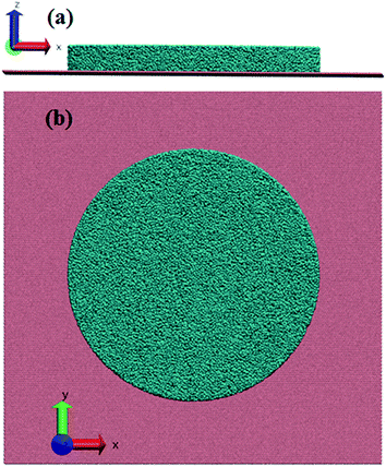
696 and 510![[thin space (1/6-em)]](https://www.rsc.org/images/entities/char_2009.gif) 925, respectively. Initially, bulk gold is simulated at different temperatures (973, 1073, 1400 and 1533 K) using an isobaric and isothermal (NPT) ensemble at 1 atm. Subsequently, gold nanodisks of desired diameter and thickness are generated from the final structure of bulk gold obtained from NPT simulations. All the generated nanodisks are placed on the surface of the graphene at a vertical distance of 0.3 nm and positioned in the middle of the graphene sheet. The top and side views of a typical initial structure used in simulations are shown in Fig. 1(a) and (b), respectively. To study the dewetting dynamics of the deposited gold film on graphene, NVT ensemble simulations are performed at 973, 1073, 1400 and 1533 K.
925, respectively. Initially, bulk gold is simulated at different temperatures (973, 1073, 1400 and 1533 K) using an isobaric and isothermal (NPT) ensemble at 1 atm. Subsequently, gold nanodisks of desired diameter and thickness are generated from the final structure of bulk gold obtained from NPT simulations. All the generated nanodisks are placed on the surface of the graphene at a vertical distance of 0.3 nm and positioned in the middle of the graphene sheet. The top and side views of a typical initial structure used in simulations are shown in Fig. 1(a) and (b), respectively. To study the dewetting dynamics of the deposited gold film on graphene, NVT ensemble simulations are performed at 973, 1073, 1400 and 1533 K.
The dewetting-induced density profile and retraction velocity of the gold film are calculated for gold nanodisks of different diameters and thicknesses at different temperatures. The retraction velocity of the film is defined as the dewetting-induced change in the film radius per unit time. We have also reported the velocity of the center of mass (CM) of the gold film in the z direction, perpendicular to the surface, which is defined as  where ZCM is the distance travelled by the CM of the gold film in the z direction. Inertia plays a dominant role in the dewetting process of liquid metals as they have low viscosity.2,4 The liquid retraction velocity at the boundary of the liquid thin film is described by Brochard-Wyart:45
| ν = (|S|ρ−1d−1)0.5, | (2) |
To understand the stability and self-assembly of gold nanoparticle structure formation on the graphene surface, we have calculated the free energy profiles for the gold-assembled structures. Upon heating the gold nanoparticle–graphene system at a particular temperature, the gold nanoparticles diffuse on the surface and form aggregates of different sizes. We use the population of definite cluster sizes of the assembled structures to calculate the free energy of the particular assembly. The free energy of the assembled structure of size k can be calculated using the following equation:46,47
 | (3) |
The bond orientation order parameter method is used identify the nanoparticle structure.51 For a considered bond r (a vector joining two neighboring atoms) the local bond order parameters are
| Qlm(r) ≡ Ylm(θ(r), ϕ(r)), | (4) |
 | (5) |
![[Q with combining macron]](https://www.rsc.org/images/entities/i_char_0051_0304.gif) lm is the average of Qlm(r) over all the bonds in the nanoparticle. The third order invariants are defined as
lm is the average of Qlm(r) over all the bonds in the nanoparticle. The third order invariants are defined as | (6) |
 | (7) |
We have used Q4, Q6, Ŵ4 and Ŵ6 values to identify the crystal structure of the nanoparticle formed upon annealing the gold film on the graphene surface. This analysis is useful in comparing the nanoparticle structures on the graphene surface with that of free nanoparticles.
III. Results and discussions
We start the discussion with the dewetting behavior of a 5 Å thick and 30 nm diameter gold film at 1073 K, which is shown in Fig. 2. It is well known that the dewetting begins at the edge of the film, where the surface tension is high.4,10 Upon heating the film breaks within 10 ps to form holes of different sizes in the middle of the film, leading to a cage-like structure. Subsequently, the growth of holes occurs, whereby the interior regions (holes) coalesce either with the interior gold patch or with the outside ring, leading to an increase in the thickness of the rim of the cage. The propagation and coalescence of holes are clearly seen during the period 20–30 ps; however, simultaneously the film also contracts toward its CM. With increase in time, the film further contracts on the surface (decay of holes), and the holes finally disappear at ∼40 ps. At ∼200 ps a stable spherical gold nanodrop forms on the graphene surface. During the contraction of the film, it is noted that the CM of the film moves perpendicularly away from the graphene surface (z direction) until 90 ps. Subsequently, the CM moves towards the surface. After 200 ps the gold nanodrop settles on the surface with no change in the CM. Similar behavior was also observed for a Cu film on a graphene surface25,26 and a Pt nanofilm on a graphitic surface.27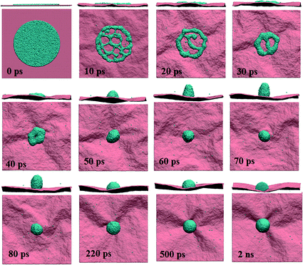 | ||
| Fig. 2 MD simulation snapshots of the 30 nm diameter gold film of thickness 5 Å on a graphene surface at 1073 K. | ||
The morphology and sequence of evolution depend on the nature of the surface, surface–film interactions and film thickness, which are well known for polymeric systems.52 To understand the effect of the thickness of the gold film on the dewetting process, we increase the film thickness from 5 to 10 Å. Fig. 3 shows the snapshots at different timesteps. It is apparent that the behavior is completely different from that seen for the 5 Å case. In contrast to the 5 Å film, upon heating at 1073 K the 10 Å film does not undergo rupture. Therefore, no holes are observed during the dewetting of the film as observed for the case of the 5 Å film. Instead, dewetting sets in through direct contraction of the film on the surface. Similar dewetting behavior, i.e., hole formation in the 5 Å film and direct contraction in films of thickness >5 Å, were also observed in the dewetting process of Cu on graphene25 and pillared graphene26 surfaces, and Pt on a graphitic surface.27 Despite different behavior for the 10 Å film, the film CM movement in the z direction is akin to that seen for the case of the 5 Å film. Interestingly, the CMs of both the films, 5 and 10 Å, move away from the surface up to 70 ps. Subsequently the film spreads, leading to a shift in the CM towards the surface. For both cases we observe a stable nanoparticle on the surface after 250 ps.
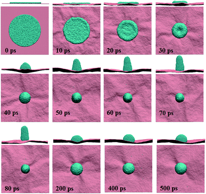 | ||
| Fig. 3 MD simulation snapshots of the 30 nm diameter gold film of thickness 10 Å on a graphene surface at 1073 K. | ||
In order to further compare the behavior of the gold film for two different thicknesses we analyze the variation in the atomic surface density along the x direction with simulation time at 1073 K, which is shown in Fig. 4(a) and (b), for 5 Å and 10 Å films, respectively. The decrease in the length of the film in the x direction shows the contraction of the film during the dewetting stage. The spread of the film on the surface decreases with time, and the density of the film rim increases due to retraction of the edge atoms towards the CM of the film during contraction. The fluctuations in Fig. 4(a) are indicative of the formation of holes, which diminishes by 40 ps due to decay of holes, as reflected in the two small peaks. Subsequently, the density increases due to film contraction up to ∼70 ps, as indicated by the single peak, signifying the formation of a nanodrop with a rod-like shape. After 70 ps the density of the film decreases with time; however, the base radius of the film on the surface increases, which indicates that the nanodrop spreads back on the surface. The spreading and rearrangement of the gold atoms continues until a stable nanoparticle forms at ∼250 ps.
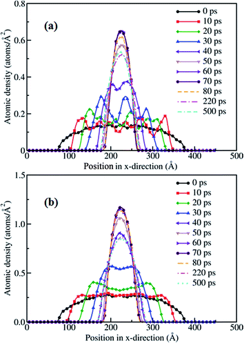 | ||
| Fig. 4 Surface atomic density profiles of the (a) 5 Å and (b) 10 Å gold films along the x direction at 1073 K. | ||
The dewetting behaviors of films at higher thicknesses, 15–30 Å, are akin to that seen for the 10 Å thick film, i.e., the nanodrop formation takes place due to the direct contraction of the film, and no hole formation is observed in all these cases. For all the thicknesses considered, 5, 10, 15, 20, 25 and 30 Å, the CM of the film moves away from the graphene surface up to ∼70 ps. Subsequently, the nanodrop returns to the surface and arranges itself to form a stable nanodrop at ∼250 ps. Based on the above discussion, it is evident that the sequence of evolution is dependent on the thickness, as hole formation ceases to exist for film thicknesses >5 Å. However, the formation of gold nanoparticles and their final structure on the graphene surface are independent of the film thickness. Similar behavior was also observed for the dewetting process of a mercury film on a glass slab.53
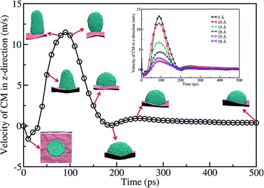
In the case of a Cu nanofilm on a graphene surface at 2200 K, which is significantly higher than its melting temperature 1358 K, the nanoparticles formed due to dewetting are shown to jump off the surface at a constant speed of 140 m s−1.25 However, the temperature considered in this work is close to the melting point of the gold. Fig. 5 presents a typical CM velocity profile of the gold film in the z direction at 1073 K, for the case of a 10 Å film. The CM velocity profile, along with the corresponding MD snapshots of the system, clearly shows that the velocity of the CM increases up to 90 ps and subsequently decreases. It is evident from the snapshots shown in Fig. 5 that the nanoparticle formed on the surface is in contact with the surface all the time during the dewetting process. The contraction of the gold film towards the CM of the film resulted in the formation of a rod-like shape at ∼70 ps, with an asphericity of ∼0.3 (lower than the perfect cylinder's value of 0.5). As the nanodrop moves towards the surface (from ∼70 ps to ∼250 ps) the shape gradually changes from a rod-like shape to a spherical crown-like shape. At ∼200 ps the nanodrop starts spreading on the surface. However, after 250 ps there is no change in the velocity, which shows a stable nanodrop formation on the surface, with an almost spherical shape (with an asphericity value of ∼0.026).
The dewetting behavior seen for 15, 20, 25, and 30 Å thick films at 1073 K is similar to that seen for the case of a 10 Å thick film. The film CM velocity profiles for 5, 10, 15, 20, 25, and 30 Å are shown as an inset in Fig. 5. The maximum velocity of the CM, for all the thicknesses, occurs within ∼80–90 ps. However, the magnitude of the velocity decreases with the increase in thickness. Moreover, for all the considered thicknesses of the film, a stable nanodrop forms at ∼250 ps. This shows that the timescale of nanoparticle formation is independent of the thickness of the film. However, the maximum CM velocity, where the spread of the nanodrop is at a minimum, decreases with the film thickness. Nevertheless, we do not observe any detachment of the gold nanoparticles at any instant from the graphene surface within the temperature range considered in this study.
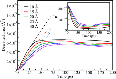
The dewetting-induced nanodrop formation involves three stages: contraction of the film, formation of a rod-like nanodrop and transformation of the rod-like nanodrop to a stable spherical nanodrop (see Fig. 5). To characterize the contraction of gold films on the surface we have calculated the dewetting area of the film. The dewetting area vs. time plot is shown in Fig. 6 for the case of a 15 nm diameter film on the graphene surface at 1073 K. The dewetted area (up to ∼40 ps), corresponding to the contraction stage of the process, is observed to vary with tα, where α is 0.87, 0.86, 0.96, 1.06 and 0.96 for 10, 15, 20, 25, 30 Å thickness films, respectively. This shows that the dewetted area of the film increases almost linearly with time during the contraction stage, and this is more prominent for thicker films. Similar linear variation of the dewetted area with time is also observed in the case of dewetting of thin polymer films.54 After ∼40 ps we do not observe a notable change in the dewetted area of the film. This indicates that during the process of rod-like shape formation and further transformation to spherical nanodrops the dewetted area does not change significantly. The inset of Fig. 6 shows a corresponding decreasing trend of the square radius of the film with time, as expected from the behavior of the dewetted area. Similar behavior for the dewetted area or radius of the film is also observed at other temperatures (973 K, 1400 K and 1533 K).
In order to investigate the retraction behavior for a gold film on a graphene surface, we calculate the retraction velocity (change in radius of the film per unit time),53 for all the thicknesses considered in this study. The retraction velocity profiles are similar in nature to those of the CM velocity. The variation of maximum retraction velocity with film thickness is shown in Fig. 7. The retraction velocity increases with increase in temperature. On the other hand, the maximum retraction velocity decreases with the increase in film thickness. Similar behavior of decreasing retraction velocity with film thickness is also observed in the case of the Cu nanofilm25 and the triangle shaped-gold film4 dewetting on a graphene surface. However, at a temperature of 1533 K the retraction velocity of the 30 nm gold film of thickness 10 Å is ∼320 m s−1, which is significantly more than the maximum retraction velocity of 233 m s−1![[thin space (1/6-em)]](https://www.rsc.org/images/entities/char_2009.gif) 25 for the corresponding size of Cu film on a graphene surface at 2200 K. The higher retraction velocity of the gold film even at lower temperature may be attributed to its lower viscosity. It should be noted that the detachment of a Cu drop on graphene is observed at a temperature ∼1.6 times its melting temperature. Although the Au–graphene binding energy is lower (−0.886 eV) than that of Cu–graphene (−0.909 eV), the temperature considered for gold in this work is around its melting temperature, as motivated by the experimental conditions.55 We believe higher temperature would detach the gold drop, as seen for other metal–graphene cases.
25 for the corresponding size of Cu film on a graphene surface at 2200 K. The higher retraction velocity of the gold film even at lower temperature may be attributed to its lower viscosity. It should be noted that the detachment of a Cu drop on graphene is observed at a temperature ∼1.6 times its melting temperature. Although the Au–graphene binding energy is lower (−0.886 eV) than that of Cu–graphene (−0.909 eV), the temperature considered for gold in this work is around its melting temperature, as motivated by the experimental conditions.55 We believe higher temperature would detach the gold drop, as seen for other metal–graphene cases.
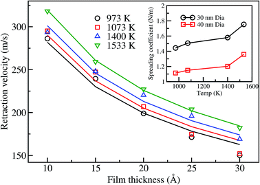 | ||
| Fig. 7 Variation of the retraction velocity with film thickness for a 30 nm film at different temperatures. Solid lines represent the theoretical velocity based on the fit of eqn (2) to the simulation data. The inset shows the spreading coefficient variation with temperature. | ||
Further, to study the system size effect on the dewetting behavior we have considered a gold disk of diameter 40 nm with different thicknesses (5, 10, 15, 20, 25, and 30 Å) on the graphene sheet. The dewetting behavior for the case of a 40 nm diameter film is more or less the same as that seen for the 30 nm diameter film. At a thickness of 5 Å, the 40 nm film dewets the surface forming nanoholes, which is not seen for thicker films, in line with the behavior seen for the 30 nm diameter films. However, its retraction behavior leading to nanoparticle formation is slightly different. The CM of the film moves in the z direction up to ∼160 ps in contrast to the 30 nm diameter film case. Moreover, the film forms a stable nanodrop on the surface at ∼450 ps. The time taken for the 40 nm film to form a stable nanodrop on the surface is more than the time taken for the case of the 30 nm gold film. This shows that the dewetting process is dependent on the diameter of the film. The retraction velocity profiles for the case of the 40 nm diameter films also follow a similar trend to that seen for the 30 nm film. This retraction velocity data also fits well with the theoretical velocity equation (2). Retraction velocity profiles for both the cases (30 and 40 nm diameter films) clearly show that the retraction velocity increases with increase in temperature.
Now, we turn our attention towards the spreading behavior of the nanodrop, which can be analyzed based on the variation of the spreading coefficient, |S|, with temperature. The spreading coefficient is the driving force for the dewetting process, and takes into account the capillary force contribution.53 In order to obtain the spreading coefficient, the theoretical velocity as shown in eqn (2) is fitted using the simulation data and is shown in the inset of Fig. 7. The absolute value of the spreading coefficient is found to increase with temperature, which is expected for the dewetting process. At low temperatures, |S| linearly increases with temperature until the melting temperature. Subsequently, the change in |S| is more drastic above the melting temperature, as seen for 1400 and 1533 K, indicating increased tendency for dewetting at higher temperature, which is also observed for the Cu-nanopillared surface system.56 The spreading values in this work are lower than that reported by Habenicht et al.,4 which is expected as the experiments performed by the authors were at a significantly higher temperature, 3129 K. It is also noted that an increase in the diameter of the film decreases the spreading coefficient, i.e., dewetting is slow for the 40 nm film compared to the smaller diameter film. This is primarily due to the increased radius of curvature for the 40 nm film edges, leading to the reduction in the surface tension forces. It is clear from the above that the increase in temperature and decrease in film diameter favor the dewetting of the film on the graphene surface. Similar behavior was also observed for other systems such as for a Cu-nanopillared surface26 and Pt–graphite,27 where increase in temperature also led to increase in the detachment velocity of the nanodrop.
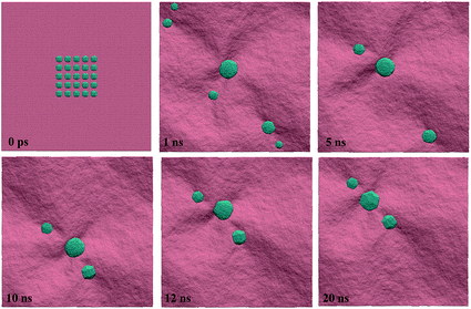
The dewetting of liquid metal leads to different shapes and sizes of nanoparticles on substrates, as observed by various researchers. For example, Zhou et al.31 observed different shapes and sizes of gold nanoparticles on graphene surfaces at different temperatures. Moreover, the substrate can promote or suppress diffusion of nanoparticles. For example, in the case of a silica substrate gold nanoparticles have much less diffusion compared to on a graphene substrate due to the weaker interactions in the gold–graphene system. Hence agglomeration behavior is promoted on graphene, as observed by Schedin et al.33 Such agglomeration behavior of nanoparticles can lead to extremely interesting structures, as seen in different systems.57,58 It is now well known that the shape and size of the gold nanoparticle greatly affects the SERS properties.31,32 Hence, to understand the aggregation behavior of gold nanoparticles on graphene, we consider 10 independent simulations, at different temperatures, with 25 nanoparticles of 2 nm diameter on a graphene surface. The nanoparticles diffuse and merge, leading to bigger agglomeration as the simulation runs. We track the agglomeration of nanoparticles using simple geometrical criteria, and using cluster size analysis we generate the free energy of the assembled structures as per eqn (3).
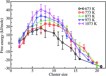
Fig. 8 shows the free energy profiles of different assembled structures calculated at 673, 773, 873, 973 and 1073 K. These profiles clearly show that there is a free energy barrier for the formation of an assembled structure of gold nanoparticles on a graphene surface, for all temperatures considered in this work. At 673 K the free energy barrier is about 15 kJ mol−1, and the critical cluster size is ∼k = 7. This indicates that ∼15 kJ mol−1 of energy is required to form an assembled structure of size 7. Once the critical cluster size is formed, subsequent growth is favorable to form a fully assembled structure. However, the largest cluster size obtained within 24 ns is 21, which is more stable than the single unassociated units by about 27 kJ mol−1. In contrast, at 773 K the free energy barrier is higher, ∼23 kJ mol−1, corresponding to a cluster size of 8. The final assembled structure of size 20, within 24 ns, is more stable than the single unassociated units by ∼23 kJ mol−1. Furthermore, the assembly of nanoparticles is unfavorable at 773 K by 8 kJ mol−1 when compared to the process at 673 K. The energy barrier for the formation of critical clusters is found to increase with increasing temperature. The corresponding energy barriers at 873, 973, and 1073 K are ∼26, ∼32, and ∼40 kJ mol−1, respectively. In other words, the self-assembly processes at 873, 973, and 1073 K are unfavorable by 11, 17 and 25 kJ mol−1, respectively, in comparison to the 673 K process. This analysis shows that the assembly of gold nanoparticles on the graphene surface is more favorable at low temperatures. The final assembled structures formed at 873, 973, and 1073 K, on the other hand, are more stable than the single unassociated nanoparticles by ∼23, 24 and 16 kJ mol−1, respectively.
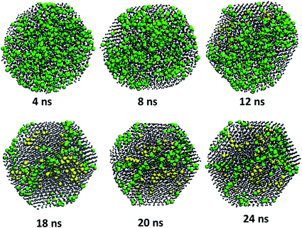
Fig. 9 displays the assembled structures formed on the graphene surface after annealing of one arrangement of nanoparticles on the graphene surface, at 1073 K. The final structure, however, does not change upon changing the initial structure (with the nearest neighbor nanoparticle–nanoparticle distance varying from 1 to 7 nm). Upon heating, the gold nanoparticles diffuse on the surface and form different sizes of aggregates on the surface. With time the size of the aggregates increases and the number density of clusters decreases. The aggregate structure however does not change beyond 5 ns, as apparent from Fig. 9. The nanoparticles formed at ∼5 ns on the graphene surface are spherical in shape. Between 5 and 12 ns we observe transformation of nanoparticles from spherical to hexagonal. Subsequently, the aggregates remain in the hexagonal shape, as seen in our simulations up to 24 ns. The behavior is similar in nature at different temperatures. The gold nanoparticles mainly in the hexagonal form were also observed in an experimental study by Zhou et al.31 However, the authors also reported the formation of triangular-shaped nanoparticles, which was seen to be temperature-dependent. In particular, at 873 and 973 K hexagonal particles were seen in the experiment, in line with our simulation work. At a higher temperature of 1073 K, a mixture of triangular and hexagonal-shaped nanoparticles was observed in the experiment, which is not seen in our simulations. We believe such structures may be metastable in nature, which we plan to investigate in our future work. In the experimental work of Zhou et al.,31 it was observed that the SERS enhancement was high at lower temperatures (873, 973 and 1073 K) compared to that seen at higher temperature (1100 K). This is due to well-faceted nanoparticle formation at lower temperatures. Although our study, based on classical MD simulations, does not provide direct reference to SERS data, we observe enhanced probability (lower energy barrier) of faceted nanoparticle formation with decreasing temperature, implying higher SERS enhancement at lower temperatures.
The bulk gold has an fcc crystal structure, but the gold nanoparticle is known to have a different crystal structure because of the different surface energy associated with the surfaces.59,60 In order to understand the change in the structure of the aggregated nanoparticle during the annealing process, we have used the bond orientation order analysis as per eqn (4)–(7). Bond orientation order parameter calculations are performed for the larger cluster containing 3984 gold atoms selected from the 1073 K annealing simulation. The four bond order parameters Q4, Q6, Ŵ4 and Ŵ6 are used to identify the crystal structure. Using the analysis of Wang et al.,61 the atoms with Q6 > 0.3 and Ŵ6 < −0.12 are considered to be icosahedral in structure. For Q4 > 0.16 and Ŵ4 < −0.13 the atoms are considered to have the fcc structure; whereas, for Q4 < 0.12 and Ŵ4 > 0.10 the atoms are considered to have the hcp structure.
Fig. 10 shows that at 4 ns there are two types of atoms, viz., a few atoms in the hcp structure and others without any ordered structure. Moreover, the structure at 4 ns is spherical in shape. With time the structure of the nanoparticle deviates from its spherical shape, and at 8 ns we observe fcc-based arrangement for atoms. With increase in time the number of atoms with the fcc structure increases, while the number of atoms with the hcp structure decreases. Overall, the values of the bond order parameters are in line with the work of Wang et al.,61 indicating propensity towards an icosahedral structure.
IV. Conclusions
We have studied the dewetting behavior of different diameter gold films with different thicknesses at different temperatures. At a lower thickness of the gold film of 0.5 nm, with a 30 nm diameter, dewetting sets in through the formation of nanoscale holes randomly in the middle of the film. These holes increase in size, but undergo coalescence with time along with contraction of the film. Hence, the holes disappear finally to form a drop on the surface. However, at higher thicknesses (>0.5 nm) drop formation is via a direct contraction mechanism without any hole formation. The nanoscale hole formation at lower thickness is also seen for increased diameters of film. For a given film diameter, the time taken to form a stable nanodrop does not change with increase in thickness of the film. However, the retraction velocity is found to depend on the film thickness and temperature of the system. The retraction velocity increases with increase in temperature, whereas it decreases with increasing film thickness. The dewetted area during the contraction stage, for different thickness of the film, is found to increase almost linearly with time. This study shows that increase in temperature favors dewetting of the gold film and nanostructure formation on the graphene surface. Finally, the free energy landscape analysis for the gold nanoparticle assembly on the graphene surface demonstrated that the self-assembly of gold nanoparticles is favorable at lower temperatures, as the free energy barrier increases with the temperature. The final assembled structures at various temperatures are thermodynamically more favorable than the unassociated single nanoparticles. We also present the bond orientation order parameter analysis of the nanoparticles formed on the graphene surface, which indicate inclination for an icosahedral structure.References
- L. Kondic, J. A. Diez, P. D. Rack, Y. Guan and J. D. Fowlkes, Phys. Rev. E: Stat., Nonlinear, Soft Matter Phys., 2009, 79, 026302 CrossRef PubMed.
- J. Bischof, D. Scherer, S. Herminghaus and P. Leiderer, Phys. Rev. Lett., 1996, 77, 1536–1539 CrossRef CAS PubMed.
- S. Herminghaus, K. Jacobs, K. Mecke, J. r. Bischof, A. Fery, M. Ibn-Elhaj and S. Schlagowski, Science, 1998, 282, 916–919 CrossRef PubMed.
- A. Habenicht, M. Olapinski, F. Burmeister, P. Leiderer and J. Boneberg, Science, 2005, 309, 2043–2045 CrossRef CAS PubMed.
- C.-H. Lin, L. Jiang, J. Zhou, H. Xiao, S.-J. Chen and H.-L. Tsai, Opt. Lett., 2010, 35, 941–943 CrossRef CAS PubMed.
- Y. Wu, J. D. Fowlkes and P. D. Rack, J. Mater. Res., 2011, 26, 277–287 CrossRef CAS.
- R. Sachan, V. Ramos, A. Malasi, S. Yadavali, B. Bartley, H. Garcia, G. Duscher and R. Kalyanaraman, Adv. Mater., 2013, 25, 2045–2050 CrossRef CAS PubMed.
- H. Reinhardt, H.-C. Kim, C. Pietzonka, J. Kruempelmann, B. Harbrecht, B. Roling and N. Hampp, Adv. Mater., 2013, 25, 3257 CrossRef CAS.
- H. Krishna, A. K. Gangopadhyay, J. Strader and R. Kalyanaraman, J. Magn. Magn. Mater., 2011, 323, 356–362 CrossRef CAS.
- P. D. Rack, Y. Guan, J. D. Fowlkes, A. V. Melechko and M. L. Simpson, Appl. Phys. Lett., 2008, 92, 223108 CrossRef.
- Y. Wu, J. D. Fowlkes, P. D. Rack, J. A. Diez and L. Kondic, Langmuir, 2010, 26, 11972–11979 CrossRef CAS PubMed.
- J. D. Fowlkes, Y. Wu and P. D. Rack, ACS Appl. Mater. Interfaces, 2010, 2, 2153–2161 CAS.
- I. Gierz, C. Riedl, U. Starke, C. R. Ast and K. Kern, Nano Lett., 2008, 8, 4603–4607 CrossRef CAS PubMed.
- E. Yoo, T. Okata, T. Akita, M. Kohyama, J. Nakamura and I. Honma, Nano Lett., 2009, 9, 2255–2259 CrossRef CAS PubMed.
- Z. Li, P. Zhang, K. Wang, Z. Xu, J. Wei, L. Fan, D. Wu and H. Zhu, J. Mater. Chem., 2011, 21, 13241–13246 RSC.
- C. Xu, X. Wang and J. Zhu, J. Phys. Chem. C, 2008, 112, 19841–19845 CAS.
- P. V. Kamat, J. Phys. Chem. Lett., 2010, 1, 520–527 CrossRef CAS.
- D. H. Lee, J. E. Kim, T. H. Han, J. W. Hwang, S. Jeon, S.-Y. Choi, S. H. Hong, W. J. Lee, R. S. Ruoff and S. O. Kim, Adv. Mater., 2010, 22, 1247–1252 CrossRef CAS PubMed.
- V. C. Tung, L.-M. Chen, M. J. Allen, J. K. Wassei, K. Nelson, R. B. Kaner and Y. Yang, Nano Lett., 2009, 9, 1949–1955 CrossRef CAS PubMed.
- S. Biswas and L. T. Drzal, Chem. Mater., 2010, 22, 5667–5671 CrossRef CAS.
- D. Choi, M.-Y. Choi, W. M. Choi, H.-J. Shin, H.-K. Park, J.-S. Seo, J. Park, S.-M. Yoon, S. J. Chae, Y. H. Lee, S.-W. Kim, J.-Y. Choi, S. Y. Lee and J. M. Kim, Adv. Mater., 2010, 22, 2187–2192 CrossRef CAS PubMed.
- S.-M. Paek, E. Yoo and I. Honma, Nano Lett., 2009, 9, 72–75 CrossRef CAS PubMed.
- H. Zhang, X. Lv, Y. Li, Y. Wang and J. Li, ACS Nano, 2010, 4, 380–386 CrossRef CAS PubMed.
- M. Hupalo, X. Liu, C.-Z. Wang, W.-C. Lu, Y.-X. Yao, K.-M. Ho and M. C. Tringides, Adv. Mater., 2011, 23, 2082–2087 CrossRef CAS PubMed.
- M. Fuentes-Cabrera, B. H. Rhodes, J. D. Fowlkes, A. López-Benzanilla, H. Terrones, M. L. Simpson and P. D. Rack, Phys. Rev. E: Stat., Nonlinear, Soft Matter Phys., 2011, 83, 041603 CrossRef PubMed.
- X. Li, Y. He, Y. Wang, J. Dong and H. Li, Sci. Rep., 2014, 4, 1–6 CAS.
- Y. Li, C. Tang, J. Zhong and L. Meng, J. Appl. Phys., 2015, 117, 064304 CrossRef.
- W. Xu, X. Ling, J. Xiao, M. S. Dresselhaus, J. Kong, H. Xu, Z. Liu and J. Zhang, Proc. Natl. Acad. Sci. U. S. A., 2012, 109, 9281–9286 CrossRef CAS PubMed.
- A. Gutes, B. Hsia, A. Sussman, W. Mickelson, A. Zettl, C. Carraro and R. Maboudian, Nanoscale, 2012, 4, 438–440 RSC.
- H. Zhou, C. Qiu, Z. Liu, H. Yang, L. Hu, J. Liu, H. Yang, C. Gu and L. Sun, J. Am. Chem. Soc., 2010, 132, 944–946 CrossRef CAS PubMed.
- H. Zhou, F. Yu, M. Chen, C. Qiu, H. Yang, G. Wang, T. Yu and L. Sun, Carbon, 2013, 52, 379–387 CrossRef CAS.
- G. R. S. Iyer, J. Wang, G. Wells, S. Guruvenket, S. Payne, M. Bradley and F. Borondics, ACS Nano, 2014, 8, 6353–6362 CrossRef CAS PubMed.
- F. Schedin, E. Lidorikis, A. Lombardo, V. G. Kravets, A. K. Geim, A. N. Grigorenko, K. S. Novoselov and A. C. Ferrari, ACS Nano, 2010, 4, 5617–5626 CrossRef CAS PubMed.
- S. Plimpton, J. Comput. Phys., 1995, 117, 1–19 CrossRef CAS.
- G. Grochola, S. P. Russo and I. K. Snook, J. Chem. Phys., 2005, 123, 204719 CrossRef PubMed.
- L. Lindsay and D. A. Broido, Phys. Rev. B: Condens. Matter Mater. Phys., 2010, 81, 205441 CrossRef.
- S. Namsani, J. Schulte, M. Böhm and J. K. Singh, Unpublished work.
- A. Martin, S. Biplab, E. Olle and V. S. Natalia, J. Phys.: Condens. Matter, 2011, 23, 205301 CrossRef PubMed.
- O. V. Yazyev and A. Pasquarello, Phys. Rev. B: Condens. Matter Mater. Phys., 2010, 82, 045407 CrossRef.
- G. M. Wang, J. J. BelBruno, S. D. Kenny and R. Smith, Phys. Rev. B: Condens. Matter Mater. Phys., 2004, 69, 195412 CrossRef.
- R. Varns and P. Strange, J. Phys.: Condens. Matter, 2008, 20, 225005 CrossRef.
- S. S. Carara, R. J. C. Batista and H. l. Chacham, Phys. Rev. B: Condens. Matter Mater. Phys., 2009, 80, 115435 CrossRef.
- K. S. Subrahmanyam, A. K. Manna, S. K. Pati and C. N. R. Rao, Chem. Phys. Lett., 2010, 497, 70–75 CrossRef CAS.
- L. Liu, Z. Chen, L. Wang, E. Polyakova, T. Taniguchi, K. Watanabe, J. Hone, G. W. Flynn and L. E. Brus, J. Phys. Chem. B, 2013, 117, 4305–4312 CrossRef CAS PubMed.
- F. Brochard-Wyart, J. Phys. II, 1993, 3, 21–26 CrossRef.
- J. P. Mahalik and M. Muthukumar, J. Chem. Phys., 2012, 136, 135101 CrossRef CAS PubMed.
- T. K. Patra and J. K. Singh, Soft Matter, 2014, 10, 1823–1830 RSC.
- W. G. Hoover, Phys. Rev. A: At., Mol., Opt. Phys., 1985, 31, 1695–1697 CrossRef.
- S. Nosé, J. Chem. Phys., 1984, 81, 511–519 CrossRef.
- G. J. Martyna, M. E. Tuckerman, D. J. Tobias and M. L. Klein, Mol. Phys., 1996, 87, 1117–1157 CrossRef CAS.
- P. J. Steinhardt, D. R. Nelson and M. Ronchetti, Phys. Rev. B, 1983, 28, 784–805 CrossRef CAS.
- J. Singh and A. Sharma, J. Adhes. Sci. Technol., 2000, 14, 145–166 CrossRef CAS.
- N. Péron, F. Brochard-Wyart and H. Duval, Langmuir, 2012, 28, 15844–15852 CrossRef PubMed.
- L. Liu, Z. Chen, L. Wang, E. Polyakova, T. Taniguchi, K. Watanabe, J. Hone, G. W. Flynn and L. E. Brus, J. Phys. Chem. B, 2013, 117, 4305–4312 CrossRef CAS PubMed.
- A. Martin, L. Sébastien, E. Olle and V. S. Natalia, J. Phys.: Condens. Matter, 23, 395001 Search PubMed.
- X. Li, Y. He, Y. Wang, J. Dong and H. Li, Sci. Rep., 2014, 4, 3938 Search PubMed.
- T. K. Patra, P. Katiyar and J. K. Singh, Chem. Eng. Sci., 2015, 121, 16–22 CrossRef CAS.
- B. Radha and G. U. Kulkarni, Cryst. Growth Des., 2011, 11, 320–327 CAS.
- S. Iijima and T. Ichihashi, Phys. Rev. Lett., 1986, 56, 616–619 CrossRef CAS PubMed.
- C. L. Cleveland, W. D. Luedtke and U. Landman, Phys. Rev. B: Condens. Matter, 1999, 60, 5065–5077 CrossRef CAS.
- Y. Wang, S. Teitel and C. Dellago, J. Chem. Phys., 2005, 122, 214722 CrossRef PubMed.
| This journal is © The Royal Society of Chemistry 2016 |

