
 Open Access Article
 This Open Access Article is licensed under a
 Creative Commons Attribution 3.0 Unported Licence
Synthesis and characterisation of Ga- and In-doped CdS by solventless thermolysis of single source precursors†
Suliman A.
Alderhami
ab,
Ruben
Ahumada-Lazo
 cd,
Mark A.
Buckingham
e,
David J.
Binks
c,
Paul
O'Brien
ae,
David
Collison
a and
David J.
Lewis
*e
cd,
Mark A.
Buckingham
e,
David J.
Binks
c,
Paul
O'Brien
ae,
David
Collison
a and
David J.
Lewis
*e
aDepartment of Chemistry, The University of Manchester, Oxford Road, Manchester, M13 9PL, UK
bDepartment of Chemistry, Faculty of Science and Arts, Al-Baha University, Al Makhwah, Saudi Arabia
cDepartment of Physics and Astronomy and the Photon Science Institute, The University of Manchester, Oxford Road, Manchester, M13 9PL, UK
dTecnologico de Monterrey, School of Engineering and Sciences, Ave. Eugenio Garza Sada 2501, Monterrey, N.L., Mexico 64849
eDepartment of Materials, The University of Manchester, Oxford Road, Manchester, M13 9PL, UK. E-mail: david.lewis-4@manchester.ac.uk
First published on 3rd February 2023
Abstract
We report a facile and low temperature synthesis of Ga- and In-doped CdS nanoparticles from molecular precursors. Diethyldithiocarbamate complexes of Cd(II), Ga(III), and In(III), were synthesised and decomposed in tandem through solventless thermolysis, producing Ga- or In-doped CdS. The resultant MxCd1−xS1+0.5x (where M = Ga/In at x values of 0, 0.02, 0.04, 0.06, 0.08 and 0.1) particulate powder was analysed by powder X-ray diffraction, which showed that both Ga (through all doping levels) and In (at doping levels <8 mol%) were successfully incorporated into the hexagonal CdS lattice without any impurities. Raman spectroscopy also showed no significant change from CdS. Scanning electron microscopy and energy dispersive X-ray spectroscopy were used to investigate the morphology and elemental dispersion through the doped CdS materials, showing homogenous incorporation of dopant. The optical and luminescent properties of the doped MxCd1−xS1+0.5x materials were examined by UV-Vis absorption and photoluminescence spectroscopies respectively. All materials were found to exhibit excitonic emission, corresponding to band gap energies between 2.7 and 2.9 eV and surface defect induced emission which is more prominent for Ga than for In doping. Additionally, moderate doping slows down charge carrier recombination by increasing the lifetimes of excitonic and surface state emissions, but particularly for the latter process.
Introduction
Binary semiconductors of the II–VI group have attracted considerable research attention due to their distinctive size-dependent optoelectronic, optical, and electrochemical properties and their potential for applications in photovoltaic technologies.1–4 Cadmium sulfide (CdS) has a direct band gap energy (Eg, 2.4 eV) that is commensurate with photon absorption in the visible part of the spectrum.5 CdS is a heavily investigated material for photovoltaic, photocatalytic, and electronic applications,3,4,6–10 for example CdS/CdTe heterojunction solar cells have reported efficiencies up to 20%.4,11 However, CdS suffers from severe photocorrosion,12 fast recombination rates of photogenerated charge carriers13 with high resistivity when not activated by a photon source.14 As a result of these limitations, alloying other metals into the lattice as dopants has been investigated in an effort to reduce photo-corrosion, improve photogenerated charge carrier lifetimes, and significantly reduce the dark resistivity.14,15Doping CdS with the trivalent ions of Group 13, namely boron (B3+), aluminium (Al3+), gallium (Ga3+), and indium (In3+) has been reported to improve the electrical conductivity of CdS, switching it to extrinsic p-type conductivity.14,15 CdS thin films, deposited by chemical bath deposition14 and spray pyrolysis16 have been reported with increases in carrier concentration and reduction in dark electrical resistivity upon Ga doping. Ga-doping of CdS (produced by a solvothermal method) has also enhanced the photocatalytic degradation ability towards rhodamine B by up to 114%, compared to undoped CdS.17 In-doping of CdS has been reported to enhance the photocatalytic performance of rhodamine B photodegradation ca. 3× when prepared through simple hydrothermal synthesis.18 In-doped CdS thin films have also been reported to reduce bulk resistivity (from 16 Ω cm to 0.1 Ω cm) with a 5% In doping concentration, with a significant increase in measured carrier concentration from 3.7 × 1017 cm−3 (for 0.2% In-doping) to 5.6 × 1019 cm−3 (for 5% In-doping).19 Other dopants such as Ag+, Mn2+, Co2+, Ni2+, Cu2+, Zn2+, Sn2+, Sm3+, Gd3+, Dy3+, Mo4+ and Zr4+ have been investigated and have demonstrated tuneable magnetic, optical, and electrical properties.20–31
Doping Ga and In into CdS is typically achieved as thin films deposited through methods such as chemical bath deposition.14,32–34 Ga and In have also been reported as dopants in CdSe quantum dots.35–37 However, there have been limited reports into either Ga or In doping into particulate CdS. Doping In into CdS has been previously achieved through a sol–gel method with ethylene glycol and an autoclave thermal treatment step of 180 °C for 24 h.38 In-doped CdS grown on ZrO2 supports has been reported with a 3-step thermal treatment (180 °C for 4 h, 90 °C for 5 h and 500 °C for 4 h) for ZrO2 preparation, followed by a 4 h, 350 °C thermal treatment step for CdS and In-doped CdS synthesis.39 Ga- and In-doped CdS/PVA nanocomposites have been prepared through a bath preparation method with a 4 h PVA dissolution step, followed by addition to a 100 mM Cd salt (+10 vol% Ga/In) bath for ca. 20 minutes.40 Such high quantities of Cd salts should be avoided due to their highly toxic nature.41 Many synthetic routes have been used to produce metal-doped CdS, including chemical bath deposition,14 hydrothermal synthesis,18 co-precipitation,28 chemical spray methods,29 colloidal synthesis20 and ion implantation.21 These methods are predominantly concerned with the preparation of thin films, and are also bulk synthetic techniques which may be undesirable due to the difficulties in controlling the phase and purity of the anticipated product.
One synthetic method to both obtain control in homogeneously dispersing dopants and limiting the required quantity of Cd is through the use of molecular precursors.42 Single source precursors (SSPs) such as metal xanthate and metal dithiocarbamate complexes are also favourable as they have pre-arranged M–S bonds and therefore enable an atom-up approach towards metal sulfides.42 SSPs have been demonstrated as a scalable, facile, low-temperature and fast route towards particulate,43–45 thin film,41,46–48 and nanomaterial49–53 metal sulfides. It has also been demonstrated that by altering the chemistry of the SSPs and the environment of the decomposition of the precursors, shape, size, and phase control is possible.53,54 Perhaps the most commonly utilised ligand to form single-source precursors are dithiocarbamates.42 These ligands have demonstrated significant versatility towards a range of transition, main group and lanthanide metals and a range of valence states on the coordinated metals. Metal dithiocarbamate complexes decompose cleanly to give high yields of the respective metal sulfides, without the inclusion of other organic impurities from the complex.42 It has even been demonstrated that by simply decomposing two or more dithiocarbamate complexes together through a solventless thermolysis method, that ternary (such as Cu–Sb–S45 or Cu–Fe–S55) or quaternary (such as Cu–Zn–Sn–S56) products are achievable. Solventless thermolysis represents a clean, simple, and scalable method of producing multi-metal chalcogenides.
Herein we report the synthesis of Ga and In-doped CdS nanoparticles by decomposing in tandem cadmium diethyldithiocarbamate [Cd(DTC)2] with either gallium diethyldithiocarbamate [Ga(DTC)3] or indium diethyldithiocarbamate [In(DTC)3]. This approach was found to successfully produce homogenously doped CdS, where both Ga and In could be incorporated into the CdS lattice. SEM-EDX analysis showed that both Ga and In were homogeneously dispersed through the CdS materials. The optical and luminescent properties of the Ga- and In-doped CdS were also investigated, where band gap energies of the doped materials all fell within the 2.7 and 2.9 eV range. To the best of our knowledge, this is the first report on the synthesis of Ga- and In-doped CdS from metal dithiocarbamate single source precursors and has proved to be a facile, simple, rapid, and low temperature approach towards GaxCd1−xS1+0.5x and InxCd1−xS1+0.5x.
Experimental
Chemicals
All chemicals were used as received without further purification. Acetone (>99.0%) was purchased from Fisher. Cadmium(II) chloride (>99.99%), gallium(III) nitrate hydrate (>99.9%), indium(III) chloride (≥99.9) and sodium diethyldithiocarbamate trihydrate (≥98%) were purchased from Sigma-Aldrich.Instrumentation and characterisation
Elemental (EA) and thermogravimetric (TGA) analysis of the precursors were performed by the elemental Microanalysis service at The University of Manchester. EA was carried out using a Carlo Erba EA 1108 elemental analyser for CHNS and a Thermo Scientific iCAP 6000 series ICP Spectrometer for metal analysis. TGA data were recorded from 30 °C to 600 °C at a heating rate of 10 °C min−1 under N2 by using a Seiko SSC/S200. Infrared spectra (IR) were collected by using a Specac single reflectance ATR instrument (4000–400 cm−1, resolution 4 cm−1). Melting points were recorded by using a Barloworld SMP10 apparatus. Nuclear magnetic resonance (NMR) spectra were obtained using a 400 MHz Bruker instrument.The powder XRD patterns were obtained by an X'Pert diffractometer using Cu-Kα radiation (λ = 1.54178 Å) at room temperature. Scanning electron microscopy (SEM) was performed with a Philips XL30 FEG SEM. Energy dispersive X-ray (EDX) spectroscopy was performed using a Philips EDAX DX4 X-ray micro-analyser. Raman spectra were obtained using a Renishaw 1000 microscope system equipped with 514 nm laser excitation. UV-Vis absorption spectra were recorded using a Shimadzu UV-1800 instrument. Photoluminescence (PL) spectra were recorded using a Horiba Jobin Yvon Fluorolog-3 model FL3-22iHR spectrofluorometer with excitation from a Xe lamp monochromated at 350 nm. PL time decays were recorded using a time correlated single photon counting (TCSPC) system. This employs a Mai-Tai HP, Spectra-Physics mode-locked Ti:sapphire laser to produce 100 fs pulses at a repetition rate of 80 MHz and 700 nm wavelength. The repetition rate was reduced to 4 MHz by an acousto-optic pulse picker (APE select) and the initial wavelength halved (to 350 nm) via second harmonic generation (APE harmonic generator). These pulses were used to excite the samples with an average power of ∼1.5 mW. The PL emission of the samples was collected and focused into a monochromator (Spex 1870c) and detected at the centre of the blue and green PL bands (436 nm and 524 nm, respectively) by a Hamamatsu R3809U-50 multi-channel plate. A 400 nm long pass filter was placed in front of the detector to reduce the amount of light scattered from the excitation laser. The time correlation of the detected photons was performed with the use of a PC electronic card from Edinburgh Instruments (TCC900). The measured instrument response function (IRF) for this system is about 0.1 ns.
Synthesis of precursors
The diethyldithiocarbamate metal complexes used in this work are already reported in the literature.55,57 They are synthesised by a metathesis reaction of sodium diethyldithiocarbamate with the metal chloride/nitrate salts, as described below.Synthesis of gallium tris(diethyldithiocarbamate) ([Ga(DTC)3]) (1)
Complex (1) was synthesised according to the reported literature.55,58 Briefly, 20 mL aqueous solution of Ga(NO3)3·xH2O (1.15 g, 4.49 mmol) was added drop-wise to a 50 mL aqueous solution of Na(S2CNEt2)·H2O (DTC, 3.04 g, 13.49 mmol), under vigorous stirring at room temperature. The resulting white coloured mixture was left to stir for 1 h. The mixture was filtered in vacuo, washed with copious amounts of distilled water and dried in ambient conditions to afford the product as a white powder. Yield: 2.11 g, 91%. M.p. 245–246 °C. Elemental analysis: found (calculated, %). for [Ga(DTC)3]: C: 34.80 (35.03); H: 5.81 (5.88); N: 8.07 (8.18); S: 37.13 (37.34); Ga, 13.50 (13.57). IR (νmax/cm−1): 2973 (w), 1495 (s), 1431 (s), 1268 (s), 1207 (s), 1145 (s), 992 (s), 846 (m), 784 (m) and 570 (m). 1H NMR (400 MHz, CDCl3) δ (ppm): 1.29–1.33 (t, 6H, J = 8 –N(CH2Me)2), 3.76–3.82 (q, 4H, J = 8 Hz, –N(CH2Me)2). 13C{1H} NMR (CDCl3, 400 MHz, CDCl3, δ (ppm): 12.11 (–N(CH2Me)2), 49.49 (–N(CH2Me)2), 201.09 (S2C–N![[double bond, length as m-dash]](https://www.rsc.org/images/entities/char_e001.gif) ).
).
Synthesis of cadmium bis(diethyldithiocarbamate) ([Cd(DTC)2]) (2)
A similar protocol to that reported for (1) was used for the synthesis of (2) using CdCl2 (2.00 g, 10.91 mmol) and Na(S2CNEt2)·3H2O (DTC, 4.90 g, 21.82 mmol). Yield: 3.57 g, 80%. M.p. 250–252 °C. Elemental analysis found (calculated, %) for [Cd(DTC)2]: C: 29.76 (29.38); H 4.91 (4.93); N 6.83 (6.86); S 31.31 (31.31); Cd 27.00 (27.52). IR (νmax/cm−1): 2978 (w), 1495 (s), 1433 (s), 1267 (s), 1203 (s), 1144 (s), 986 (s), 837 (m), 776 (m) and 561 (m). 1H NMR (400 MHz, CDCl3) δ (ppm): 1.33–1.36 (t, 6H, J = 8 –N(CH2Me)2), 3.91–3.97 (q, 4H, J = 8 Hz, –N(CH2Me)2). 13C {1H} NMR (CDCl3, 400 MHz, CDCl3, δ (ppm): 12.10 (–N(CH2Me)2), 50.91 (–N(CH2Me)2), 202.66 (S2C–N).
Synthesis of indium tris(diethyldithiocarbamate) ([In(DCT)3]) (3)
A similar protocol of that reported for (1) was used for the synthesis of (3) using InCl3 (1.60 g, 7.23 mmol) and Na(S2CNEt2)·3H2O (DTC, 4.88 g, 21.69 mmol). Yield: 3.22 g, 80%. M.p. 265–266 °C. Elemental analysis found (calculated, %) for [In(DTC)3]: C 32.94 (32.21); H 5.41 (5.41); N 7.42 (7.52); S 34.06 (34.32); In 20.54 (20.33). IR (νmax, cm−1): 2973 (w), 1496(s), 1428 (s), 1268 (s), 1205 (s), 1147 (s), 985 (s), 844 (m), 785 (m) and 566 (m). 1H NMR (400 MHz, CDCl3) δ (ppm): 1.31–1.35 (t, 6H, J = 8 –N(CH2Me)2), 3.81–3.86 (q, 4H, J = 8 Hz, –N(CH2Me)2). 13C {1H} NMR (CDCl3, 400 MHz, CDCl3, δ (ppm): 11.72 (–N(CH2Me)2), 50.29 (–N(![[C with combining low line]](https://www.rsc.org/images/entities/b_char_0043_0332.gif) H2Me)2), 200.77 (S2C–N).
H2Me)2), 200.77 (S2C–N).
Synthesis of MxCd1−xS1+0.5x (M = Ga/In and x = 0, 0.02, 0.04, 0.06, 0.08 and 0.1) by solventless thermolysis
In a typical procedure, precursors 2 and 1 or 3 were mixed in different molar ratios provided in the ESI Tables S1 and S2,† followed by making a thick paste with acetone prior to grinding in a pestle and mortar. Acetone was allowed to evaporate completely at room temperature. Following this, approximately 15 mg of the resulting, white-colored fine powder was placed into a ceramic boat, which was subsequently placed in a reaction tube. The reaction tube was then inserted in a tube furnace and gradually heated to 400 °C for 1 h under a N2 atmosphere. After 1 h, the heating element was switched off and the reaction was allowed to cool naturally to room temperature. The product, MxCd1−xS1+0.5x, was collected for analysis.Results and discussion
Thermogravimetric analysis (TGA) of Ga(III), Cd(II) and In(III) single source precursors
Studies of the thermal stability and decomposition of the individual precursors were initially assessed. The TGA profiles (Fig. 1) for precursors [Ga(DTC)3], 1, [Cd(DTC)2], 2 and [In(DTC)3], 3, showed a single-step decomposition in the temperature range of 240–346 °C, 270–355 °C and 285–370 °C, respectively, which is consistent with previous reports of Ga, Cd, and In dithiocarbamate complexes.55,59,60 The final decomposition mass of each precursor was found to be 24% (Ga), 22% (Cd) and 26% (In), which correlate to the expected Ga2S3 (23%), CdS (26%), and In2S3 (29%), respectively. Following the assessment of the thermal decomposition of the three metal dithiocarbamate precursors, these were next decomposed individually at 400 °C or 450 °C, and the resultant material examined by powder XRD (pXRD). The pXRD patterns indicated that crystalline material was produced and could be indexed to cubic Ga2S3 (JCPDS: 00-043-0916), hexagonal CdS (JCPDS: 41-1049), and cubic In2S3 (JCPDS: 03-065-0459) (Fig. S1–S3†). As both temperatures were found to produce crystalline material, the lower temperature (400 °C) was selected for the synthesis of the doped – MxCd1−xS1+0.5x (where M = Ga/In).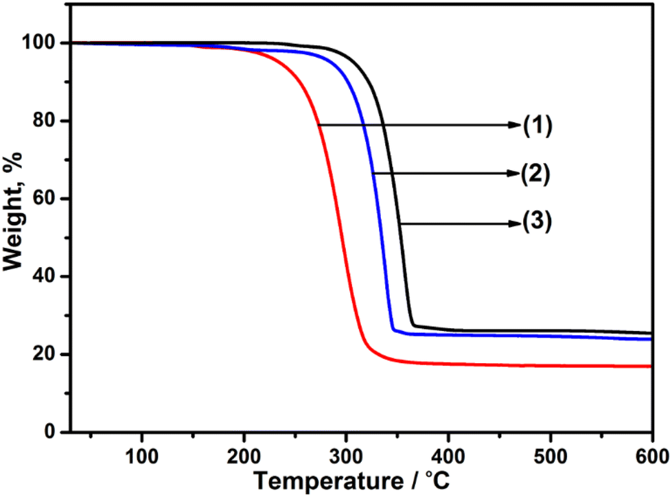 | ||
| Fig. 1 Thermogravimetric analysis (TGA) profiles of (1) [Ga(DTC)3] (expected for Ga2S3: 22.9%), (2) [Cd(DTC)2] (expected for CdS: 25.5%) and (3) [In(DTC)3] (expected for In2S3; 29.1%). | ||
Synthesis of GaxCd1−xS1+0.5x and powder X-ray diffraction analysis
Ga was investigated as a dopant within the CdS lattice. The solid [Ga(DTC)3] precursor was homogeneously mixed as described above with the solid [Cd(DTC)2] precursor. The mixture of [Ga(DTC)3] and [Cd(DTC)2] was then annealed by solventless thermolysis45 to produce GaxCd1−xS1+0.5x. Doping (x) values were selected as 0 (i.e. pure CdS), 0.02, 0.04, 0.06, 0.08 and 0.10 (i.e. 10% dopant). The pXRD patterns of the resultant GaxCd1−xS1+0.5x samples are shown in Fig. 2(a). The pXRD pattern of all samples showed that hexagonal CdS was achieved without any observable impurities of Ga2S3, indicating that Ga has been homogeneously incorporated into the CdS lattice, which was confirmed by further characterisation vide infra. The crystallite sizes of the materials were estimated from the most intense (101) plane using the Scherrer equation.61 Crystallite sizes were found to be 12.9, 16.8, 16.5, 16.7, 18.1 and 16.6 nm for x = 0, 0.02, 0.04, 0.06, 0.08 and 0.10, respectively. Fig. 2(b) reveals the enlarged view of the diffraction peak of the (101) plane for these samples. The 2θmax of the peak slightly shifts to higher 2θ angles with increasing concentration of Ga dopant, in a linear trend with respect to mol% of dopant concentration. This shift may be ascribed to the decrease in unit cell volume (Fig. 2(c)) with the occupation of smaller Ga3+ ions (0.076 nm) replacing the larger Cd2+ (0.109 nm) ions17 in the cationic lattice positions. Consequently, the lattice parameter of CdS was reduced, leading to the reduction of the lattice plane distance (Fig. S4(a) and (b)†). It was observed that d(101) decreases with an increase in 2θ (Fig. S4(c)†). Although this suggests that in this case Ga3+ ions are incorporating substitutionally in the CdS lattice, previous reports have shown that interstitial incorporation can also occur, depending on the synthetic method and dopant concentrations.14,16,17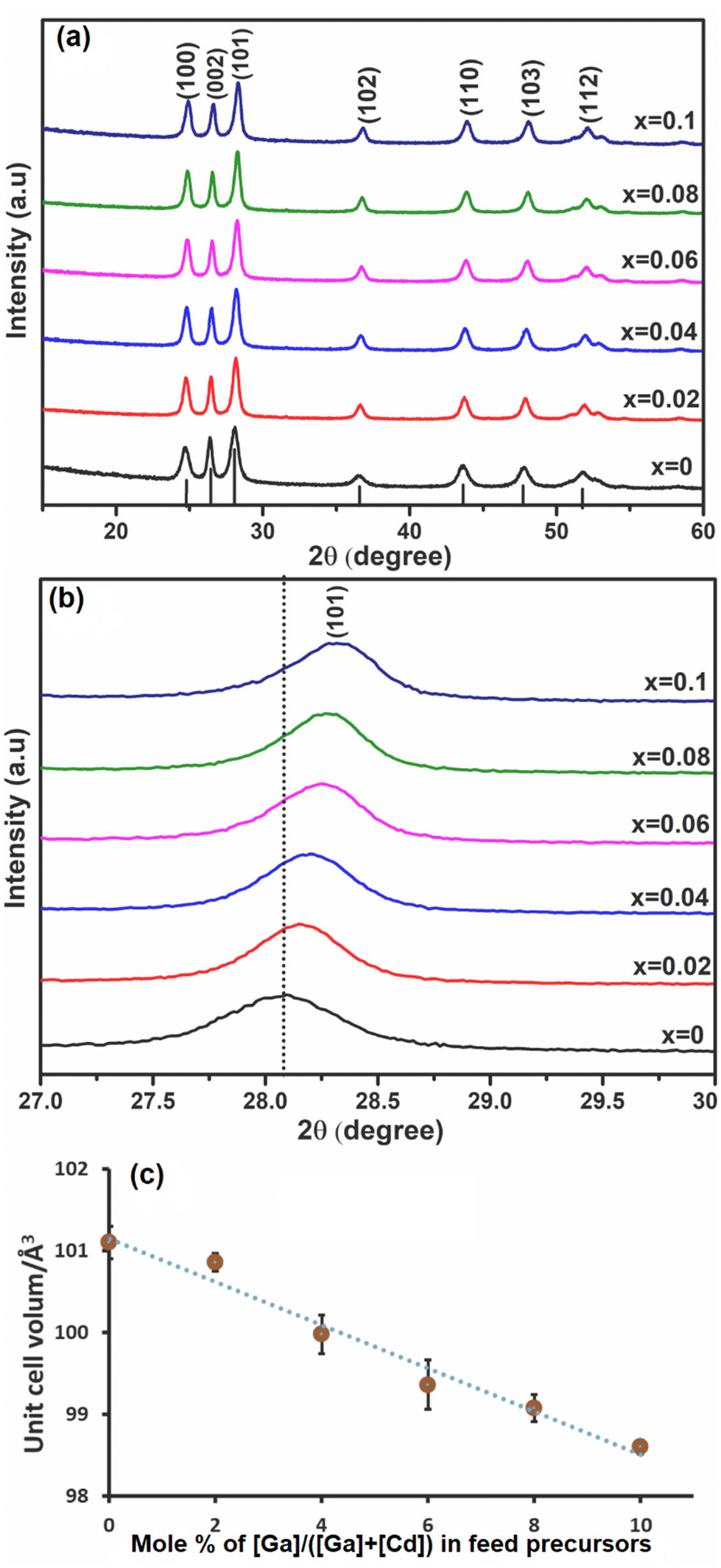 | ||
| Fig. 2 (a) p-XRD patterns of Ga-doped CdS with different mole fractions of GaxCd1−xS1+0.5x, 0 ≤ x ≤ 0.1; (b) an expanded view of (101) plane diffraction for GaxCd1−xS1+0.5x and (c) unit cell volume Å3 of nanoparticles of GaxCd1−xS1+0.5x as a function of Ga mol% where mol% is defined as a % of total metals content i.e. [Ga]/([Cd] + [Ga])%. | ||
Scanning electron microscopy (SEM), energy dispersive X-ray (EDX) spectroscopy and inductively coupled plasma atomic emission (ICP-OES) spectroscopy of GaxCd1−xS1+0.5x
Scanning electron micrographs (Fig. 3) revealed that samples appeared as agglomerated microscale spheres, with no significant morphological changes observable as a function of dopant concentration. We note that microscale-sized particles of Ga-doped CdS have also been observed from materials synthesised by a solvothermal synthesis method.17 Energy-dispersive X-ray (EDX) spectroscopy was also used to assess the homogeneity of Ga throughout the CdS materials. Fig. 4 shows the EDX elemental distribution of Ga, Cd, and S for all doping concentrations. It was found that Ga was homogenously distributed through all materials, which, coupled to the pXRD data above, indicates no observable impurities in the synthesised doped material. Inductively coupled plasma atomic emission (ICP-OES) was also used to quantitatively measure the atomic % of Ga within the systems (Table S3†). Fig. S5† demonstrates that a linear correlation between mol% of [Ga(DTC)3] in the starting mixture and the observed Ga mol% in the products from the thermolysis reaction via both EDX and ICP-OES is observed. These results confirmed the anticipated GaxCd1−xS1+0.5x compositions relative to the stoichiometric amounts of the complexes initially decomposed, again indicating that Ga3+ ions are successfully (and homogeneously) incorporated into the CdS lattice.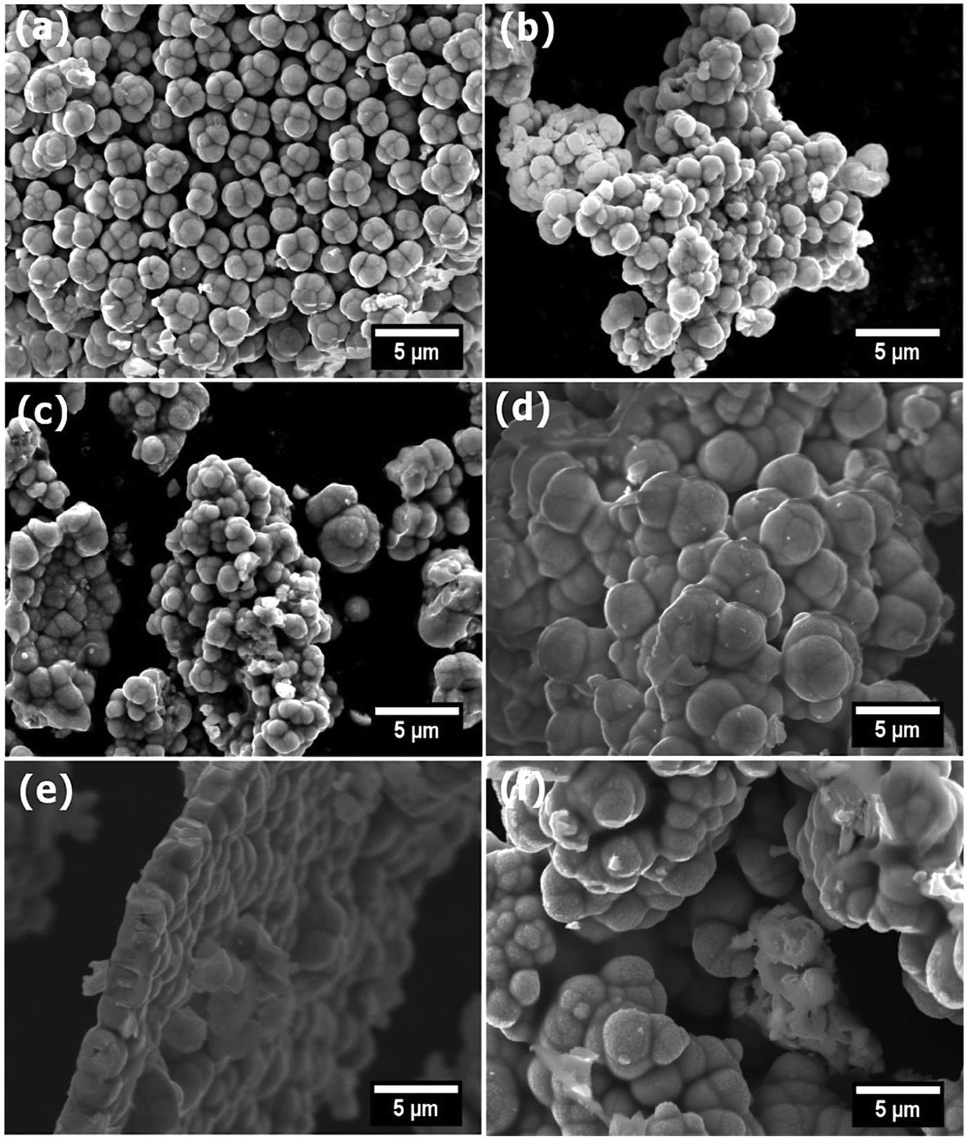 | ||
| Fig. 3 Secondary electron SEM images (10 keV) of doped and undoped samples of GaxCd1−xS1+0.5x, x = 0 (a), x = 0.02 (b), x = 0.04 (c), x = 0.06 (d), x = 0.08 (e) and x = 0.10 (f). | ||
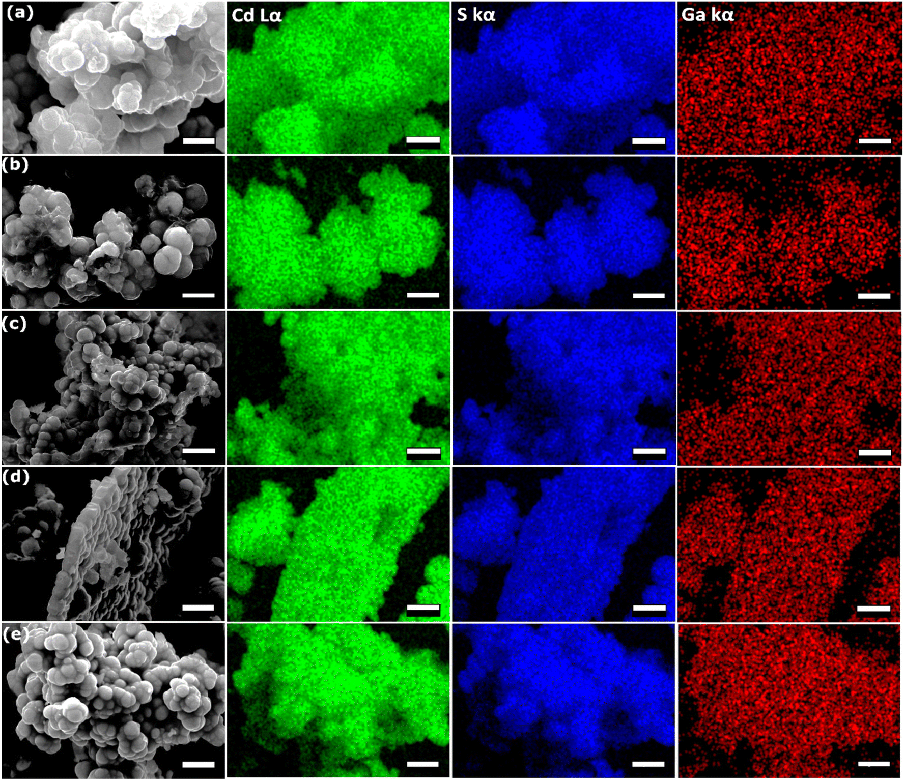 | ||
| Fig. 4 EDX spectroscopic mapping (20 keV) of Cd Lα, Ga Lα and S Kα for GaxCd1−xS1+0.5x samples. (a) x = 0.02, (b) x = 0.04, (c) x = 0.06, (d) x = 0.08 and (e) x = 0.1 mole fractions of gallium. All scale bars correspond to 5 μm. | ||
Synthesis of InxCd1−xS1+0.5x and powder X-ray diffraction (pXRD) analysis
In was next investigated as a dopant in CdS to produce InxCd1−xS1+0.5x, with x = 0, 0.02, 0.04, 0.06, 0.08 and 0.10. The pXRD patterns of InxCd1−xS1+0.5x are shown in Fig. 5(a). For the x = 0.08 and 0.1 systems, crystalline impurities of CdIn2S4![[thin space (1/6-em)]](https://www.rsc.org/images/entities/char_2009.gif) 62 were present (as indicated by the (*) in Fig. 5). No additional peaks were observed in the x = 0.02, 0.04 and 0.06 samples, suggesting that the InxCd1−xS1+0.5x is the major crystalline product from the reaction. From this analysis, it is clear that higher doping levels of In causes impurities, which was not observed with Ga, but is in agreement with a previous report of In-doped CdS.18 From the enlarged view of the (101) reflection (Fig. 5(b)), the crystallite sizes were estimated using the Scherrer equation and were found to be 12.9, 15.4, 14.5, 16.7, 17.7 and 18.8 nm for x = 0, 0.02, 0.04, 0.06, 0.08 and 0.10, respectively. From this further analysis of the (101) plane, it was again observed that the diffraction peak shifts to higher 2θ angles compared to the undoped sample. This shift is lower than for the Ga-doped samples, which is likely due to the larger size of the In3+ cation (0.094 nm), which is closer to the size of Cd2+ (0.109 nm). As a result, the lattice parameter of the CdS was slightly reduced, leading to the reduction of the lattice plane distance (Fig. S6†). It was observed that d(101) decreases slightly from 3.181 to 3.161 Å (Fig. S6†). Furthermore, Fig. 5(c) shows the unit cell volume fluctuating with increasing In doping, this can be attributed to In3+ replacing Cd2+ in the lattice structure.
62 were present (as indicated by the (*) in Fig. 5). No additional peaks were observed in the x = 0.02, 0.04 and 0.06 samples, suggesting that the InxCd1−xS1+0.5x is the major crystalline product from the reaction. From this analysis, it is clear that higher doping levels of In causes impurities, which was not observed with Ga, but is in agreement with a previous report of In-doped CdS.18 From the enlarged view of the (101) reflection (Fig. 5(b)), the crystallite sizes were estimated using the Scherrer equation and were found to be 12.9, 15.4, 14.5, 16.7, 17.7 and 18.8 nm for x = 0, 0.02, 0.04, 0.06, 0.08 and 0.10, respectively. From this further analysis of the (101) plane, it was again observed that the diffraction peak shifts to higher 2θ angles compared to the undoped sample. This shift is lower than for the Ga-doped samples, which is likely due to the larger size of the In3+ cation (0.094 nm), which is closer to the size of Cd2+ (0.109 nm). As a result, the lattice parameter of the CdS was slightly reduced, leading to the reduction of the lattice plane distance (Fig. S6†). It was observed that d(101) decreases slightly from 3.181 to 3.161 Å (Fig. S6†). Furthermore, Fig. 5(c) shows the unit cell volume fluctuating with increasing In doping, this can be attributed to In3+ replacing Cd2+ in the lattice structure.
 | ||
| Fig. 5 (a) pXRD patterns of In-doped CdS with different mole fractions of InxCd1−xS1+0.5x, x = 0, 0.02, 0.04, 0.06, 0.08 and 0.1. Pink stars indicate the presence of minor crystalline impurities of CdIn2S4; (b) expanded region corresponding to the (101) diffraction peak for InxCd1−xS1+0.5x, x = 0, 0.02, 0.04, 0.06, 0.08 and 0.1; (c) unit cell volume (Å3) of InxCd1−xS1+0.5x as a function of In mol% where mol% is defined as a % of total metals content i.e. [In]/([In] + [Cd])%. | ||
Scanning electron microscope (SEM), energy dispersive X-ray (EDX) and inductively coupled plasma atomic emission (ICP-OES) spectroscopies for InxCd1−xS1+0.5x
Representative SEM images of all InxCd1−xS1+0.5x are displayed in Fig. 6. Similar morphologies are observed with the In-doped CdS to the Ga-doped CdS (Fig. 3), with agglomerated microspheres observed for all systems. Analogous to the Ga-doped CdS, the In-doped CdS also showed no significant morphological changes with the increase of indium doping levels up to 6 mol% (Fig. 6). EDX and ICP-OES spectroscopies (Table S4†) were again utilised on the In-doped CdS and again confirmed the expected InxCd1−xS1+0.5x compositions relative to the stoichiometric input [In(DTC)3]. Fig. 7 displays the EDX elemental mapping images of the InxCd1−xS1+0.5x samples, again showing homogeneous distribution of In throughout the CdS materials, in agreement with the pXRD patterns in Fig. 5. As with the Ga-doped CdS samples, the InxCd1−xS1+0.5x systems were found to observe a linear trend of expected In concentration vs. observed In concentration by both EDX and ICP-OES analyses (Fig. S7†).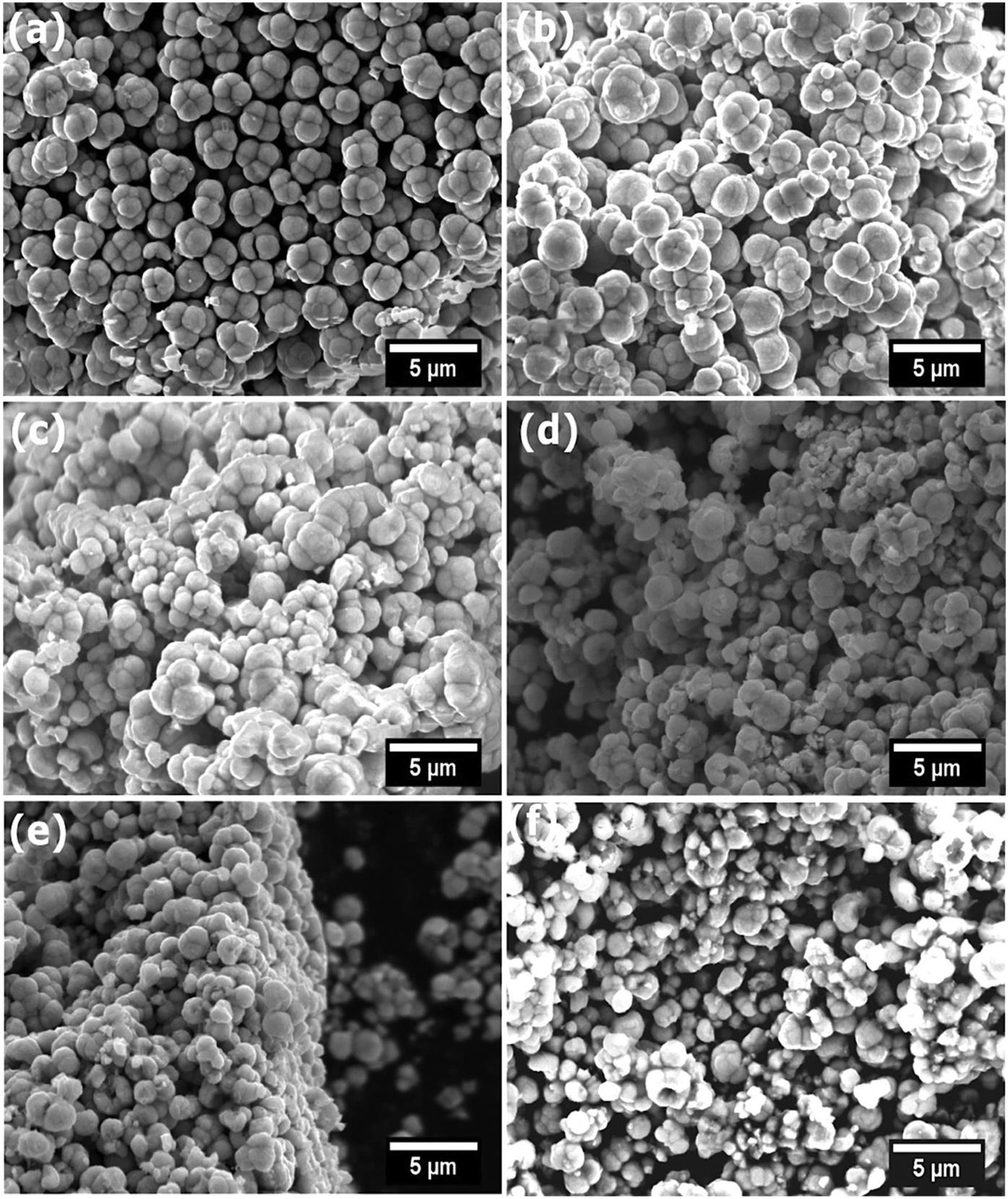 | ||
| Fig. 6 SEM images (10 keV) of doped and undoped samples of InxCd1−xS1+0.5x, x = 0 (a), x = 0.02 (b), x = 0.04 (c), x = 0.06 (d), x = 0.08 (e) and x = 0.10 (f). | ||
 | ||
| Fig. 7 EDX spectroscopic mapping (20 keV) of Cd Lα, In Lα and S Kα for InxCd1−xS1+0.5x samples. (a) x = 0.02, (b) x = 0.04, (c) x = 0.06, (d) x = 0.08 and (e) x = 0.1 mole fractions of gallium. All scale bars correspond to 5 μm. | ||
Raman spectroscopy of MxCd1−xS1+0.5x (M = Ga/In)
Raman spectroscopy was used to investigate all Ga- and In-doped CdS samples. Fig. 8 shows the obtained Raman spectra of all investigated samples, which all confirm hexagonal CdS was achieved for all samples.54,55 CdS has two main longitudinal optical (LO) bands centred ca. 297.39 cm−1 and 597.19 cm−1, which correspond to 1LO and 2LO for hexagonal CdS.5,41,63,64 The broad intense peak of 1LO is slightly shifted towards shorter wavelength compared to the literature (in both Ga- and In-doped samples), which may be due to the grain-size effect.26 No change was observed in the Raman spectra for the doped samples, indicative of the CdS maintaining its parent phase purity,14,65 despite the presence of a minor CdIn2S4 impurity as observed in the pXRD analysis.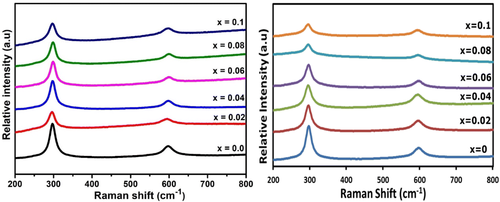 | ||
| Fig. 8 Raman spectra of (lhs) GaxCd1−xS1+0.5x, where x = 0, 0.02, 0.04, 0.06, 0.08 and 0.1 and (rhs) InxCd1−xS1+0.5x, where x = 0, 0.02, 0.04, 0.06, 0.08 and 0.1. | ||
UV-Vis spectroscopy and photoluminescence (PL) of MxCd1−xS1+0.5x (M = Ga and In)
The optical attenuation properties of these samples were measured by UV-Vis spectroscopy from a dispersion of the particulate material in DMSO (Fig. S8 and S9†). The optical attenuation through each sample was broadly constant across the visible part of the spectrum before rising strongly in the UV. The approximately constant optical attenuation in the visible, despite this region encompassing the likely absorption edge for the material (for bulk CdS, the band gap is 2.4 eV i.e. 520 nm), suggests that scattering dominates over absorption at these wavelengths. Photoluminescence (PL) analysis was thus used instead to assess the band gap of these materials.Fig. 9(a) shows PL spectra for the undoped and doped GaxCd1−xS1+0.5x samples obtained using an excitation wavelength of 350 nm at room temperature. Two broad bands are evident, similar to the blue and green bands previously observed in Cu-doped CdS thin films22 and nanoparticles66 as well as Fe-doped CdS nanorods.67 A sharp excitation-dependent peak at 390 nm is also observed in the PL spectra, which has been identified as the first-order Raman scattering from the DMSO solvent.68 The blue band emission has been attributed to the excitonic emission of CdS, which corresponds to a band gap energy of ∼2.7–2.9 eV, similar to those reported by Mandal et al.66 CdS nanomaterials like these, are often found to possess band gap energies higher than those reported for bulk CdS (2.4 eV), depending on their size and shape due to strain, surface effects, or quantum confinement (CdS exciton Bohr radius = 5.8 nm).69–71 On the other hand, the green band emission has been attributed to deep surface defect trap states16 (Cd and S vacancies69). The relative intensities of these bands can be increased and decreased depending on the concentration of dopants.22,67 In this case, undoped CdS shows only the blue band emission (suggesting a low density of surface defects in the undoped sample) with two broad features centred at 411 nm and 436 nm, with similar intensities, as well as a shoulder at 463 nm. As the Ga doping concentration is increased, the intensity of the shoulder increases, matching the intensity of the other two features for samples with 2%, 4% and 6% Ga and becoming the most intense feature for samples with 8% and 10% Ga. More noticeably, the green band (centred at 524 nm) emerges in the spectra as the Ga doping percentage is increased, until it almost matches the intensity of the blue band at 4% doping concentration. This is accompanied by an overall increase in PL intensity as the Ga concentration is increased where the blue band is slightly more intense than the green band in all cases. These observations suggest that introducing Ga dopants into the CdS structure has an effect both in the blue and green band emission of the samples. In the blue band, substitution of Cd ions by Ga appears to modify the near band extended states, acting as a shallow donor and red-shifting the emission. Additionally, it has been shown that introducing dopants such as Ga and Al14 in the CdS lattice causes a decrease in surface sulfur, introducing surface defect states that are responsible for the green band emission.16
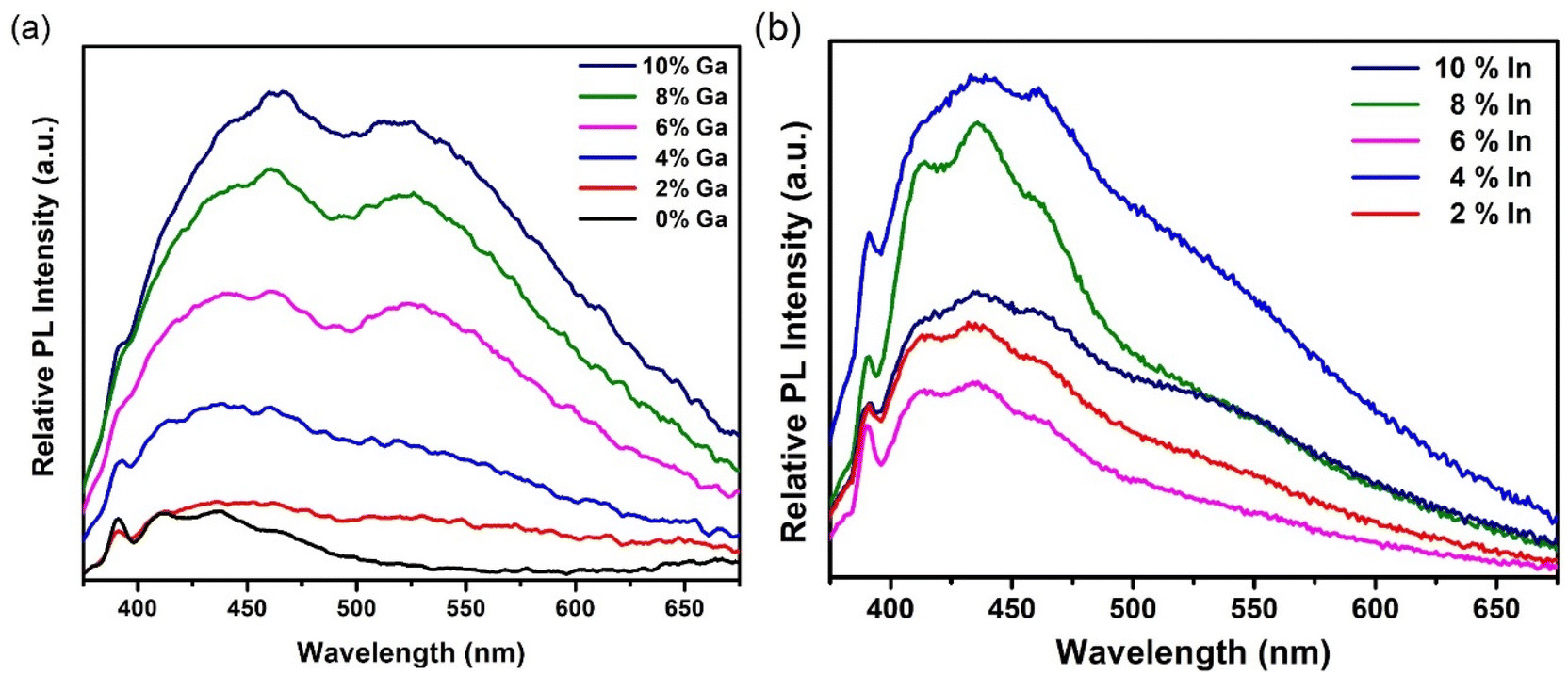 | ||
| Fig. 9 (a) PL spectra of undoped and Ga-doped CdS nanoparticles (b) PL spectra of In-doped CdS nanoparticles at an excitation wavelength of 350 nm. | ||
Room temperature PL spectra of indium-doped samples were also obtained using an excitation wavelength of 350 nm, as shown in Fig. 9(b). In this case, the blue band with its three previously described features (centred at 411 nm, 436 nm, and 463 nm) is significantly more prominent than the green band, which appears only as a shoulder for all indium doping levels. This suggests that in contrast to Ga3+, In3+ mainly affects the excitonic emission at the band edge without introducing a significant amount of surface defects, maybe because its ionic radius is closer to that of Cd2+.
The recombination dynamics of the blue and green bands in the PL emission were further investigated by analysing the PL decays obtained from Time-Correlated Single-Photon Counting (TCSPC) experiments as shown in Fig. 10, for the undoped samples as well as for those doped with 4% and 10% of Ga and In. It can be seen in Fig. 10 that in all cases, the PL decay is faster for the undoped sample than for doped samples. These were fitted by global bi-exponential decay equations of the form:
| IPL = y0 + A1e−t/τ1 + A2e−t/τ2, | (1) |
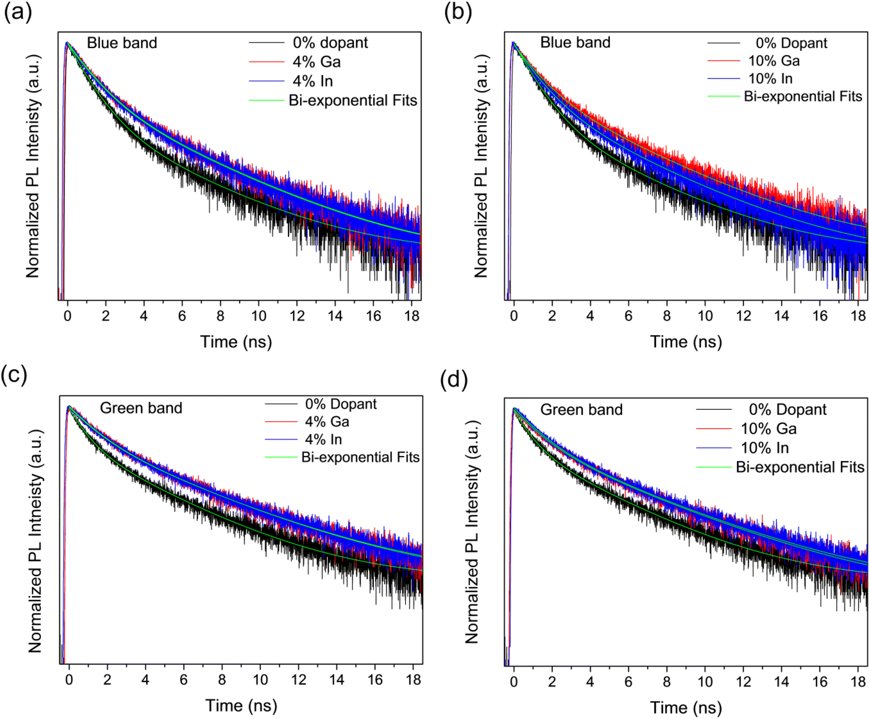 | ||
| Fig. 10 PL decays recorded at the wavelengths corresponding to the blue band for (a) 4, (b) and the green band for (c) 4 and (d) 10 mol% dopant concentrations all compared to the undoped sample. The fit to the bi-exponential decay equation is also shown. | ||
We note here that the doping element makes no significant difference to the lifetimes within the resolution limit of the experiment and that the measured lifetimes are in agreement with those previously reported for other CdS structures.72 Further increasing the dopant concentration to 10% does not increase the lifetimes further, but modifies the fractional amplitudes associated to these same time constants. This variation in amplitude with doping element is only significant at the maximum doping concentration studied here (10%).
The changes in lifetimes and associated amplitudes observed for the decays of the blue and green band emissions are summarized and shown graphically in Fig. S10.† As can be seen in the figure, the time constants for the blue band are approximately constant with doping whilst for the green band there is a modest increase in the time constants between the undoped and doped samples. Conversely, there is no clear trend with doping for the amplitude coefficients in the green band, but a decrease in A1 and increase in A2 with doping in the blue band. Although the blue band is broadly associated with excitonic recombination and the green with defect recombination, which increases with doping, there is evidently significant overlap between them and so PL transients measured across the spectrum will have components associated with both types of process. This makes identification of components with either process difficult,72 however, the change in A1 and A2 with doping for the blue band suggests the shortest time component is associated with excitonic recombination and the longest with defect recombination. Currently, fast recombination rates of photo-excited species is one of the significant limitation in photoelectrocatalysis.13,73–75 Overall, the modest increase in PL lifetime with doping indicates a corresponding improvement in the lifetime of photogenerated electrons and holes, which will benefit the photocatalytic activity.
Conclusions
The Ga and In-doped CdS and pure CdS materials were synthesised by solventless thermolysis from diethyldithiocarbamate precursors. The powder X-ray diffraction patterns of the doped and undoped samples confirmed that it produces a hexagonal CdS and that both Ga and In can be successfully incorporated into the CdS lattice without producing any impurities for all Ga doping concentrations (up to 10 mol%) and In up to 6 mol%. EDX and ICP-OES spectroscopies confirmed the presence of Ga- and In-dopant ions in the CdS matrix. SEM images of the particulate products show microscale agglomerates of spherical nanoparticles. The Raman spectra showed that the 1LO and 2LO peaks of the Ga and In-doped CdS nanoparticles were not shifted to higher or lower wavenumbers when compared to CdS. Photoluminescence measurements of the samples showed that an apparent band gap of these materials is ca. 2.7–2.8 eV. Moderate doping seems to slow down recombination by increasing the lifetimes of excitonic and surface state emissions, but particularly for the latter, demonstrating enhanced charge carrier lifetime and that these doped materials are therefore excellent candidates for enhanced photocatalysis. We have therefore demonstrated that the use of solventless thermolysis of single source precursors is a facile, simple, rapid, and low temperature approach towards doped GaxCd1−xS1+0.5x and InxCd1−xS1+0.5x, which could easily be extended to other dopant metals and parent metal sulfide materials due to the vast library of available precursors from transition, main group, and lanthanide metals.Conflicts of interest
There are no conflicts of interest to declare.Acknowledgements
S. Alderhami would like to acknowledge the Royal Embassy Saudi Arabia Culture Bureau London and Al-Baha University for financial support. SA would also like to thank Dr Siphamandla C Masikane at School of Chemistry, University of Zululand, for helpful discussions. DJL would like to acknowledge EPSRC grant EP/R022518/1.References
- M. Afzaal and P. O'Brien, J. Mater. Chem., 2006, 16, 1597–1602 RSC.
- P. O'Brien and J. McAleese, J. Mater. Chem., 1998, 8, 2309–2314 RSC.
- H. C. Leventis, S. P. King, A. Sudlow, M. S. Hill, K. C. Molloy and S. A. Haque, Nano Lett., 2010, 10, 1253–1258 CrossRef CAS PubMed.
- S. G. Kumar and K. S. R. K. Rao, Energy Environ. Sci., 2014, 7, 45–102 RSC.
- M. A. Buckingham, A. L. Catherall, M. S. Hill, A. L. Johnson and J. D. Parish, Cryst. Growth Des., 2017, 17, 907 CrossRef CAS.
- T. Trindade, P. O'Brien and N. L. Pickett, Chem. Mater., 2001, 13, 3843–3858 CrossRef CAS.
- M. F. Kuehnel, D. W. Wakerley, K. L. Orchard and E. Reisner, Angew. Chem., Int. Ed., 2015, 54, 9627–9631 CrossRef CAS PubMed.
- M. F. Kuehnel, K. L. Orchard, K. E. Dalle and E. Reisner, J. Am. Chem. Soc., 2017, 139, 7217–7223 CrossRef CAS PubMed.
- D. W. Wakerley, M. F. Kuehnel, K. L. Orchard, K. H. Ly, T. E. Rosser and E. Reisner, Nat. Energy, 2017, 2, 1–9 Search PubMed.
- L. M. Peter, Philos. Trans. R. Soc., A, 2011, 369, 1840–1856 CrossRef CAS PubMed.
- Z. B. K. Gutierrez, P. G. Zayas-Bazán, O. de Melo, F. de Moure-Flores, J. A. Andraca-Adame, L. A. Moreno-Ruiz, H. Martínez-Gutiérrez, S. Gallardo, J. Sastré-Hernández and G. Contreras-Puente, Materials, 2018, 11, 2–9 Search PubMed.
- X. Ning and G. Lu, Nanoscale, 2020, 12, 1213–1223 RSC.
- T. Simon, M. T. Carlson, J. K. Stolarczyk and J. Feldmann, ACS Energy Lett., 2016, 1, 1137–1142 CrossRef CAS.
- H. Khallaf, G. Chai, O. Lupan, L. Chow, S. Park and A. Schulte, Appl. Surf. Sci., 2009, 255, 4129–4134 CrossRef CAS.
- H. Khallaf, G. Chai, O. Lupan, L. Chow, H. Heinrich, S. Park and A. Schulte, Phys. Status Solidi A, 2009, 206, 256–262 CrossRef CAS.
- S. Yılmaz, I. Polat, M. A. Olgar, M. Tomakin, S. B. Töreli and E. Bacaksız, J. Mater. Sci.: Mater. Electron., 2017, 28, 3191–3199 CrossRef.
- J. Yang, R. Liu, S. Huang, Y. Shao, Y. Huang and Y. Yu, Catal. Today, 2014, 224, 104–113 CrossRef CAS.
- A. M. Abdulkarem, E. M. Elssfah, N. N. Yan, G. Demissie and Y. Yu, J. Phys. Chem. Solids, 2013, 74, 647–652 CrossRef CAS.
- Y. Chen, F. Wang, H. Xu, S. Ren, H. Gu, L. Wu, W. Wang and L. Feng, Chalcogenide Lett., 2017, 14, 1–9 Search PubMed.
- C. Barglik-Chory, C. Remenyi, C. Dem, M. Schmitt, W. Kiefer, C. Gould, C. Rüster, G. Schmidt, D. M. Hofmann, D. Pfisterer and G. Müller, Phys. Chem. Chem. Phys., 2003, 5, 1639–1643 RSC.
- S. Chandramohan, A. Kanjilal, S. N. Sarangi, S. Majumder, R. Sathyamoorthy, C.-H. Hong and T. Som, Nanoscale, 2010, 2, 1155 RSC.
- M. Muthusamy and S. Muthukumaran, Optik, 2015, 126, 5200–5206 CrossRef CAS.
- A. Nazir, A. Toma, N. A. Shah, S. Panaro, S. Butt, R. U. R. Sagar, W. Raja, K. Rasool and A. Maqsood, J. Alloys Compd., 2014, 609, 40–45 CrossRef CAS.
- Z. D. Eygi, B. Demirselük and V. Bilgin, Int. J. Thin Film Sci. Technol., 2016, 5, 103–106 CrossRef PubMed.
- S. Yılmaz, I. Polat, M. Tomakin, T. Küçükömeroğlu, S. B. Töreli and E. Bacaksız, Appl. Phys. A: Mater. Sci. Process., 2018, 124, 1–8 CrossRef.
- M. Thambidurai, N. Muthukumarasamy, D. Velauthapillai and C. Lee, J. Mater. Sci.: Mater. Electron., 2013, 24, 4535–4541 CrossRef CAS.
- S. Yılmaz, I. Polat, M. Tomakin, S. B. Töreli, T. Küçükömeroğlu and E. Bacaksız, J. Mater. Sci.: Mater. Electron., 2018, 29, 14774–14782 CrossRef.
- Z. Q. Qin and F. J. Zhang, Appl. Surf. Sci., 2013, 285, 912–917 CrossRef CAS.
- V. Narasimman, V. S. Nagarethinam, K. Usharani and A. R. Balu, Optik, 2017, 138, 398–406 CrossRef CAS.
- C. Guo, K. Tian, L. Wang, F. Liang, F. Wang, D. Chen, J. Ning, Y. Zhong and Y. Hu, J. Colloid Interface Sci., 2021, 583, 661–671 CrossRef CAS PubMed.
- Y. Wang, J. Wu, J. Zheng, R. Jiang and R. Xu, Catal. Sci. Technol., 2012, 2, 581–588 RSC.
- S. Butt, N. A. Shah, A. Nazir, Z. Ali and A. Maqsood, J. Alloys Compd., 2014, 587, 582–587 CrossRef CAS.
- C. Wu, C. Jiang, X. Wang, H. Ding, H. Ju, L. Zhang, T. Chen and C. Zhu, ACS Appl. Mater. Interfaces, 2019, 11, 3207–3213 CrossRef CAS PubMed.
- S. Alhammadi, H. Jung, S. Kwon, H. Park, J. J. Shim, M. H. Cho, M. Lee, J. S. Kim and W. K. Kim, Thin Solid Films, 2018, 660, 207–212 CrossRef CAS.
- H. Luo, C. Tuinenga, E. B. Guidez, C. Lewis, J. Shipman, S. Roy, C. M. Aikens and V. Chikan, J. Phys. Chem. C, 2015, 119, 10749–10757 CrossRef CAS.
- S. Roy, C. Tuinenga, F. Fungura, P. Dagtepe, V. Chikan and J. Jasinski, J. Phys. Chem. C, 2009, 113, 13008–13015 CrossRef CAS.
- C. Tuinenga, J. Jasinski, T. Iwamoto and V. Chikan, ACS Nano, 2008, 2, 1411–1421 CrossRef CAS PubMed.
- M. Nawaz, S. Akhtar, F. Qureshi, S. A. Almofty and V. Nissapatron, J. Mol. Struct., 2022, 1253, 132288 CrossRef CAS.
- R. Sasikala, A. R. Shirole, V. Sudarsan, K. G. Girija, R. Rao, C. Sudakar and S. R. Bharadwaj, J. Mater. Chem., 2011, 21, 16566–16573 RSC.
- V. Bala, S. K. Tripathi and R. Kumar, Mater. Lett., 2015, 149, 18–21 CrossRef CAS.
- M. A. Buckingham, K. Norton, P. D. McNaughter, G. Whitehead, I. Vitorica-Yrezabal, F. Alam, K. Laws and D. J. Lewis, Inorg. Chem., 2022, 61, 8206–8216 CrossRef CAS PubMed.
- J. C. Sarker and G. Hogarth, Chem. Rev., 2020, 121, 6057–6123 CrossRef PubMed.
- N. Zeng, D. G. Hopkinson, B. F. Spencer, S. G. McAdams, A. A. Tedstone, S. J. Haigh and D. J. Lewis, Chem. Commun., 2019, 55, 99–102 RSC.
- T. Alqahtani, R. J. Cernik, P. O'Brien and D. J. Lewis, J. Mater. Chem. C, 2019, 7, 5112–5121 RSC.
- F. Makin, F. Alam, M. A. Buckingham and D. J. Lewis, Sci. Rep., 2022, 12, 5627 CrossRef CAS PubMed.
- A. A. Tedstone, E. A. Lewis, N. Savjani, X. L. Zhong, S. J. Haigh, P. O'Brien and D. J. Lewis, Chem. Mater., 2017, 29, 3858–3862 CrossRef CAS.
- Y. T. Alharbi, F. Alam, K. Parvez, M. Missous and D. J. Lewis, Inorg. Chem., 2021, 60, 13691–13698 CrossRef CAS.
- K. Norton, J. Jacobs, J. Neilson, D. Hopkinson, M. Z. Mokhtar, R. J. Curry and D. J. Lewis, RSC Adv., 2021, 11, 26813–26819 RSC.
- Y. T. Alharbi, F. Alam, A. Salhi, M. Missous and D. J. Lewis, Sci. Rep., 2021, 11, 1–8 CrossRef PubMed.
- E. P. C. Higgins, S. G. McAdams, D. G. Hopkinson, C. Byrne, A. S. Walton, D. J. Lewis and R. A. W. Dryfe, Chem. Mater., 2019, 31, 5384–5391 CrossRef CAS.
- A. Elgendy, A. A. Papaderakis, C. Byrne, Z. Sun, J. V. Lauritsen, E. P. C. Higgins, A. Ejigu, R. Cernik, A. S. Walton, D. J. Lewis and R. A. W. Dryfe, ACS Appl. Energy Mater., 2021, 4, 13015–13026 CrossRef CAS.
- K. Norton, J. Kunstmann, L. Ping, A. Rakowski, C. Wang, A. J. Marsden, G. Murtaza, N. Zeng, S. J. McAdams, M. A. Bissett, S. J. Haigh, B. Derby, G. Seifert and D. J. Lewis, Chem. Sci., 2019, 10, 1035–1045 RSC.
- M. Al-Shakban, P. D. Matthews, X. L. Zhong, I. Vitorica-Yrezabal, J. Raftery, D. J. Lewis and P. O'Brien, Dalton Trans., 2018, 47, 5304–5309 RSC.
- S. Shen, Y. Zhang, L. Peng, B. Xu, Y. Du, M. Deng, H. Xu and Q. Wang, CrystEngComm, 2011, 13, 4572–4579 RSC.
- G. Murtaza, S. Alderhami, Y. T. Alharbi, U. Zul, M. Hossin, A. M. Alanazi, L. Almanqur, E. U. Onche, S. P. Venkateswaran and D. J. Lewis, ACS Appl. Energy Mater., 2020, 3, 1952–1961 CrossRef CAS PubMed.
- M. Edler, T. Rath, A. Schenk, A. Fischereder, W. Haas, M. Edler, B. Chernev, B. Kunert, F. Hofer, R. Resel and G. Trimmel, Mater. Chem. Phys., 2012, 136, 582–588 CrossRef CAS.
- D. P. Dutta, V. K. Jain, A. Knoedler and W. Kaim, Polyhedron, 2002, 21, 239–246 CrossRef CAS.
- W.-S. Jung, C. S. Ra and B.-K. Min, Bull. Korean Chem. Soc., 2005, 26, 131–135 CrossRef CAS.
- R. Nomura, S. Inazawa, K. Kanaya and H. Matsuda, Appl. Organomet. Chem., 1989, 3, 195–197 CrossRef CAS.
- R. Marx Nirmal, K. Pandian and K. Sivakumar, Appl. Surf. Sci., 2011, 257, 2745–2751 CrossRef CAS.
- S. M. Kumaran and R. Gopalakrishnan, J. Sol-Gel Sci. Technol., 2012, 62, 193–200 CrossRef.
- J. Peng, Z. Zheng, H. Tan, J. Yang, D. Zheng, Y. Song, F. Lu, Y. Chen and W. Gao, Sens. Actuators, B, 2022, 363, 131863 CrossRef CAS.
- A. Pan, R. Liu, Q. Yang, Y. Zhu, G. Yang, B. Zou and K. Chen, J. Phys. Chem. B, 2005, 109, 24268–24272 CrossRef CAS PubMed.
- V. Singh, P. K. Sharma and P. Chauhan, Mater. Chem. Phys., 2010, 121, 202–207 CrossRef CAS.
- G. Perna, V. Capozzi, M. Ambrico, V. Augelli, T. Ligonzo, A. Minafra, L. Schiavulli and M. Pallara, Thin Solid Films, 2004, 453–454, 187–194 CrossRef CAS.
- P. Mandal, S. S. Talwar, S. S. Major and R. S. Srinivasa, J. Chem. Phys., 2008, 128, 114703 CrossRef CAS PubMed.
- K. Kaur, G. S. Lotey and N. K. Verma, J. Mater. Sci.: Mater. Electron., 2014, 25, 2605–2610 CrossRef CAS.
- M. E. Wankhede and S. K. Haram, Chem. Mater., 2003, 15, 1296–1301 CrossRef CAS.
- J. Su, T. Zhang, Y. Li, Y. Chen and M. Liu, Molecules, 2016, 21, 735 CrossRef PubMed.
- P. Thangadurai, S. Balaji and P. T. Manoharan, Nanotechnology, 2008, 19, 435708 CrossRef CAS PubMed.
- M. Thambidurai, N. Muthukumarasamy, S. Agilan, N. Murugan, S. Vasantha, R. Balasundaraprabhu and T. S. Senthil, J. Mater. Sci., 2010, 45, 3254–3258 CrossRef CAS.
- F. Wu, J. Z. Zhang, R. Kho and R. K. Mehra, Chem. Phys. Lett., 2000, 330, 237–242 CrossRef CAS.
- K. Wu, Z. Chen, H. Lv, H. Zhu, C. L. Hill and T. Lian, J. Am. Chem. Soc., 2014, 136, 7708–7716 CrossRef CAS PubMed.
- K. Wu, Y. Du, H. Tang, Z. Chen and T. Lian, J. Am. Chem. Soc., 2015, 137, 10224–10230 CrossRef CAS PubMed.
- M. J. Berr, P. Wagner, S. Fischbach, A. Vaneski, J. Schneider, A. S. Susha, A. L. Rogach, F. Jäckel and J. Feldmann, Appl. Phys. Lett., 2012, 100, 223903 CrossRef.
Footnote |
| † Electronic supplementary information (ESI) available. See DOI: https://doi.org/10.1039/d3dt00239j |
| This journal is © The Royal Society of Chemistry 2023 |