
Orienting and shaping organic semiconductor single crystals through selective nanoconfinement
Aida
Alaei
 a,
Kai
Zong
a,
Kaustubh
Asawa
b,
Tseng-Ming
Chou
a,
Alejandro L.
Briseño
c,
Chang-Hwan
Choi
b and
Stephanie S.
Lee†
*a
a,
Kai
Zong
a,
Kaustubh
Asawa
b,
Tseng-Ming
Chou
a,
Alejandro L.
Briseño
c,
Chang-Hwan
Choi
b and
Stephanie S.
Lee†
*a
aDepartment of Chemical Engineering and Materials Science, Stevens Institute of Technology, Hoboken, NJ 07030, USA
bDepartment of Mechanical Engineering, Stevens Institute of Technology, Hoboken, NJ 07030, USA
cDepartment of Chemistry, Pennsylvania State University, University Park, PA 16802, USA
First published on 26th December 2020
Abstract
For organic semiconductor crystals exhibiting anisotropic charge transport along different crystallographic directions, nanoconfinement is a powerful strategy to control crystal orientation by aligning the fast crystallographic growth direction(s) with the unconfined axis(es) of nanoconfining scaffolds. Here, design rules are presented to relate crystal morphology, scaffold geometry, and orientation control in solution-processed small-molecule crystals. Specifically, organic semiconductor triisopropylsilylethynyl pyranthrene needle-like crystals with a dimensionality of n = 1 and perylene platelike crystals with n = 2 were grown from solution within nanoconfining scaffolds comprising cylindrical nanopores with a dimensionality of m = 1, representing one unconfined dimension along the cylinder axis, and those comprising nanopillar arrays with a dimensionality of m = 2. For m = n systems, native crystal growth habits were preserved while the crystal orientation in n = m direction(s) was dictated by the geometry of the scaffold. For n ≠ m systems, on the other hand, orientation control was restricted within a single plane, either parallel or perpendicular to the substrate surface. Intriguingly, control over crystal shape was also observed for perylene crystals grown in cylindrical nanopores (n > m). Within the nanopores, crystal growth was restricted along a single direction to form a needle-like morphology. Once growth proceeded above the scaffold surface, the crystals adopted their native growth habit to form asymmetric T-shaped single crystals with concave corners. These findings suggest that nanoporous scaffolds with spatially-varying dimensionalities can be used to grow single crystals of complex shapes.
Introduction
In the field of organic electronics, controlling the orientation of organic semiconductor crystals, particularly during rapid solution processing to drive down fabrication costs, remains an outstanding challenge. In these materials, delocalized π-orbitals allow charges to hop from one molecule to the next. Because the extent of π-orbital overlap, or more specifically the magnitude of the intermolecular charge transfer integral,1 varies with crystallographic direction, organic semiconductor crystals exhibit charge transport anisotropy. In the seminal work of Sundar, Zaumseil, Podzorov and coworkers, hole mobilities in a single rubrene crystal were observed to vary by a factor of 3.5 depending on the crystal orientation with respect to co-planar source and drain electrodes.2 Controlling the crystal orientation with respect to the electrode configuration is thus critical for obtaining optimal device performance.Over the past two decades, significant progress has been made in controlling the in-plane orientation of crystals in solution-processed organic semiconductor thin films through the use of external forces, such as solution shearing3–5 and electric fields.6,7 Controlling the out-of-plane orientation of organic semiconductor crystals during solution phase processing has proven much more difficult. Coating underlying substrates with graphene to induce a face-on orientation of conjugated molecules such that their π-planes are parallel to the substrate surface has been successfully demonstrated for several thermally-evaporated compounds, including pentacene8–10 and pthalocyanines.9,11–13 For solution-processed compounds, this strategy has been employed to grow vertical crystals of aniline oligomers.14 For most solution-processable compounds, however, the presence of bulky side groups that impart solubility to the conjugated molecules typically prevent significant interactions between their π-planes and those of graphene.15
To this end, nanoconfinement on the tens to hundreds of nanometer length scale is a promising strategy to control the orientation of molecular crystals. Because organic molecules are generally asymmetric, crystal growth occurs at different rates along different crystallographic directions. In nanoconfined spaces, the fast growth direction of crystals tends to align with the unconfined direction of the nanoconfining space, for example the long axis of cylindrical nanopores.16,17 Over the past decade, preferred orientation of organic semiconductor wires within nanogrooves18–21 and nanocylinders11,22 has been demonstrated for several solution-processed systems. Recently, our group has demonstrated the use of nanoconfining scaffolds to form vertical crystal arrays of small-molecule organic semiconductors triisopropylsilylethynyl pyranthrene and perylene through a continuous solution dip-coating process. When needle-like TIPS-PY crystals were grown from solution in the cylindrical nanopores of anodized aluminium oxide (AAO) scaffolds, the long axis of the needles aligned with the long axis of the pores.23 Significantly, crystal growth proceeded above the scaffold surfaces to form high-surface area vertical crystal arrays. For perylene crystals deposited from solution onto lithographically-patterned Si nanopillar scaffolds, these platelike crystals were likewise found to orient with the flat faces perpendicular to the substrate surface.24 For both of these systems, the fast charge transport direction of the crystals was oriented perpendicular to the substrate surface, ideal for sandwich electrode configurations used in organic solar cells and light-emitting diodes.
In the above studies, the nanoconfining scaffolds were selected based on the crystal growth habit of the small-molecule organic semiconductor. Namely, needle-like TIPS-PY crystals with one long axis were grown in cylindrical nanopores that also have one long axis. In contrast, platelike perylene crystals with two long axes were grown in nanopillar scaffolds, with two unconfined growth directions parallel and perpendicular to the substrate surface. Here we ask the question of how scaffold-directed crystal growth proceeds when the crystal growth habit is not matched with the scaffold geometry. By exploring different combinations of crystal growth habits and nanoconfining scaffold geometries comprising nanopore and nanopillar arrays, we elucidate the role of such scaffolds in dictating the orientation and shape of organic semiconductor crystals.
Results and discussion
To examine the role of scaffold dimensionality in directing the solution-phase crystallization of small-molecule organic semiconductors, we examined the crystal growth of two compounds, TIPS-PY and perylene, in two scaffold geometries comprising either nanopillar or nanopore arrays. Fig. 1A displays a TIPS-PY crystal grown from solution. TIPS-PY adopts a needle-like morphology with fast growth along the π-stack direction,23 as displayed in the schematic. Since growth occurs fastest along a single crystallographic direction, the dimensionality of the crystal was assigned as n = 1. In contrast, perylene crystals grown from solution adopt a platelike morphology with fast growth along two crystallographic directions, as indicated by the red arrows in Fig. 1B. The dimensionality of perylene crystals was assigned as n = 2. Previous X-ray diffraction measurements confirmed that perylene adopts the α-phase.24 This phase is also evident by the 92° corners of the perylene crystals. For comparison, β-perylene crystals adopt a rhombohedral shape with corner angles of 122° and 58°.25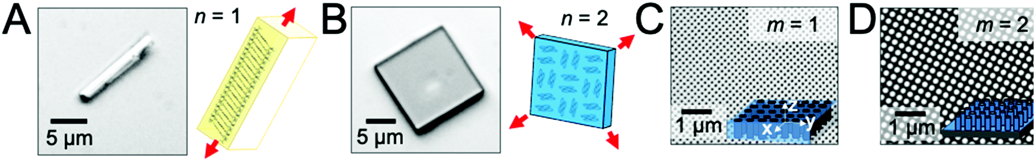 | ||
| Fig. 1 Optical micrographs of (A) a needle-like TIPS-PY crystal with n = 1 and (B) a platelike perylene crystal with n = 2 grown from solution on flat SiO2 substrates. Schematics illustrate the molecular orientation relative to the crystal shape, with fast growth directions highlighted by red arrows. Scanning electron microscope (SEM) images of lithographically-defined silicon scaffolds comprising (C) cylindrical nanopores with m = 1 and (D) cylindrical nanopillars with m = 2. 3D illustrations of the scaffolds are provided as insets for clarity. Reference axes are provided in the inset in (C). | ||
Fig. 1C displays the scanning electron microscopy (SEM) images of silicon scaffolds comprising cylindrical nanopores defined by holographic lithography. The dimensionality can be characterized by m = 1, representing one unconfined direction along the long axis of the cylindrical pores (i.e. the z direction). For nanopillar grids, on the other hand, unconfined growth can occur both parallel to the substrate surface, along either the rows or columns between nanopillars in the x or y direction, and perpendicular to the substrate surface along the z direction (Fig. 1D). A dimensionality of m = 2 was assigned for these scaffolds. The average nanopillar height was measured by cross-sectional SEM to be ∼600 nm.
Scaffolds with m = 2
To determine the role of scaffold dimensionality in directing small molecule crystallization, we first examined crystal growth in m = 2 scaffolds, i.e. nanopillar arrays. Fig. 2A and B display top-view SEM images of n = 1 TIPS-PY crystals grown from solution on the nanopillar scaffolds. For scaffolds with a nanopillar edge-to-edge spacing of dspacing = 120 nm, TIPS-PY crystals exhibited vertical crystal growth in which the long axes of the needle-like crystals aligned perpendicular to the substrate surface. In these scaffolds, there are two specific unconfined directions in the x–y plane along the columns and rows between nanopillars. The observation of vertical crystals indicates, however, that nucleation predominantly occurred in the confined spaces between adjacent nanopillars to restrict crystal growth along the z direction such that crystals grew with their long axes parallel to the long axes of the nanopillars. This phenomenon can be explained by the fact that the long axes of needle-like crystals correspond to the fast growth direction. Nuclei oriented such that the fast growth direction is parallel to the unconfined direction(s) of the nanopillared scaffolds can propagate faster than misoriented nuclei due to partial confinement presented by the nanopillars in the x–y plane.17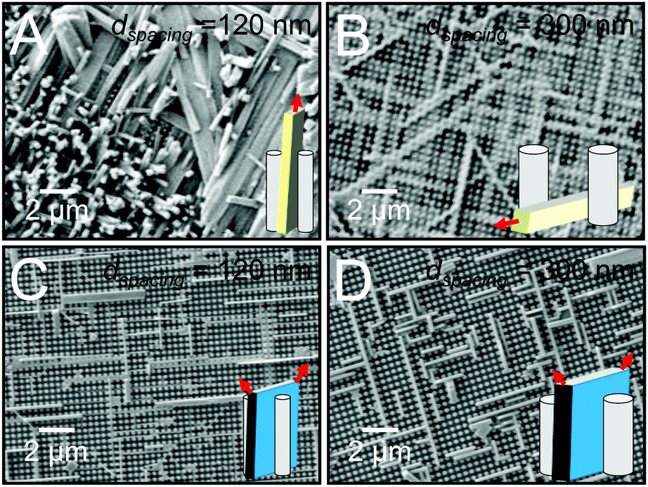 | ||
| Fig. 2 TIPS-PY crystals (n = 1) on nanopillar scaffolds (m = 2) with nanopillar diameters and edge-to-edge spacings of (A) 240 and 120 nm and (B) 600 and 300 nm, respectively. (C and D) Perylene crystals (n = 2) deposited on the same m = 2 scaffolds, respectively. Illustrations of crystal orientations relative to the nanopillars are provided as insets. Red arrows indicate the direction(s) of fast crystallization. | ||
In contrast, when the nanopillar edge-to-edge spacing was increased to dspacing = 300 nm, TIPS-PY crystals tended to align parallel to the substrate along the rows and columns in the x and y directions, and diagonal spaces between nanopillars, as displayed in Fig. 2B. At these larger spacings, the extent of confinement in the x and y directions is reduced. The tendency for crystals to orient with their fast growth directions aligned along the unconfined z direction is thus also reduced. These results indicate that when the dimensionality of the scaffold is greater than the crystal, i.e. m > n, scaffold-induced orientation control can only exist in one of the unconfined dimensions. In the case of nanopillar scaffolds, the unconfined dimensions are in the z direction parallel to the long axes of the nanopillars and in the x and y directions along the interstitial spaces between nanopillars.
In line with our previous work,24 perylene crystals deposited from solution into nanopillar scaffolds exhibited orientation in the x–y plane and in the z direction for both nanopillar edge-to-edge spacings, as displayed in Fig. 2C and D. In this system, m = n = 2. In the x–y plane parallel to the substrate surface, perylene crystals preferentially formed along the unconfined rows and columns in between nanopillars. In the z direction, perylene crystals oriented with their large-area faces perpendicular to the substrate surface. Considering that fast growth occurs along the direction of the corners for platelike crystals, neither of the two fast growth directions of the perylene crystals aligned with the unconfined directions of the nanopillar scaffold (refer to red arrows in inset). Instead, the fast growth directions were oriented at ∼45° angles from the z-axis. These directions correspond to the 〈010〉 and 〈001〉 crystallographic directions of α-perylene. For systems in which m = n = 2, these results indicate that orientation control can exist along the number of directions commensurate with the dimensionality of the crystals and scaffold. For n = 2 perylene crystals grown in m = 2 nanopillar scaffolds, crystal orientation can thus be controlled in two directions.
Scaffolds with m = 1
We next examined crystal growth in nanoporous scaffolds exhibiting cylindrical nanopores with m = 1. The depths of the nanopores were measured to be approximately 2 μm via cross-sectional SEM. Fig. 3A and B display top-view SEM images of TIPS-PY crystals grown from solution in nanopillar scaffolds with pore diameters of 125 and 250 nm. In these samples where m = n = 1, crystal orientation was controlled in the z direction along the unconfined long axis of the cylindrical nanopores. These results are in line with our previous findings on the use of nanoporous anodized aluminium oxide scaffolds to form vertical crystal arrays of TIPS-PY and other small-molecule organic semiconductors that form needle-like crystals.23 Furthermore, for pores in which crystallization occurred, one crystal per nanopore was generally observed. These nanoconfining scaffolds thus may also be used to control nucleation sites and crystal density.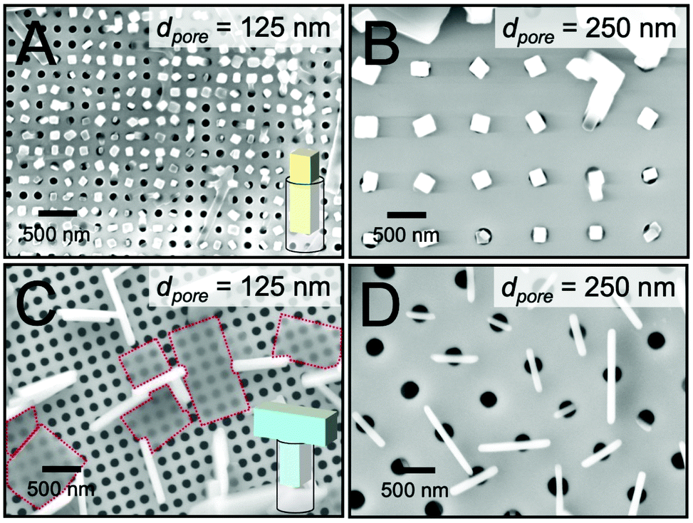 | ||
| Fig. 3 TIPS-PY crystals (n = 1) on nanoconfining scaffolds with cylindrical nanopores (m = 1) for nanopore diameters of (A) 125 nm and (B) 250 nm. (C and D) Perylene crystals (n = 2) deposited on the same m = 1 scaffolds, respectively. Illustrations of crystal shapes and orientations within the nanopores are provided in A and C. Red dashed lines highlight crystals that nucleated on top of the scaffold for clarity. | ||
Fig. 3C and D display top-view SEM images of perylene crystals grown inside cylindrical nanopores from solution. For scaffolds with nanopore diameters of 125 nm, two populations of perylene crystals were observed with the large faces of the crystals either parallel (highlighted with red dashed lines) or perpendicular to the substrate surface. We expect the former population of crystals nucleated above the scaffold while the latter nucleated within the scaffolds. For both populations of crystals, no preferred in-plane orientation was observed. The lack of preferred in-plane orientation suggests that orientation control is limited to the dimensionality of the scaffold. For these nanoporous scaffolds with m = 1, orientation can thus be controlled only along the z direction when nucleation occurs within the nanopores.
Intriguingly, the widths of the perpendicularly-oriented perylene crystals were found to be 6–8 times larger than the pore diameter. As displayed in the inset in Fig. 3C, we expect these crystals to form T-shapes. These unconventionally-shaped crystals are more obvious in scaffolds with larger pore diameters of 250 nm, as displayed in Fig. 3D. Again, no preferred in-plane orientation of the crystals was observed. The crystals were centered on the pores with one-to-one correspondence, indicating that they nucleated inside of the pores at a density of one nucleation event (or zero) per pore. Once the crystals reached the top surfaces of the pores where crystallization was no longer confined to the z direction, they resumed their native growth habit of fast crystallization along two directions to form T-shaped crystals.
T-Shaped perylene crystals
To more precisely determine the 3D shape of perylene crystals grown from cylindrical nanopores, the side profiles of these crystals were next examined. Fig. 4A displays an SEM image of perylene crystals grown from cylindrical nanopores (dpore = 250 nm) at a tilt angle of 54°. As observed from the figure, crystals that had not grown out of the pores appear as thin rectangular plates embedded within the pores (indicated by yellow arrows). At the top of the scaffold, m transitions from 1 to 3, allowing crystal growth to proceed unconfined in all directions. In general, the portions of the crystals grown above the scaffold adopted a rectangular shape. These crystals were asymmetric about the pore axis, with one “arm” of the T longer than the other. For the crystal oriented parallel to the plane of view of the image, for example, the arm lengths a and b were measured to be 210 and 340 nm. This difference in arm lengths suggests that nucleation occurred heterogeneously at the pore wall below the scaffold surface, as opposed to nucleating homogeneously in the center of the pore. The illustration in Fig. 4A displays the shape of a crystal that would be expected if nucleation occurs within the nanopore at the pore wall (nucleation center indicated by a red circle) and then continued growing above the scaffold. Heterogeneous nucleation may also occur at the bottom of the pores, which would result in the same T-shaped crystals.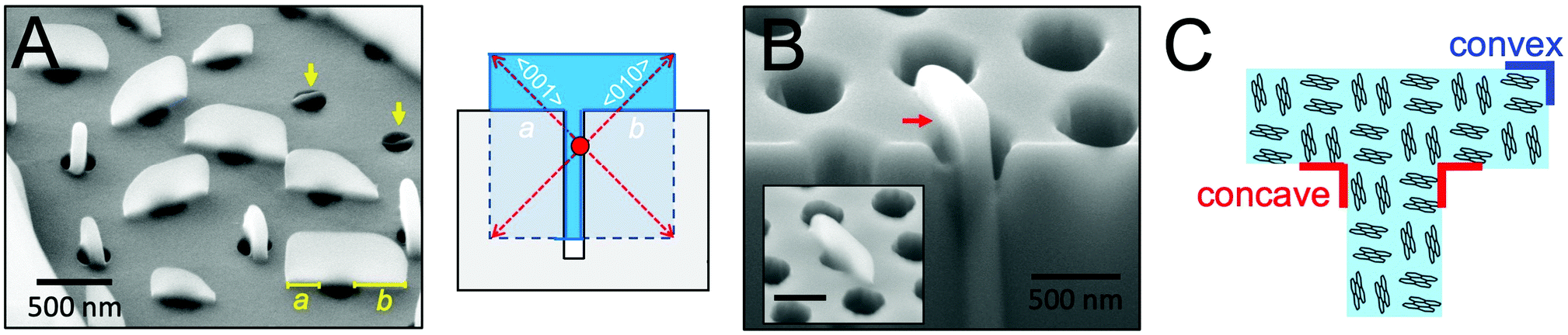 | ||
| Fig. 4 (A) SEM image of n = 2 perylene crystals grown in m = 1 cylindrical nanopores (dpore = 250 nm) collected at a tilt angle of 54°. Yellow arrows point to crystals that had nucleated within the nanopores but did not grow above the scaffold surface. Lengths of the T “arms” are also labeled as a and b for a crystal parallel to the plane of view of the image. Illustration depicts the morphology of a T-shaped crystal in which nucleation (red circle) occurred on the surface of the pore wall. (B) SEM image of a perylene crystal that nucleated inside a nanopore collected at a tilt angle of 54°. The substrate and part of the crystal were partially removed via focused ion beam etching to reveal the portion of the crystal embedded within the nanopore. Inset displays an SEM image of the same crystal before focused ion beam etching. A concave corner of the crystal formed at the scaffold surface is highlighted by a red arrow. (C) Illustration of the arrangement of perylene molecules with respect to the crystal shape displayed in B. | ||
Fig. 4B displays an SEM image of a T-shaped perylene crystal before (inset) and after focused ion beam etching was used to reveal the portion of the crystal within the nanopore. From this image, it is clear that crystal growth proceeded both within and above the pore to form a continuous single crystal. A sharp ∼90° concave corner can be observed at the point at which the crystal reached the top of the cylindrical nanopore. The arrangement of perylene molecules with respect to the crystal shape is provided in Fig. 4C. In this orientation where the fast crystallographic growth direction was aligned ∼45° rotated from the cylindrical pore long axis, the faces exposed at the convex and concave corners are the same due to crystal symmetry. For crystals oriented in other directions with respect to the long axis of the pores, on the other hand, higher surface energy planes may be revealed at the concave corners.
Concave surfaces are generally not observed in single crystals due to their higher surface free energy compared to convex or flat surfaces.26 Because such surfaces can be advantageous for various applications, such as catalysis, strategies, including site-specific dissolution or overgrowth and template-directed epitaxy, have been developed to grow nanocrystals with concave surfaces.27 Furthermore, preferential growth at sharp corners etched into single crystalline silicon has been observed, resulting in corner rounding.28 The ability to form sharp, concave corners in organic semiconductor crystals may thus provide an opportunity to study crystal growth mechanisms and photophysical properties at typically inaccessible crystallographic faces.
The formation of asymmetric organic semiconductor single crystals may also have applications in optical waveguiding. In 2015, for example, Wu and coworkers demonstrated formed organic single-crystal wires of semiconductor 9,10-bis(phenylethynyl)anthracene (BPEA) in nanogrooves.29 By controlling the nanogroove patterns, single-crystal wires could be connected at various angles. Optical waveguiding was observed along the wires, with some optical loss at the junction between wires. Because there are no grain boundaries within T-shaped perylene single crystals formed by partial nanoconfinement, these structures may provide a method for optical waveguiding and charge transport without associated losses at junctions.
Experimental methods
Nanoconfining scaffold fabrication
Si wafers (4 inches, single-side polished, p-type, 〈100〉 orientation, and 0–100 ohm resistance cm) were purchased from University Wafer Inc. and cleaned in piranha solution for 10 min, followed by deionized water for 5 min. Photoresist NR-7 1500 (Futurrex, Inc.) was spin-coated onto the wafers for 40 s at 3000 rpm, resulting in a film thickness of 1.5 μm. The wafers were then baked at 120 °C for 2 min. A He–Cd laser (50 mW and 30 cm coherence length at a wavelength of 325 nm) was used in Lloyd's mirror setup for holographic lithography to define the periodic nanopatterns.30,31 This method uses angle-dependent interference patterns between the direct and reflected laser light to define specific patterns of nanopillars or nanopores. The wafers were then post-baked at 100 °C for 1 min before being placed in an undiluted developer solution of RD6 (Futurrex, Inc.) for 12 s. The developed patterns were rinsed with deionized water for 3 min and blow-dried with nitrogen gas. Using the deep reactive ion etching (DRIE) technique, the silicon surfaces masked by the photoresist pattern were etched in cryogenic conditions (−100 °C). After the DRIE etching, the photoresist layer was removed by dissolving in piranha solution, followed by rinsing in deionized water and blow-drying by nitrogen gas. These samples were exposed to oxygen plasma for 10 min prior to organic semiconductor deposition.Organic semiconductor deposition
Triisopropylsilylethynyl pyranthrene (TIPS-PY) was synthesized according to previously published procedures.32 Prior to dip coating, nanopatterned TIPS-PY crystals were deposited onto nanopatterned silicon scaffolds via dip coating from 0.25 wt% solution in toluene at a temperature of 80 °C at a withdrawal speed of 0.4 mm min−1, according to previously published procedures.23 Perylene (purity ≥ 99%) was purchased from Sigma Aldrich and used without further purification. Perylene crystals were deposited onto nanopatterned silicon scaffolds via dip coating from a 0.0625 wt% solution in chloroform at a temperature of 70 °C and a withdrawal speed of 0.4 mm min−1, according to previously published procedures.24 For all experiments, the solutions were covered with aluminium foil to prevent rapid solvent evaporation during the dip coating process.Focused ion beam etching and SEM imaging
A FIB-SEM (Zeiss Auriga 40) was used to etch and image the samples. To etch the site-specific cross-sections, a 30 kV Ga+ FIB was used with the sample tilted to 54°. At this sample geometry, the cross-sectioned surface was directly exposed for imaging. A 2 kV SEM was used to image both top-view and cross-sectioned view surfaces of the samples.Conclusions
Control over organic semiconductor crystal orientation is critical for improving the performance of emerging organic electronic devices, yet remains elusive due to the rapid, uncontrolled nature of solution processing. The use of ordered scaffolds to impose order in these systems via dictating the location and orientation of nuclei during the initial stages of crystal growth has the potential to overcome processing limitations to align fast charge transport directions in crystals with the direction of current flow in devices. The design rules presented inform the selection of nanopatterned scaffold geometry based on the native growth habit of the organic semiconductor crystals by relating orientation control to the relative dimensionalities of the crystals and scaffolds. Excitingly, the ability to control crystal shape by spatially varying the scaffold dimensionality presents a unique opportunity to grow unconventional crystals with concave corners and asymmetric geometries, with implications in the areas of charge transport and optical waveguiding.Conflicts of interest
There are no conflicts to declare.Acknowledgements
S. S. L. acknowledges support from the National Science Foundation under Award Number CMMI-AM-1846178. The authors are also grateful for support from the PSEG Foundation to advance energy innovation at Stevens. C.-H. C. acknowledges support by the National Science Foundation under Award Number CMMI-MME-1462499. Research used microscopy resources within the Laboratory for Multiscale Imaging at Stevens Institute of Technology. Research was carried out in part at the Center for Functional Nanomaterials, Brookhaven National Laboratory, which is supported by the Department of Energy, Office of Basic Energy Sciences, under Contract No. DE-SC0012704.Notes and references
- S. Fratini, M. Nikolka, A. Salleo, G. Schweicher and H. Sirringhaus, Nat. Mater., 2020, 1–12 Search PubMed.
- V. C. Sundar, J. Zaumseil, V. Podzorov, E. Menard, R. L. Willett, T. Someya, M. E. Gershenson and J. A. Rogers, Science, 2004, 303, 1644–1646 CrossRef CAS.
- G. Giri, D. M. DeLongchamp, J. Reinspach, D. A. Fischer, L. J. Richter, J. Xu, S. Benight, A. Ayzner, M. He, L. Fang, G. Xue, M. F. Toney and Z. Bao, Chem. Mater., 2015, 27, 2350–2359 CrossRef CAS.
- Y. Diao, L. Shaw, Z. Bao and S. C. B. Mannsfeld, Energy Environ. Sci., 2014, 7, 2145–2159 RSC.
- L. Shaw, P. Hayoz, Y. Diao, J. A. Reinspach, J. W. F. To, M. F. Toney, R. T. Weitz and Z. Bao, ACS Appl. Mater. Interfaces, 2016, 8, 9285–9296 CrossRef CAS.
- K. Kotsuki, S. Obata and K. Saiki, Langmuir, 2014, 30, 14286–14291 CrossRef CAS.
- K. Kotsuki, S. Obata and K. Saiki, Langmuir, 2016, 32, 644–649 CrossRef CAS.
- K. Kim, E. J. G. Santos, T. H. Lee, Y. Nishi and Z. Bao, Small, 2015, 11, 2037–2043 CrossRef CAS.
- H. G. Zhang, J. T. Sun, T. Low, L. Z. Zhang, Y. Pan, Q. Liu, J. H. Mao, H. T. Zhou, H. M. Guo, S. X. Du, F. Guinea and H.-J. Gao, Phys. Rev. B: Condens. Matter Mater. Phys., 2011, 84, 245436 CrossRef.
- W. H. Lee, J. Park, S. H. Sim, S. Lim, K. S. Kim, B. H. Hong and K. Cho, J. Am. Chem. Soc., 2011, 133, 4447–4454 CrossRef CAS.
- J. M. Mativetsky, H. Wang, S. S. Lee, L. Whittaker-Brooks and Y.-L. Loo, Chem. Commun., 2014, 50, 5319–5321 RSC.
- D. L. Gonzalez Arellano, E. K. Burnett, S. Demirci Uzun, J. A. Zakashansky, V. K. Champagne, M. George, S. C. B. Mannsfeld and A. L. Briseno, J. Am. Chem. Soc., 2018, 140, 8185–8191 CrossRef CAS.
- K. Xiao, W. Deng, J. K. Keum, M. Yoon, I. V. Vlassiouk, K. W. Clark, A.-P. Li, I. I. Kravchenko, G. Gu, E. A. Payzant, B. G. Sumpter, S. C. Smith, J. F. Browning and D. B. Geohegan, J. Am. Chem. Soc., 2013, 135, 3680–3687 CrossRef CAS.
- Y. Wang, J. A. Torres, A. Z. Stieg, S. Jiang, M. T. Yeung, Y. Rubin, S. Chaudhuri, X. Duan and R. B. Kaner, ACS Nano, 2015, 9, 9486–9496 CrossRef CAS.
- X. Bai, K. Zong, J. Ly, J. S. Mehta, M. Hand, K. Molnar, S. Lee, B. Kahr, J. M. Mativetsky, A. Briseno and S. S. Lee, Chem. Mater., 2017, 29, 7571–7578 CrossRef CAS.
- B. D. Hamilton, I. Weissbuch, M. Lahav, M. A. Hillmyer and M. D. Ward, J. Am. Chem. Soc., 2009, 131, 2588–2596 CrossRef CAS.
- B. D. Hamilton, J.-M. Ha, M. A. Hillmyer and M. D. Ward, Acc. Chem. Res., 2012, 45, 414–423 CrossRef CAS.
- K. S. Park, B. Cho, J. Baek, J. K. Hwang, H. Lee and M. M. Sung, Adv. Funct. Mater., 2013, 23, 4776–4784 CAS.
- G. Giri, S. Park, M. Vosgueritchian, M. M. Shulaker and Z. Bao, Adv. Mater., 2014, 26, 487–493 CrossRef CAS.
- P. S. Jo, A. Vailionis, Y. M. Park and A. Salleo, Adv. Mater., 2012, 24, 3269–3274 CrossRef CAS.
- S. Watanabe, T. Fujita, J.-C. Ribierre, K. Takaishi, T. Muto, C. Adachi, M. Uchiyama, T. Aoyama and M. Matsumoto, ACS Appl. Mater. Interfaces, 2016, 8, 17574–17582 CrossRef CAS.
- X. Kong, K. Zong and S. S. Lee, Chem. Mater., 2019, 31, 4953–4970 CrossRef CAS.
- K. Zong, Y. Ma, K. Shayan, J. Ly, E. Renjilian, C. Hu, S. Strauf, A. Briseño and S. S. Lee, Cryst. Growth Des., 2019, 19, 3461–3468 CrossRef CAS.
- K. Zong, K. M. Asawa, A. Circelli, N. Sparta, C.-H. Choi and S. S. Lee, ACS Mater. Lett., 2020, 2, 721–726 CrossRef CAS.
- A. Pick, M. Klues, A. Rinn, K. Harms, S. Chatterjee and G. Witte, Cryst. Growth Des., 2015, 15, 5495–5504 CrossRef CAS.
- X. L. Li, G. Ouyang and G. W. Yang, Phys. Rev. B: Condens. Matter Mater. Phys., 2007, 75, 245428 CrossRef.
- H. Zhang, M. Jin and Y. Xia, Angew. Chem., Int. Ed., 2012, 51, 7656–7673 CrossRef CAS.
- K. Sudoh, H. Iwasaki, H. Kuribayashi, R. Hiruta and R. Shimizu, Surf. Sci., 2006, 600, L67–L70 CrossRef CAS.
- Y. Wu, J. Feng, X. Jiang, Z. Zhang, X. Wang, B. Su and L. Jiang, Nat. Commun., 2015, 6, 1–10 Search PubMed.
- I. Wathuthanthri, W. Mao and C.-H. Choi, Opt. Lett., 2011, 36, 1593 CrossRef.
- W. Mao, I. Wathuthanthri and C.-H. Choi, Opt. Lett., 2011, 36, 3176 CrossRef.
- L. Zhang, A. Fonari, Y. Zhang, G. Zhao, V. Coropceanu, W. Hu, S. Parkin, J.-L. Brédas and A. L. Briseno, Chem. – Eur. J., 2013, 19, 17907–17916 CrossRef CAS.
Footnote |
| † Current address: Molecular Design Institute, Department of Chemistry, New York University, New York, New York 10003, USA. E-mail: stephlee@nyu.edu |
| This journal is © The Royal Society of Chemistry 2021 |