
 Open Access Article
 This Open Access Article is licensed under a
 Creative Commons Attribution 3.0 Unported Licence
Low temperature CVD of thermoelectric SnTe thin films from the single source precursor, [nBu3Sn(TenBu)]†
Fred
Robinson
a,
Daniel W.
Newbrook
 b,
Peter
Curran
c,
C. H. (Kees)
de Groot
b,
Duncan
Hardie
c,
Andrew L.
Hector
a,
Ruomeng
Huang
b and
Gillian
Reid
*a
b,
Peter
Curran
c,
C. H. (Kees)
de Groot
b,
Duncan
Hardie
c,
Andrew L.
Hector
a,
Ruomeng
Huang
b and
Gillian
Reid
*a
aSchool of Chemistry, University of Southampton, Southampton SO17 1BJ, UK. E-mail: G.Reid@soton.ac.uk
bSchool of Electronics and Computer Science, University of Southampton, Southampton SO17 1BJ, UK
cDeregallera Ltd, Unit 2, De Clare Court, Pontygwindy Industrial Estate, Caerphilly CF83 3HU, UK
First published on 16th December 2020
Abstract
This work has demonstrated that the single source precursor [nBu3Sn(TenBu)], bearing n-butyl groups and containing the necessary 1![[thin space (1/6-em)]](https://www.rsc.org/images/entities/char_2009.gif) :1 Sn:Te ratio, facilitates growth of continuous, stoichiometric SnTe thin films. This single source CVD precursor allows film growth at significantly lower temperatures (355–434 °C at 0.01–0.05 Torr) than required for CVD from SnTe powder. This could be advantageous for controlling the surface states in topological insulators. The temperature-dependent thermoelectric performance of these films has been determined, revealing them to be p-type semiconductors with peak Seebeck coefficient and power factor values of 78 μV K−1 and 8.3 μW K−2 cm-1, respectively, at 615 K; comparing favourably with data from bulk SnTe. Further, we have demonstrated that the precursor facilitates area selective growth of SnTe onto the TiN regions of SiO2/TiN patterned substrates, which is expected to be beneficial for the fabrication of micro-thermoelectric generators.
:1 Sn:Te ratio, facilitates growth of continuous, stoichiometric SnTe thin films. This single source CVD precursor allows film growth at significantly lower temperatures (355–434 °C at 0.01–0.05 Torr) than required for CVD from SnTe powder. This could be advantageous for controlling the surface states in topological insulators. The temperature-dependent thermoelectric performance of these films has been determined, revealing them to be p-type semiconductors with peak Seebeck coefficient and power factor values of 78 μV K−1 and 8.3 μW K−2 cm-1, respectively, at 615 K; comparing favourably with data from bulk SnTe. Further, we have demonstrated that the precursor facilitates area selective growth of SnTe onto the TiN regions of SiO2/TiN patterned substrates, which is expected to be beneficial for the fabrication of micro-thermoelectric generators.
Introduction
With escalating concerns regarding climate change and a rapidly increasing demand for wireless power generation for sensors and other applications, thermoelectric materials are emerging as a key to advancement in both environmental and technological fields.1,2 Thermoelectric materials enable the conversion between heat and electricity and thus allow for both active cooling systems and the recycling of otherwise wasted heat energy.3,4 These processes rely on the Peltier and Seebeck effects, which are the conversion from electricity to cooling and the conversion of a heat gradient to the flow of charge, respectively.5 The materials that perform best for thermoelectric applications have a combination of high electrical conductivity, a large Seebeck coefficient and a low thermal conductivity. A useful, but not to be used alone, comparative value is the unitless figure of merit, ZT, which is described by the equation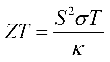 , where the Seebeck coefficient, S, the electrical conductivity, σ, the average temperature across the material, T and the thermal conductivity of the material, κ, are all brought together.6
One particular group of semiconducting materials, the metal chalcogenides, including the tellurides, shows great potential for thermoelectric applications. In particular, Bi2Te3 and Sb2Te3 are among the most promising thermoelectric materials for near room temperature applications, while PbTe has been used for mid-temperature applications, including for power generation in space, since the 1960s.5,7 However, due to the high toxicity of lead, alternative materials are desirable. A potential replacement for PbTe is SnTe, as it possesses many similarities to PbTe in both its crystal and electronic structures.8,9 SnTe exhibits an intrinsically high charge carrier concentration, which results in a relatively low Seebeck coefficient,10 but optimisation of the material through doping and alloying mean that SnTe offers great promise for thermoelectric applications.
SnTe has also gained significant interest due to the exciting properties relevant to other applications that it displays. Key examples are as a topological crystalline insulator,11,12 IR detection and radiation receivers13,14 and in near IR photovoltaics.15
Most previous work on the thermoelectric properties of SnTe relates to the bulk form, but given the low natural abundance of tellurium, the sustainability of bulk tellurium-based thermoelectrics is questionable. On the other hand, the quantity of material required for thin film based thermoelectric microgenerators is very considerably reduced (by >95%), leading to the prospect of using this in internet of things (IoT) based applications. While physical vapour deposition (PVD)14 and molecular beam epitaxy via co-evaporation of elemental tin and tellurium16 have been used to grow thin films of SnTe, chemical vapour deposition (CVD) is an attractive processing technique for the production of thin film coatings and is widely used in industry due to its scalability over large and complex surfaces, high deposition rates, low cost and adaptability to different material targets and precursor types.17
SnTe nanowires, nanocrystals and other low dimensional nanostructures have been obtained via vapour–solid (VS) or vapour–liquid–solid (VLS) growth from SnTe powder at elevated temperatures (typically 500–600 °C).18–20 Jarabek and co-workers produced SnTe powder by pyrolysing the trimeric precursor (Bn2SnTe)3 (Bn = CH2C6H5) at 400 °C,21 while Wang and co-workers reported that spin-coating and annealing the product from reaction of Sn with Ph2Te2 in 1,2-diaminoethane deposited SnTe films,22 and Johnson and co-workers have used the compounds [(PhTe)2Sn{N(SiMe3)2}2] and [{(Me3Si)2N}2Sn(μ2-Te)]2 as precursors for SnTe nanoparticles.23 There have also been a small number of reports describing the CVD growth of SnTe thin films. Ahmet et al. have reported the tin guanidinate complex, [{CyNC(NMe2)NCy}Sn(Te)], as a single source precursor for the aerosol-assisted CVD of SnTe onto Si from a toluene solution, albeit giving very thin films and with some SnO contamination,24 while Chuprakov et al. have used [Sn{(SiMe3)2CH}2(μ-Te)]2 in a metal–organic CVD set-up to produce SnTe films.25 In the latter, the high carrier gas (1:1 He/H2) flow rate helps to transport the single source precursor to the substrate and encourage the deposition, and this system shows higher deposition rates onto metallic surfaces over insulating surfaces. Our own work has shown that single source precursors based on complexes of p-block halides with neutral chalcogenoether ligands, such as [SnCl4{BuE(CH2)3EBu}] (E = S, Se) and [BiCl3(E′Bu2)3] (E′ = Se, Te) are effective for the growth of SnE2 or SnE26 thin films (depending upon the deposition conditions) and Bi2E′327 thin films, respectively. Moreover, these precursors also allow discrimination between the different surfaces of lithographically patterned substrates, leading to preferential growth onto the TiN surface on a patterned TiN/SiO2 substrate. In contrast to the success achieved using the precursors based on thio- and seleno-ether complexes of SnCl4, low pressure CVD using the corresponding telluroether complex, [SnCl4{BuTe(CH2)3TeBu}], is not suitable for the CVD growth of the corresponding SnTe films, instead leading to the deposition of elemental tellurium only.26
In pursuit of an effective single source precursor suitable for SnTe thin film deposition, we report here the high yield preparation of the molecular reagent, [nBu3Sn(TenBu)], and demonstrate its application for the deposition of continuous thin films of cubic SnTe via low pressure CVD. [nBu3Sn(TenBu)] has been mentioned in the patent literature as a CVD precursor for SnTe, however, with minimal information regarding the precursor synthesis and characterisation, or the nature and characteristics of the resulting deposit.28 The composition, morphology and structure of the resulting thin films have been determined by XRD, SEM, EDX analysis and Raman spectroscopy. We also present their thermoelectric properties, including variable temperature Seebeck coefficient, electrical conductivity and power factor measurements, along with variable temperature Hall effect coefficients, charge carrier concentrations, mobility measurements as well as the selective deposition of SnTe onto patterned substrates.
Experimental
All reactions were performed under an inert atmosphere using Schlenk, vacuum line and dry nitrogen glove box techniques. The solvents used (THF, toluene and hexane) were dried by distillation from sodium wire prior to use and NMR solvents were stored in a glovebox over molecular sieves. nBu3SnCl (Aldrich) was stored in a glovebox and used as received. All 1H, 13C{1H}, 119Sn{1H} (referenced against neat SnMe4), 125Te{1H} (referenced against neat TeMe2) and 2D HSQC NMR spectra were collected on a Bruker AV400 spectrometer in CDCl3. Microanalyses were obtained via the London Metropolitan University elemental analysis service.The volatility was determined using a temperature ramp experiment via TGA. This experiment was conducted by measuring approximately 5 mg of [nBu3Sn(TenBu)] into an alumina crucible inside a dry, nitrogen-filled glove box. The crucible was then quickly transferred to the TGA where it was immediately put under a flow of argon gas. The precursor was then heated at a ramp rate of 5 °C min−1 under a constant flow of argon gas from 30–600 °C.
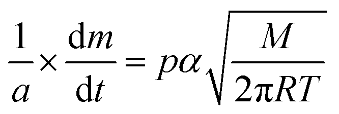
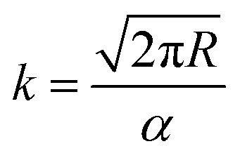
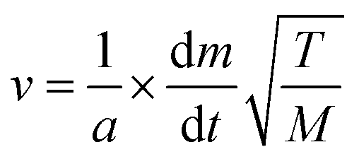
The vapour pressure approximations were obtained using an isothermal step experiment using TGA to obtain the rate of mass lost at 50, 75, 100 and 125 °C under the flow of argon gas at a flow rate of 60 mL min−1. All temperatures were stabilised for 1 hour and the ramp rate to each temperature was 5 °C min−1. This was initially performed for the reference compound used, tetrakis-t-butyltin as values for its vapour pressure are available within the literature.29 The measured values were then used to calculate the instrument constants related to the equipment, at which point the vapour pressures of the single source precursors could be obtained using the calculations below, as demonstrated by Wang et al.30
 | (1) |
 | (2) |
 | (3) |
| p = kv | (4) |
 is the rate of mass loss, T is the temperature and M is the relative molecular mass. Using these the final equation gives the vapour pressure, p. At each of the temperatures measured the value of k was first calculated using the experimentally determined value for v and the known value for p.29 Using the value for k gained in this method, the vapour pressure of the single source precursor could be calculated.
Synthesis of [nBu3Sn(TenBu)]
Tellurium granules (2.846 g, 2.23 × 10⁻² mol) were ground into a fine powder under an inert atmosphere in the glovebox before being suspended in THF (30 mL). The suspension was then frozen in liquid nitrogen (77 K) before the dropwise addition of nBuLi solution in hexanes (13 mL, 2.18 × 10⁻² mol). After the mixture had slowly thawed, the solution initially turned yellow and then red. Further nBuLi solution (0.3 mL, 5.03 × 10⁻⁴ mol) was then added dropwise until a pale yellow colour persisted. A solution of nBu3SnCl (6.856 g, 2.11 × 10⁻³ mol) in THF (30 mL) was then added dropwise, while it was cooled using an ice bath. The reaction mixture was stirred vigorously for 24 h, leaving an orange solution. The volatiles were then removed in vacuo and the orange oily residue was then washed twice with hexane (30 mL), leading to the precipitation of LiCl. This was removed by cannula filtration before the filtrate was taken to dryness in vacuo, leaving an orange oil. The compound is somewhat moisture sensitive and was therefore handled and stored under an inert atmosphere to avoid degradation, although it can be handled briefly in air without degradation. Yield 8.608 g, 86%. Elemental analysis: calc. for C16H36SnTe (474.77): C 40.48, H 7.64%. Found: C 40.60, H 8.65%. 1H NMR (CDCl3): δ/ppm = 0.90 (two overlapping t, J = 8.00 Hz, [12H]), 1.19 (t with 119Sn satellites, [6H]), 1.34 (overlapping m, [8H]), 1.55 and 1.65 (overlapping m, [8H]), 2.52 (t with overlapping 125Te satellites, [2H]). 13C{1H} NMR (CDCl3): δ/ppm = −7.05 (1J125Te13C = 133 Hz, 2J119Sn13C = 13 Hz, CH2), 12.54 (1J119Sn13C = 299 Hz, 1J117Sn13C = 286 Hz, CH2), 13.27 (CH3), 13.61 (CH3), 25.01 (CH2), 26.96 (2J119Sn13C = 63 Hz, CH2), 29.69 (3J119Sn13C = 21 Hz, CH2), 37.34 (3J125Te13C = 8 Hz CH2). 119Sn{1H} NMR (CD2Cl2/CH2Cl2): δ/ppm = −15.62 (1J119Sn125Te = 2765 Hz). 125Te{1H} NMR (CD2Cl2/CH2Cl2): δ/ppm = −536.51 (1J119Sn125Te = 2704 Hz).Thin film growth by low pressure CVD onto fused silica substrates
The fused silica substrates (8 mm × 20 mm) were washed with deionised water, followed by ethanol, before being dried thoroughly in an oven before use. In a LPCVD experiment the precursor is loaded (5–40 mg) into a closed end silica tube (1 cm diameter, 45 cm long). With the tube held horizontally, this was followed by the substrates placed next to one another (lengthways along the tube starting closest to the precursor bulb). The assembly of the CVD tube is performed under an inert atmosphere inside a glovebox before being moved into position in a tube furnace, insulated using silica wool at both ends, and being placed under a constant reduced pressure (0.01–0.05 mmHg). The Lenton (LTF 12/50/300) tube furnace was then brought to temperature (furnace set temperature = 475 °C; substrate temperature where deposition observed = 355 to 434 °C). Once the desired temperature had been reached the tube was repositioned to bring the precursor bulb closer to the hot zone so that volatilisation could commence (the temperature at the precursor bulb was between 274 to 355 °C, with a rate of mass transfer of between 1.72 and 3.09 mg min−1). The time taken for the deposition to occur once the tube furnace was at temperature was typically 5–18 min (the rates of growth were between 64 and 125 nm min−1). After cooling and letting down to a dinitrogen atmosphere, the CVD tube was transferred back into the glovebox where the substrates onto which the films had deposited were removed and stored. The low pressure CVD experiments produced light grey films of SnTe with typical coverage of 1–4 cm × 0.8 cm.Thin film growth by low pressure CVD onto patterned SiO2/TiN substrates
TiN/SiO2 patterned substrates (8 mm × 20 mm) were prepared as described previously.26 These were loaded lengthways into a closed end silica tube containing <3 mg of the [nBu3Sn(TenBu)] precursor. The deposition process parallels that onto the unpatterned substrates, with the subtle differences of the lower precursor loading and the position of the tube causing the slower volatilisation of the precursor (and hence better discrimination of the TiN vs. SiO2 surfaces), thus the duration of the depositions is longer (30–45 min).Thin film characterisation
Grazing incidence X-ray diffraction (XRD) patterns were collected using a Rigaku SmartLab system (Cu-Kα, λ = 1.5418 Å) with parallel X-ray beam and a Hypix detector in 1D mode. A 2θ scan range of 10–80° and an incident angle (ω-offset) of 1° were used. The crystalline phase of the film was determined by comparison with a literature XRD pattern, accessed via the Inorganic Crystal Structure Database (ICSD),31 and lattice parameters were obtained by further optimisation of the fit using PDXL.32The scanning electron microscope used was a FEI XL30 ESEM with a tungsten filament electron source and ThermoFisher UltraDry EDX, 10 mm2 detector. The SEM images were all captured at magnifications of 2000, 5000 and 10000 times at accelerating voltages of either 10 or 15 keV. The Raman spectra were obtained using a Renishaw inVia confocal Raman microscope with a 785 nm laser. The incident laser power was adjusted to 2.5 mW for all samples.
Thermoelectric and electrical property measurements
Variable temperature resistivity, carrier concentration, and carrier mobility were determined by Hall measurements (Nanometrics HL5500PC) from 125 to 450 K in steps of 25 K under a magnetic field of 0.5 T. Care was taken to ensure linear contact between the probes and sample before each measurement and the current was optimised to ensure normal Ohmic conduction with maximum voltage signal. Variable temperature Seebeck coefficient and electrical resistivity were measured using the Joule Yacht MRS-3L from 300 to 600 K in steps of 25 K. The Seebeck coefficient was measured using the differential method with a maximum temperature difference of 10 K. The resistivity was measured using a 4-point probe method and corrected for geometric error using the results from the Hall measurement system.Results and discussion
Synthesis and characterisation of the [nBu3Sn(TenBu)] precursor
The organometallic tin(IV) compound, [nBu3Sn(TenBu)], was selected as a potentially viable single source precursor for the deposition of SnTe thin films since the n-butyl substituents on both the tin and tellurium provide a clean and low energy decomposition pathway via β-hydride elimination, the 1:1 Sn:Te ratio in the precursor should aid deposition of the targeted binary phase and avoid incorporation of excess Te, while the volatility of the precursor (oil) was anticipated to be well-suited to a low pressure CVD procedure.33 Previous work has shown that film thin deposition from CVD precursors containing n-butyl and other alkyl substituents containing β-hydrogen atoms can often involve β-hydride elimination34 of alkene and reductive elimination of hydrogen gas or alkane. Moreover, we have shown that nBu groups can also enhance the prospects of highly area selective deposition of metal chalcogenides onto patterned substrates.26,27
The precursor synthesis (Scheme 1) required the initial formation of LiTenBu at low temperature (to prevent the formation of nBu2Te235), followed by a salt metathesis step to form the final product and lithium chloride, which were separated by filtration. This procedure produced an orange oil in excellent (86%) yield, which was shown to be pure [nBu3Sn(TenBu)], without the need for any further purification, by means of microanalysis, 1H, 13C{1H}, 119Sn{1H} and 125Te{1H} NMR spectroscopy (Experimental).
 | ||
| Scheme 1 Synthesis route to [nBu3Sn(TenBu)]. | ||
Thermogravimetric analysis (TGA) (Fig. 1a) shows that complete (100%) mass loss occurs by T ∼265 °C. The onset of evaporation occurs at ∼110 °C, and while the TGA profile may hint towards mass loss possibly occurring in multiple stages, no steps are evident in the DTA profile. The data therefore indicate that at 1 atm pressure under an inert gas, complete evaporation of the precursor occurs.
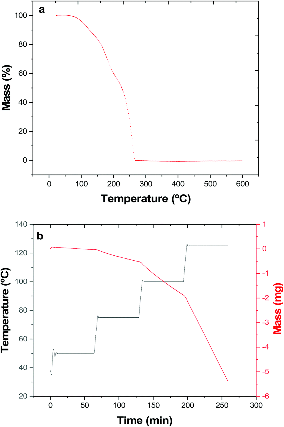 | ||
| Fig. 1 (a) Thermogravimetric analysis of [nBu3Sn(TenBu)] showing the percentage mass loss with temperature at a ramp rate of 5 °C min−1 and a constant flow of argon gas. (b) Isothermal step TGA experiment of [nBu3Sn(TenBu)] used for vapour pressure determination. | ||
The vapour pressure as a function of temperature was also determined isothermally (Fig. 1b and Table 1).
| Temperature (K) | n Bu4Sn vapour pressure (Pa)36 | [nBu3Sn(TenBu)] vapour pressure (Pa) |
|---|---|---|
| 323.15 | 17 | 3 ± 1 |
| 348.15 | 70 | 23 ± 4 |
| 373.15 | 240 | 80 ± 13 |
| 398.15 | 703 | 233 ± 37 |
| T vap | 518.15 K | 473.15 Ka |
| ΔHvap | 53 kJ mol−1 (67.8 kJ mol−1) | 67 kJ mol−1 ± 15 |
| ΔSvap | 100 J K−1 mol−1 (130 J K−1 mol−1) | 140 J K−1 mol−1 ± 32 |
SnTe thin film growth
Low pressure CVD experiments were undertaken using a typical loading of around ∼30 mg of precursor. The deposition occurred on the substrate tiles placed nearest the precursor bulb where the vaporised precursor had the shortest distance to travel. The deposits formed were white or light grey in appearance. Grazing incidence XRD analysis, as shown in Fig. 2, confirmed that the films produced were formed of cubic SnTe (space group Fm![[3 with combining macron]](https://www.rsc.org/images/entities/char_0033_0304.gif) m), in good agreement with the literature data for bulk SnTe.8 The refined lattice parameter a = 6.3033(4) Å, with Rwp of 12.59 (literature: a = 6.318(3) Å).8
m), in good agreement with the literature data for bulk SnTe.8 The refined lattice parameter a = 6.3033(4) Å, with Rwp of 12.59 (literature: a = 6.318(3) Å).8
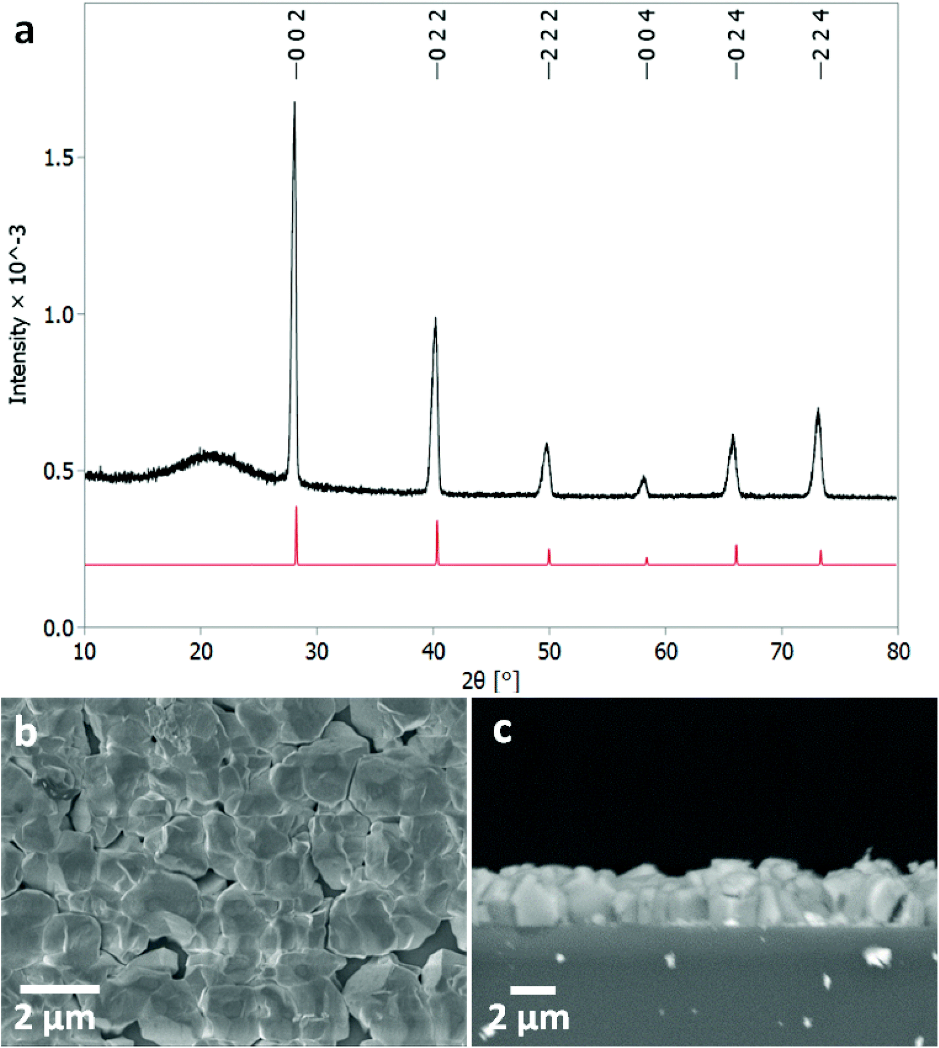 | ||
| Fig. 2 (a) Grazing incidence XRD pattern for SnTe thin film (thickness ∼2 μm) with XRD pattern for bulk cubic SnTe (Fmm) (red).8 The broad feature observed around 21° is due to the fused silica substrate beneath the SnTe film. Top down SEM (b) and cross-sectional SEM (c) of a SnTe film. | ||
Crystallite sizes of between 100(10) to 210(110) nm were measured using the Halder–Wagner method, using a LaB6 standard to account for instrumental peak broadening effects. The sizes measured using this method are smaller than those seen in the SEM images, which indicates that those observed in the SEM images are most likely particles of crystalline aggregates rather than individual crystallites.
The scanning electron microscopy (SEM) analysis (Fig. 2) showed uniformly distributed arrays of continuous polycrystalline films comprised of block-like particles. The cross-sectional SEM analysis determined the film thickness to be around ∼1–2 μm and the grain size is around 1 μm.3
Energy dispersive X-ray analysis showed that all the films had compositions within experimental error of stoichiometric SnTe (Table 2). Peaks corresponding to Si and O from the underlying substrates were present in a few samples (indicating thinner films), but no impurities were evident. This was also supported by Raman scattering, which showed only features expected for SnTe, with the A1 and E modes at 124 and 143 cm−1, respectively (Fig. 3), and with no contamination evident.11,37
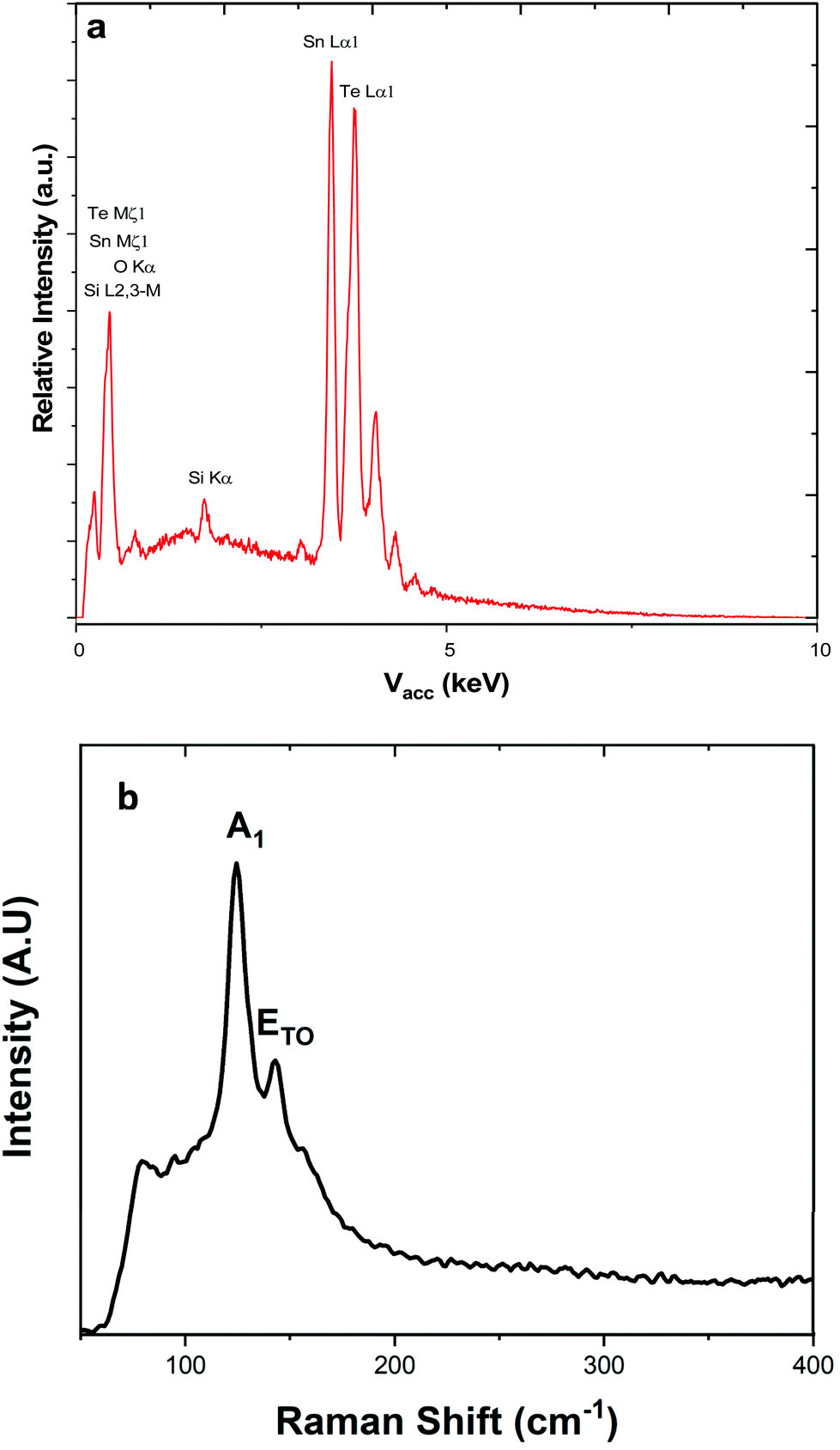 | ||
| Fig. 3 (a) EDX spectrum highlighting the elements present within the SnTe film, the silicon present is attributed to the substrate. (b) Raman spectrum with the data highlighting the A1 and E modes at 124 and 143 cm−1, respectively.1 | ||
Thermoelectric measurements
In order to evaluate the thermoelectric performance of the SnTe thin films deposited via our CVD process, the temperature-dependent Hall and Seebeck measurements were conducted. The as-deposited SnTe film exhibits a metallic transportation behaviour with room temperature electrical conductivity of 2434 S cm−1 (Fig. 4a). This high electrical conductivity can be ascribed to the intrinsic Sn vacancy induced p-type carrier concentration.10 This is confirmed by the Hall measurement results where high p-type carrier concentrations in the range between (4–5) × 1021 cm−3 were observed, as shown in Fig. 4b. While this carrier concentration remains relatively constant, the mobility decreases from ca. 5 cm2 V−1 s−1 to 3 cm2 V−1 s−1 as the temperature increases from 100 K to 450 K. This is likely to be caused by the stronger lattice scattering at elevated temperatures, resulting in the reduction of electrical conductivity.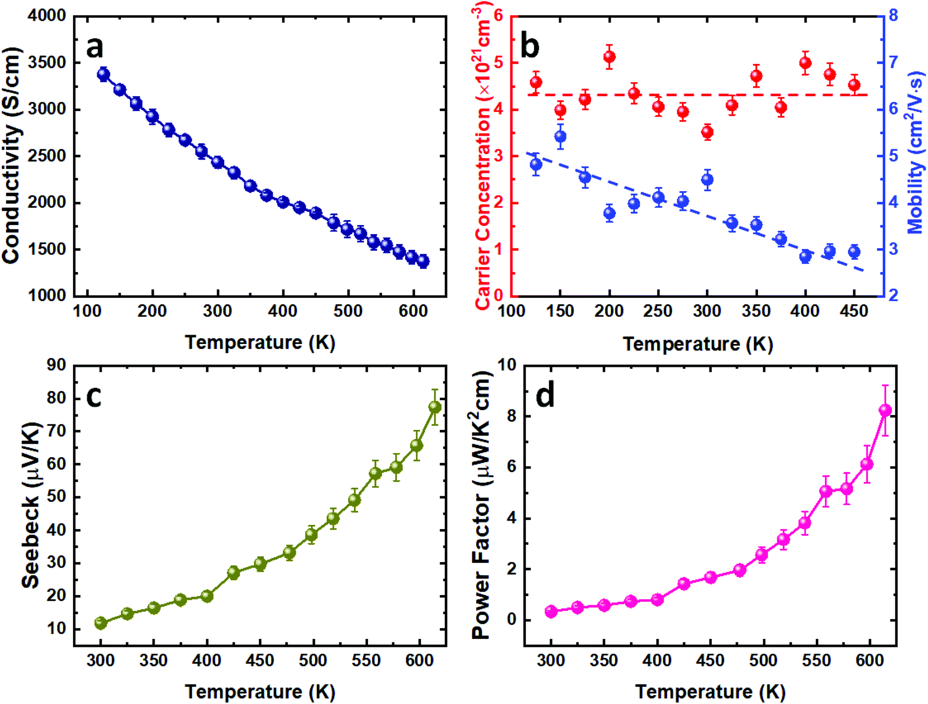 | ||
| Fig. 4 Temperature dependence of (a) the electrical conductivity, (b) carrier concentration and mobility, (c) Seebeck coefficient and (d) power factor for the as-deposited SnTe thin film. All lines to guide the eyes. | ||
Fig. 4c presents the temperature dependent Seebeck coefficient of the as-deposited SnTe thin film. The p-type conductivity is further confirmed by the positive Seebeck coefficient values obtained. The Seebeck coefficient for the as-deposited SnTe film is ca. 12 μV K−1 at room temperature and is increased to ca. 78 μV K−1 at higher temperature (615 K). The power factor of the SnTe film is shown in Fig. 4d, with a peak value of 8.3 μW K−2 cm−1 at 615 K. These results are comparable to the other reported values for undoped SnTe samples,10,38–40 also confirming the high quality of the SnTe films produced from the single source precursor used in this work. It is worth mentioning that high hole carrier concentration and large energy separation (ca. 0.3–0.4 eV) between light hole and heavy hole valence bands have limited the thermoelectric properties of un-doped SnTe.41 Significant improvements in the Seebeck coefficient of bulk SnTe have been achieved by pioneering works using doping/alloying to induce valence band convergence.40–42 We have also demonstrated recently the capability of alloying Bi2Te3 thin films with both Bi2Se3 and Sb2Te3 using single source precursors.43 Future work will explore using a similar strategy to further improve the thin film SnTe thermoelectric performance.
Selective deposition of SnTe onto patterned substrates
We have previously demonstrated selective deposition for a range of metal chalcogenide materials onto specific regions of lithographically patterned substrates using tailored single source precursors.26,27 A correlation between the electrical conductivity of the film and the selective deposition performance has been established, with higher conductivity leading to enhanced selectivity.41 We have also shown that deposition of the highly conductive SnTe onto TiN/SiO2 patterned substrates in this work results in selective growth on the TiN surface in preference to the SiO2 surface, as shown Fig. 5a. EDX spectra (Fig. 5b) on the TiN surface (yellow rectangular area in Fig. 5a) clearly shows the existence of Sn and Te, while only Si and O peaks can be observed from the EDX data taken on the SiO2 surface (red rectangular area in Fig. 5a). This selective deposition behaviour is further demonstrated by EDX element mapping (Fig. 5c–f) where the Sn and Te are almost entirely confined to the TiN areas of the pattern. It is worth mentioning that the selective deposition behaviour allows great positional control over the material growth and is beneficial for the fabrication of micro-thermoelectric generators.44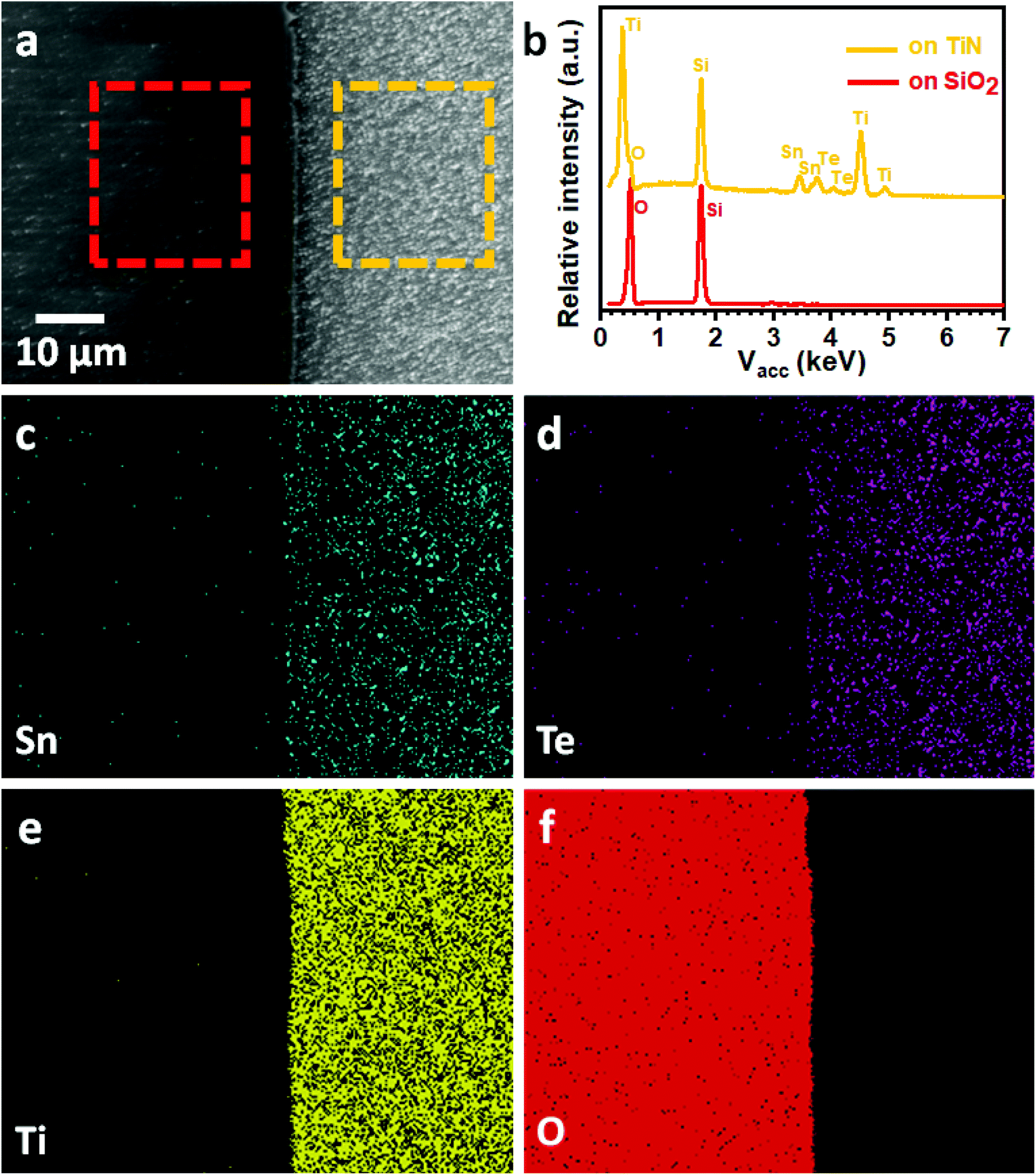 | ||
| Fig. 5 (a) Top-view SEM image of a TiN/SiO2 patterned substrate with SnTe selectively deposited on the TiN surface (right). (b) EDX spectra taken from the rectangular areas indicated in (a). EDX element mapping of (c) Sn, (d) Te, (e) Ti and (f) O. | ||
Conclusions and outlook
This work has demonstrated that the single source precursor [nBu3Sn(TenBu)], bearing n-butyl groups and containing the required 1:1 Sn:Te ratio, facilitates low pressure CVD growth of continuous, stoichiometric SnTe thin films very effectively. The temperature-dependent thermoelectric performance of these films confirms them to be p-type semiconductors with peak Seebeck coefficient and power factor values of 78 μV K−1 and 8.3 μW K−2 cm−1, respectively, at 615 K, comparing favourably with data from bulk SnTe. We have also demonstrated that this precursor facilitates selective growth of SnTe onto the TiN regions of SiO2/TiN patterned substrates, which is expected to be beneficial for the fabrication of micro-thermoelectric generators.
This single source precursor also allows for SnTe film growth at a significantly lower temperature than that required for CVD from SnTe powder, which is expected to be advantageous for controlling the surface states in topological insulators.
Conflicts of interest
The authors have no conflicts to declare.Acknowledgements
We thank the EPSRC for a CASE studentship to F. R. (EP/N509747/1) and an iCASE studentship to D. W. N. We also thank Deregallera Ltd and BAE Systems for funding for F. R. and D. W. N., respectively.References
- X. F. Zheng, C. X. Liu, Y. Y. Yan and Q. Wang, Renewable Sustainable Energy Rev., 2014, 32, 486 CrossRef CAS.
- M. Haras and T. Skotnicki, Nano Energy, 2018, 54, 461 CrossRef CAS.
- P. Douglas, in ICT – Energy – Concepts Towards Zero – Power Information and Communication Technology, 2014, p. 49 Search PubMed.
- J. Yan, X. Liao, D. Yan and Y. Chen, J. Microelectromech. Syst., 2018, 27, 1 CAS.
- C. Wood, Rep. Prog. Phys., 1988, 51, 459 CrossRef CAS.
- R. A. Smith, Physics of Semiconductors, New York, 1960 Search PubMed.
- A. Polozine, S. Sirotinskaya and L. Schaeffer, Mater. Res., 2014, 17, 1260 CrossRef.
- P. Bauer Pereira, I. Sergueev, S. Gorsse, J. Dadda, E. Müller and R. P. Hermann, Phys. Status Solidi B, 2013, 250, 1300 CrossRef CAS.
- W. Li, L. Zheng, B. Ge, S. Lin, X. Zhang, Z. Chen, Y. Chang and Y. Pei, Adv. Mater., 2017, 29, 1605887 CrossRef.
- A. Banik, S. Roychowdhury and K. Biswas, Chem. Commun., 2018, 54, 6573 RSC.
- N. Berchenko, R. Vitchev, M. Trzyna, R. Wojnarowska-Nowak, A. Szczerbakow, A. Badyla, J. Cebulski and T. Story, Appl. Surf. Sci., 2018, 452, 134 CrossRef CAS.
- J. Shen and J. J. Cha, Nanoscale, 2014, 6, 14133 RSC.
- D. J. Lewis, P. Kevin, O. Bakr, C. A. Muryn, M. A. Malik and P. O'Brien, Inorg. Chem. Front., 2014, 1, 577 RSC.
- H. Zhang, B. Man and Q. Zhang, ACS Appl. Mater. Interfaces, 2017, 9, 14067 CrossRef CAS.
- R. Moshwan, L. Yang, J. Zou and Z. G. Chen, Adv. Funct. Mater., 2017, 27, 30 CrossRef.
- A. A. Taskin, F. Yang, S. Sasaki, K. Segawa and Y. Ando, Phys. Rev. B: Condens. Matter Mater. Phys., 2014, 89, 121302 CrossRef.
- H. O. Pierson, Handbook of Chemical Vapour Depostion: Principles, Technology and Applications, Noyes Publications/William Andrew Publishing LLC, Norwich, 2nd edn, 1992 Search PubMed.
- P. Liu, Y. Xie, E. Miller, Y. Ebine, P. Kumaravadivel, S. Sohn and J. J. Cha, J. Phys. Chem. Solids, 2019, 128, 351 CrossRef.
- M. Safdar, Q. Wang, M. Mirza, Z. Wang, K. Xu and J. He, Nano Lett., 2013, 13, 5344 CrossRef CAS.
- Y. Zou, Z. Chen, J. Lin, X. Zhou, W. Lu, J. Drennan and J. Zou, Nano Res., 2015, 8, 3011 CrossRef CAS.
- P. Boudjouk, M. P. Remington, D. G. Grier, W. Triebold and B. R. Jarabek, Organometallics, 1999, 18, 4534 CrossRef CAS.
- Z. Wong, Y. Ma, P. B. Vartak and R. Y. Wang, Chem. Commun., 2018, 54, 9055 RSC.
- J. B. Thompson, I. Y. Ahmet, A. L. Johnson and G. Kociak-Kohn, Eur. J. Inorg. Chem., 2016, 4711 CrossRef CAS.
- I. Y. Ahmet, M. S. Hill, P. R. Raithby and A. L. Johnson, Dalton Trans., 2018, 47, 5031 RSC.
- I. S. Chuprakov, K. H. Dahmen, J. J. Schneider and J. Hagen, Chem. Mater., 1998, 10, 3467 CrossRef CAS.
- C. H. de Groot, C. Gurnani, A. L. Hector, R. Huang, M. Jura, W. Levason and G. Reid, Chem. Mater., 2012, 24, 4442 CrossRef CAS.
- S. L. Benjamin, C. H. de Groot, C. Gurnani, A. L. Hector, R. Huang, E. Koukharenko, W. Levason and G. Reid, J. Mater. Chem. A, 2014, 2, 4865 RSC.
- Method for preparing crystalline compounds AIVABVIA, 5904/77, 1977, 1518264.
- D. Hawker, Chemosphere, 1992, 25, 427 CrossRef CAS.
- C. Wang, S. Yang and Y. Chen, R. Soc. Open Sci., 2019, 6, 181193 CrossRef CAS.
- ICSD: Inorganic Crystal Structure Database (ICSD), Fachinformationszentrum Karlsruhe (FIZ), accessed via the EPSRC funded National Chemical Database Service hosted by the Royal Society of Chemistry.
- S. Graulis, D. Chateigner, R. T. Downs, A. F. T. Yokochi, M. Quirós, L. Lutterotti, E. Manakova, J. Butkus, P. Moeck and A. Le Bail, J. Appl. Crystallogr., 2009, 42, 726 CrossRef.
- S. L. Hawken, R. Huang, C. H. de Groot, A. L. Hector, M. Jura, W. Levason, G. Reid and G. B. G. Stenning, Dalton Trans., 2019, 48, 117 RSC.
- P. J. Davidson, M. F. Lappert and R. Pearce, Chem. Rev., 1976, 76, 219 CrossRef CAS; C. J. Jenks, M. Xi, M. X. Yang and B. E. Bent, J. Phys. Chem., 1994, 98, 2152 CrossRef; J. G. Forbes and A. J. Gellman, J. Am. Chem. Soc., 1993, 115, 6277–6283 CrossRef; S. Wang, M. L. McCrea-Hendrick, C. M. Weinstein, C. A. Caputo, E. Hoppe, J. C. Fettinger, M. M. Olmstead and P. P. Power, J. Am. Chem. Soc., 2017, 139, 6596 CrossRef.
- E. G. Hope, T. Kemmltt and W. Levason, Organometallics, 1987, 6, 206 CrossRef CAS.
- G. G. Devyatykh, V. A. Umilin and Y. N. Tsinovoi, Bull. Acad. Sci. USSR, 1970, 19, 497 CrossRef; J. V. Davies, A. E. Pope and H. A. Skinner, Trans. Faraday Soc., 1963, 53, 2233 RSC.
- C. An, K. Tang, B. Hai, G. Shen, C. Wang and Y. Qian, Inorg. Chem. Commun., 2003, 6, 181 CrossRef CAS.
- Q. Jiang, H. Hu, J. Yang, J. Xin, S. Li, G. Viola and H. Yan, ACS Appl. Mater. Interfaces, 2020, 12, 23102 CrossRef CAS.
- Z. Ma, C. Wang, J. Lei, D. Zhang, Y. Chen, J. Wang, Z. Cheng and Y. Wang, ACS Appl. Energy Mater., 2019, 2, 7354 CrossRef CAS.
- A. Doi, S. Shimano, D. Inoue, T. Kikitsu, T. Hirai, D. Hashizume, Y. Tokura and Y. Taguchi, APL Mater., 2019, 7, 091107 CrossRef.
- R. Moshwan, W.-D. Liu, X. L. Shi, Y. P. Wang, J. Zou and Z. G. Chen, Nano Energy, 2019, 65, 104056 CrossRef CAS.
- L. Zhao, J. Wang, J. Li, J. Liu, C. Wang, J. Wang and X. Wang, Phys. Chem. Chem. Phys., 2019, 21, 17978 RSC.
- S. L. Benjamin, C. H. de Groot, C. Gurnani, S. L. Hawken, A. L. Hector, R. Huang, M. Jura, W. Levason, E. Reid, G. Reid, S. P. Richards and G. B. G. Stenning, J. Mater. Chem. C, 2018, 6, 7734 RSC.
- D. W. Newbrook, S. P. Richards, V. K. Greenacre, A. L. Hector, W. Levason, G. Reid, C. H. de Groot and R. Huang, ACS Appl. Energy Mater., 2020, 3, 5840 CrossRef CAS.
Footnote |
| † Electronic supplementary information (ESI) available: NMR spectra and TGA for the precursor, along with crystal size determinations and further SEM and EDX data for a representative set of SnTe thin films produced in this work. See DOI: 10.1039/d0dt03760e |
| This journal is © The Royal Society of Chemistry 2021 |