
Synthesis of single layer graphene on Cu(111) by C60 supersonic molecular beam epitaxy†
Roberta Tattia,
Lucrezia Aversaa,
Roberto Verucchia,
Emanuele Cavaliereb,
Giovanni Garberoglioc,
Nicola M. Pugnodef,
Giorgio Speranzaf and
Simone Taioli *cg
*cg
aCNR, Institute of Materials for Electronics and Magnetism (IMEM), Sede di Trento, Italy
bDipartimento di Matematica e Fisica Nicola Tartaglia & Interdisciplinary Laboratories for Advanced Materials Physics (I-LAMP), Università Cattolica del Sacro Cuore, Brescia, Italy
cEuropean Centre for Theoretical Studies in Nuclear Physics and Related Areas (ECT*), Bruno Kessler Foundation & Trento Institute for Fundamental Physics and Applications (TIFPA-INFN), Trento, Italy. E-mail: taioli@ectstar.eu
dLaboratory of Bio-inspired & Graphene Nanomechanics, Department of Civil, Environmental and Mechanical Engineering, University of Trento, Italy
eSchool of Engineering and Materials Science, Queen Mary University of London, UK
fCenter for Materials and Microsystems, Bruno Kessler Foundation, Trento, Italy
gFaculty of Mathematics and Physics, Charles University in Prague, Czech Republic
First published on 5th April 2016
Abstract
High kinetic energy impacts between inorganic surfaces and molecular beams seeded by organics represent a fundamental tool in materials science, particularly when they activate chemical–physical processes leading to nanocrystals' growth. Here we demonstrate single-layer graphene synthesis on copper by C60 supersonic molecular beam (SuMBE) epitaxy. A growth temperature down to 645 °C, lower than that typical of chemical vapour deposition (1000 °C), is achieved by thermal decomposition of C60 with the possibility of further reduction. Using a variety of electron spectroscopy and microscopy techniques, and first-principles simulations, we describe the chemical–physical mechanisms activated by SuMBE and assisted by thermal processes, resulting in graphene growth. In particular, we find a role of high kinetic energy deposition in enhancing the organic/inorganic interface interaction and controlling the fullerene cage openings. These results, while discussed in the specific case of graphene on copper, are potentially extendible to different metallic or semiconductor substrates and where lower processing temperature is desirable.
1 Introduction
The synthesis of graphene thin films in vacuum conditions can be achieved by several approaches.1 For example, chemical vapor deposition (CVD) on metallic substrates, notably nickel and copper, leads to single-layer graphene epitaxy by exploiting catalytic efficiency of metals.2 At variance with standard metal-on-metal heteroepitaxy, graphene growth on metals starts at nucleation centers, such as steps or other defects at the substrate surface, and it occurs only at carbon supersaturation of the surface, a clear fingerprint of a large activation barrier for C attachment.1Other features make graphene epitaxy on metallic substrates unique. These include the dependence of the growth dynamics on details of the crystal edges, the equivalence between the binding energy of in-plane carbon–carbon bonds (∼7.4 eV per carbon atom) and that of the graphene edge-metal substrate (∼7 eV per carbon atom), and the reversibility of the growth dynamics.1 However, high working temperatures,3 even in excess of 1000 °C, are needed in CVD to obtain good quality graphene layers and to initiate the desorption of the hydrogen atoms present in the hydrocarbon precursors. Furthermore, graphene growth by CVD may be critically affected by carbon solubility within the bulk and by the interaction strength between carbon atoms and metal surface. Both these factors depend on process temperature conditions and, typically, CVD single-layer graphene exhibits several defects and polycrystalline structure.4 Thus, much effort is currently devoted to a better understanding of the growth dynamics on substrate surfaces, to achieve large single-domain dimensions, optimal grain boundary matching and lower processing temperature.4
In this work, aiming at overcoming these issues, we demonstrate the possibility of inducing C60 cage unzipping by supersonic molecular beam epitaxy (SuMBE) on single-crystal (111) and polycrystalline copper surfaces.
Due to its relative low cost and highest abundance among fullerene's family, fullerene (C60) represents an optimal choice as carbon precursor for graphene growth, provided that its cage is unzipped. Furthermore, being only composed of carbon atoms arranged in a sp2 icosahedral-symmetry network of hexagons and pentagons, C60 does not contain chemical elements undesired in film growth; indeed, graphene synthesis from C60 has been theoretically proposed.5 In particular, the possibility of retaining the original faceted structure after cage decomposition is a strong stimulus towards using these carbon allotropes for this scope,6 despite their chemical and mechanical stability limited its actual adoption in graphene synthesis so far.7–11
Furthermore, C60 thermal decomposition on nickel in the 710–825 °C range has been achieved and resulted in the growth of multiple- and single-layer graphene,8 while graphene nano-islands at ∼500 °C and single-layer at ∼920 °C were synthesised from C60 on Ru(0001).7 Furthermore, graphene nanostructures have been further obtained from C60 by oxidation,11 upon increasing temperature and pressure,10 and by C60 cage unzipping via annealing in hydrogen at temperatures above the stability limit.9 Finally, graphene synthesis has been reported more widely by using high-impact collision of carbon nanotubes on several substrates,12–15 owing to the higher probability to unzip this carbon allotrope. However, this is the first time that SuMBE is used to synthesise graphene on copper by using C60 beams followed by thermal treatment.
Additionally, SuMBE has been already successfully used to grow nanocrystalline cubic silicon carbide (3C-SiC) at room temperature (RT) on a Si(111) 7 × 7 surface from C60 precursor.16,17 By means of a supersonic expansion of a carrier gas (He or H2), precursors can achieve kinetic energies (KEs) up to tens of eV with freezing of internal degrees of freedom. Most importantly, this technique enables chemical–physical processes on the target surface not achievable by molecular beam epitaxy (MBE) and CVD working at thermal equilibrium.18
In this work, SuMBE application to graphene growth will be studied by investigating electronic and structural properties of the synthesised C60/Cu thin films. Furthermore, the role of thermal energy in single-layer graphene synthesis will be assessed by a variety of in situ and ex situ experimental methods, such as electron and Raman spectroscopy and scanning microscopy techniques. Finally, first-principles simulations based on density functional theory (DFT) will be used: (i) to simulate the C60 impact on Cu(111) surface at several kinetic energies (KE); (ii) to show the crucial role of non-adiabatic effects on cage breaking; (iii) to follow the long-time dynamics after cage rupture leading eventually to graphene formation.
2 Materials and methods
2.1 Experimental methods
The SuMBE apparatus is composed of a first chamber that holds the supersonic beam source, with a base pressure of 1 × 10⁻⁷ mbar, and a second chamber working as a differential pumping stage to better match the SuMBE and UHV vacuum conditions. The high directionality of supersonic molecular beams allows to link directly the two systems during growth without breaking the vacuum in the main chamber (max pressure of 10−7 mbar during deposition). The C60 source, held in the source chamber, is essentially made of two coaxial quartz capillary tubes with an aperture at the end (the “nozzle” characterised by a diameter of about 50 μm) and is resistively heated by a shielded tantalum foil. To form the supersonic beam, the C60 vapors are seeded in a gas carrier, He or H2, which, combined with suitable vacuum condition and nozzle diameter, generates an isentropic expansion outside the nozzle. The molecular flux is selected in a definite zone of the expansion where the particles have a speed greater than that of sound (Mach number >1).
The resulting fullerene beam is characterised by a kinetic energy that depends on the used buffer gas, its pressure and the source temperature to which the fullerene is evaporated, ranging from 0.1 up to 30–35 eV and a growth rate on the substrate of about 0.1 Å min−1. The beam energy calibration as a function of seeding buffer gas pressure and temperature has been carried out ex situ in a TOF facility.
Copper Cu(111) single crystals have been purchased from Goodfellow, with a purity of 99.999%, polished on one side (1 μm roughness) with orientation ±3°, and from Mateck, with a purity of 99.999%, polished on one side (0.03 μm roughness) with orientation ±2°.
Several in situ electron spectroscopies for surface physical/chemical characterization can be performed in the main chamber, such as X-ray Photoelectron Spectroscopy (XPS), Auger Electron Spectroscopy (AES), Low Energy Electron Diffraction (LEED) and Ultraviolet Photoelectron Spectroscopy (UPS). In particular XPS spectra have been taken using Mg Kα 1253.6 eV photon energy, while UPS has been performed by means of the HeI photon at about 21.2 eV (with the sample biased at −7 V). The electron energy analyzer is a VSW HSA100 hemispherical analyzer with PSP electronic power supply and control, the total energy resolution is 0.80 eV for XPS and about 0.10 eV for UPS. The binding energy (BE) scale of XPS spectra was calibrated by using the Au 4f peak at 84.00 eV as a reference, while UPS binding energies were referred to the Fermi level of the same Au clean substrate. The XPS spectra were also background subtracted using a Shirley background, then plotted against BE. The lineshape analysis was then performed using Voigt profiles. Typical uncertainty for the peak energy positioning amounts to ±0.05 eV, while the full width at half maximum (FWHM) and the area evaluation uncertainties are less than ±5% and ±2.5%, respectively.
All C60 films have been deposited at room temperature, seeding C60 in He or H2. After deposition, in some experiments specific thermal annealing treatments have been performed. Fullerene supersonic beam was directed normal to the copper crystal surface. Attention was pointed to calibrate C60 deposition in order to grow a reliable and reproducible monolayer (1ML) thin film, by thermal desorption of a thick film of fullerene, in order to remove the physisorbed molecules and leave only the first interacting C60 monolayer. This procedure has been performed on both (111) and polycrystalline Cu surfaces. The SuMBE source parameters for the He or H2 transport gas supersonic beams are ∼500 °C as working temperature and 1200 mbar as gas transport pressure, leading to final kinetic energies (KEs) of 15 and 35 eV, respectively.
STM was attempted on both the as-grown samples but without success due to high instability induced on the STM tip by contamination due to exposure of the sample to air. Therefore the G/Cu(111) sample was annealed in UHV by radiative heating up to 480 °C, as no considerable alteration of this system was expected upon UHV annealing. SEM images were collected before and after the annealing procedure, confirming that no relevant morphological modification of the film occurred after annealing process. STM tip was then positioned with the aid of the SEM during initial tip approach on different graphene flakes.
Raman spectra were acquired with a MicroRaman Aramis (Horiba Jobin-Yvon France) using a 632.8 nm laser wavelength and an air-cooled CCD 1024 × 256 VIS. The grating used for light dispersion in wide spectra was characterised by 1200 lines per mm while 1800 lines per mm was utilized for high resolution of G and 2D band acquisitions. The instrument is equipped with 10×, 50×, 100× objectives. In our experiments spectra were acquired with a 50× magnification.
2.2 Theory and calculations
BO-DFT calculations have been performed using the ab initio total energy and molecular dynamics program VASP.19–22 The ion–electron interaction is described using the projector augmented wave (PAW) technique23 with single particle orbitals expanded in plane waves with a cutoff of 400 eV, which ensures convergence of the electronic structure and of the total energy within chemical accuracy (0.01 eV). Only the Γ point has been used to sample the Brillouin zone, due to the large size of the unit cell.
We tested different exchange-correlation functionals, based on the local density approximation (LDA)24 or on the gradient-correction expansion (GGA-PBE),25 finding no effect on the dynamics of the system. All the simulations were then performed using the non spin-polarized LDA functional, as no appreciable difference in the description of graphene growth on copper was found with respect to the case of spin-resolved interaction potential.26 The temperature adopted during the calculations was 300 K, using a Fermi smearing for the electronic population with the same temperature.
Ab initio molecular dynamics (MD) simulations were performed in the micro-canonical ensemble starting from a RT Boltzmann distribution, using a time step of 1 fs and integrating the equations of motion for a total of 700 steps. The simulations used an efficient charge-density extrapolation, which speeds up the simulations by approximately a factor of two.27
The initial condition in DFT simulations was made by juxtaposition of an optimized Cu slab and an optimized C60 molecule placed above the surface with a minimum C–Cu distance of 5 Å.
Norm-conserving Troullier–Martins pseudopotentials30 with 11 valence electrons for copper and 4 for carbon were adopted. The electron density is expanded in plane waves, up to a cutoff energy of 1100 eV. The LDA exchange-correlation functional with the Ceperley–Alder31 parametrization for the correlation has been used.
The nuclei were propagated using the Newton equation of motion on the current adiabatic electronic state and the probability of surface hopping was evaluated by means of the Landau–Zener32,33 model. Forces used in the MD simulation are calculated on the adiabatic surfaces populated at the present MD step and constructed with the excited states of the system. These simulations were carried out using the CPMD code.34,35
Unfortunately, we estimated that the computational cost for simulating the excited-state dynamics of C60 impinging on the Cu(111) surface would have been too high to obtain results in reasonable time. Therefore, we considered a smaller yet realistic system. We used a three-layer Cu slab composed of 48 copper atoms, blocking the last layer, with a ortho-rhombic unit cell exposing a Cu surface of 91.2 Å2 and having a length of 18 Å in the orthogonal direction. Due to the small transverse size of the slab, we chose to simulate the impact of a C20 molecule, in order to avoid unphysical interactions with periodic images. The C20 was placed initially above the surface so that the closest C–Cu distance was 4.0 Å. The five lowest lying singlets were included in the calculation of the adiabatic surfaces. All of them were found to be visited during the dynamical evolution of the system.
3 Results and discussion
3.1 SuMBE deposition of C60 on copper, core and valence band characterization
In this work, RT C60 film growth by SuMBE was performed at 15 and 35 eV KE on both Cu(111) single crystal and Cu polycrystalline, with post-deposition annealing at different temperatures. To analyze the results of C60 high-impact collision on a copper surface, we performed in situ XPS, VB, LEED electron surface spectroscopy measurements. Initially, for comparison with MBE experiments, we deposited a C60 20 nm film at 15 eV KE on Cu poly at RT. The C 1s CL from C60 20 nm film (Fig. 1a(1)) is characterised by a main symmetric component, located at 284.60 eV (FWHM = 0.80 eV, 87% of total C 1s area), typical of C–C sp2 bonds and by loss/shake up structures at higher binding energies (BEs).37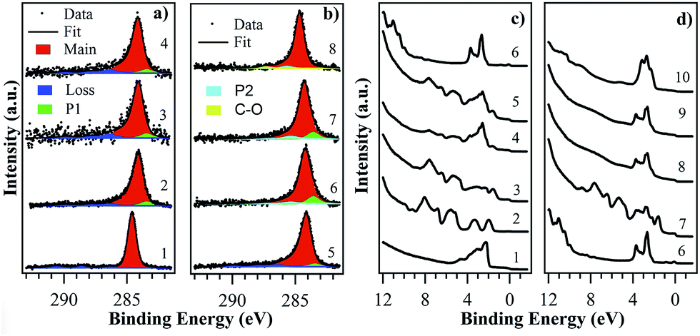 | ||
| Fig. 1 (a) C 1s CL from C60 film deposited at RT by SuMBE on Cu poly at KE = 15 eV (1, 2) and Cu(111) at KE = 35 eV (3, 4) with thickness: (1) 20 nm; (2) 1ML, after annealing 20 nm film at 400 °C; (3) 0.3ML; (4) 0.6ML. (b) C 1s CL from C60 1ML films deposited at RT for precursor KE = 35 eV, after thermal annealing at 425 °C (5), 645 °C (6), 795 °C (7). C 1s emission from commercial graphene single-layer on Cu foil is shown for comparison (8). (c) VB from Cu poly (1); VB analysis of C60 films deposited by SuMBE on Cu poly at RT for KE = 15 eV (2, 3) and Cu(111) at KE = 35 eV (4, 5) with thickness: (2) 20 nm; (3) 1ML, after annealing a 20 nm film at 400 °C; (4) 0.3ML; (5) 0.6ML. (d) VB from Cu(111) (6); VB from C60 1ML film deposited at RT with KE = 35 eV, after thermal annealing at 425 °C (7), 645 °C (8), 795 °C (9). VB from a commercial graphene single-layer on Cu foil (10) is shown for comparison. | ||
Valence band (VB) in Fig. 1c(2) is dominated by several features, with the highest occupied molecular orbital (HOMO) being located at ∼2 eV. We evaluated from UPS analysis a work function (WF) of 4.80 eV, with an ionization potential (IP) of 6.5 eV. The C60 1 monolayer (1ML) was obtained by annealing the 20 nm C60 film at 400 °C on a Cu poly, removing all physisorbed species.
C 1s CL analysis shows an asymmetric main peak (Fig. 1a(2)) located at 284.14 eV (FWHM 0.92 eV, 87%), a component labeled P1 in Fig. 1a at 283.44 eV (FWHM 1.00 eV, ∼3%) and the presence of loss structures at higher BEs. Additionally, the same ∼−0.45 eV BE shift and band enlargement as for the C60 20 nm film can be found in VB spectrum (Fig. 1c(3)). Copper 3d bands intensity is decreased with respect to clean surface (Fig. 1c(1)), while main features and Fermi edge are still visible. The WF is ∼5.0 eV, higher than for Cu surface (WF ∼ 4.8 eV) and thick C60 film. These C 1s CL features (BE, width and weight) can be found even in C60 1ML films deposited at RT by SuMBE at 15 and 35 eV precursor KEs on substrates of Cu poly/Cu(111) (Fig. S1 and S2 of the ESI†).
VB spectra show differences only related to the copper substrate (Fig. S3 of the ESI†), and the WF is the same for the C60 1ML on Cu(111), with a small ∼0.1 eV increase from the clean surface (WF = 4.94 eV).
The observed C 1s peak asymmetry and energy shifts are attributed to charge transfer from the metallic substrate to the C60 ML in a chemisorption process.37–39 At variance with MBE deposition, the C 1s CL lineshape recorded after SuMBE is not reproducible via a simple Doniach–Sunjic profile and a new peak (P1) has to be introduced to fit properly the data.37 This feature, while has never been observed in the 1ML C60/Cu(111) system, was found in C60 on Ta(110) and related to charge transfer.40,41 The −0.7 eV separation in BE between P1 and the main peak is typical of covalent bond formation, as for C60 on Si.17 However, this has to be excluded in the case of C60 on copper.
The P1 peak, located at BE lower than expected for graphene on copper,42 could be instead interpreted as the fingerprint of cage rupture, induced in the C60 high impact collision on Cu and leading to free-standing graphene flake formation on the surface. Therefore, if this interpretation was correct, the presence of P1 would suggest an energy threshold for cage opening at about 15 eV. Nevertheless, the P1 peak intensity did not show appreciable changes in RT deposition of C60 on Cu at 15 eV or 35 eV initial beam KE, a surprising indication that C60 unzipping is not improved by doubling precursor KE.
To rule out the presence of P1 in the spectrum as a fingerprint of cage rupture, we deposited 0.3ML and 0.6ML C60 films on Cu(111) at 35 eV KE, as low coverage and high KE represent the conditions for which C60 cage rupture would most likely occur. From C 1s CL analysis (Fig. 1a(3 and 4)), P1 represents always ∼3–4% of the total C 1s area, while VBs differ only for C60 features intensity (Fig. 1c(4 and 5)). Thus, P1 peak can be safely attributed to copper-to-carbon charge transfer leading to the conclusion that experimental evidence of cage breaking towards graphene formation upon C60 impact at these kinetic energies cannot be found. Unfortunately, 35 eV is the highest C60 KE attainable by SuMBE deposition in our experimental apparatus; thus, one has to rely on ab initio simulations to find such KE threshold for cage rupture and to further investigate the chemical–physical processes occurring during the impact of fullerene with a Cu(111) surface.
3.2 Born–Oppenheimer DFT and non-adiabatic molecular dynamics simulations
We performed simulations of C60 impact on Cu(111) surfaces, with a series of initial kinetic energies in the range 70–210 eV using DFT (Fig. 2a). In a previous work, concerned with SiC growth induced by SuMBE of C60 on Si(111), we demonstrated that substrate temperature has very limited effect on cage breaking mechanisms.43 Thus, we decided to perform DFT simulations at RT. Details on these simulations and the parameters used are given in Section 2.2.1. The results of these calculations showed no cage breakup for initial kinetic energies of 70 and 100 eV, whereas breakup was obtained at 210 eV. We notice that this value is comparable to the estimation of breakup threshold energy based on the average C–C dissociation bond energy (∼4 eV per bond44) which would result in a 360 eV threshold for full C60 breakup. A movie of the full trajectory with this initial C60 kinetic energy is available as ESI.†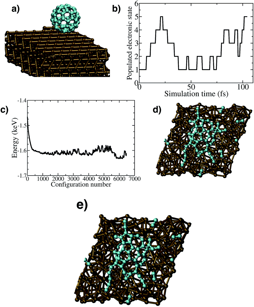 | ||
| Fig. 2 (a) C60 impinging on Cu(111) surface. (b) Excited electronic states visited during a TD-DFT simulation of C20 impinging on Cu(111) surface at 14 eV (corresponding to C60 at 42 eV) (c) C20 final configuration after cage breaking on Cu(111) surface. (d) Total electronic energy of the system during a metadynamics simulation starting from the configuration of a broken C60 cage on Cu(111) surface. (e) Final configuration of the metadynamics-DFT simulation. | ||
This energy scale is well beyond the experimental kinetic energies of SuMBE approach. However, these simulations rely on the validity of the Born–Oppenheimer (BO) approximation, assuming that ionic and electronic motions proceed on decoupled timescales.
In C60, the 1.6 eV band-gap corresponds to emission in the frequency region of 1015 Hz, and the collisional time scale in our case – as estimated using BO-DFT calculations – is of the order of few tens of femtoseconds (≃1014 Hz). The ratio between nuclear (τp) and electronic characteristic times (τe) is of the order of τp/τe ≃ 1–10, thus non-adiabatic effects can be expected to be significant in this case. Unfortunately, a full treatment of electronic excitations is infeasible for the C60/copper system used in BO-DFT simulations. Therefore, we decided to use a non-adiabatic molecular dynamics (NAMD) approach with C20 as impinging molecule by reducing accordingly the initial KE (1/3 of C60).16 We notice that the principal differences between C20 and C60 are: the HOMO–LUMO energy (0.54 eV vs. 1.64 eV respectively) and the cohesive energy per carbon atom (6.26 eV per atom vs. 7.15 eV per atom respectively). This indicates that the rupture threshold per atom calculated using C20 can represent a lower bound to the C60 results. We performed three simulations of C20, with initial kinetic energies of 14, 8, and 5 eV (corresponding to 42, 32, and 15 eV for C60 having the same initial velocity) to find the kinetic energy threshold. Each simulation lasted 0.2 ps with a time-step of 0.5 fs. The fragmentation of the cage happened only in the first case, while it was not obtained in the other two. As a check, we also performed a BO-DFT simulation of C20 impact at an initial kinetic energy of 14 eV, and we did not observe fragmentation, enforcing once more the role of electronic excited states on the cage breaking. The threshold for complete cage breaking is found at 14 eV (corresponding to 42 eV for the equivalent problem of C60) confirming our experimental evidence of a C60 rupture KE threshold higher than that attainable by SuMBE. However, large distortions of the C60 cage and surface penetration can be found already for KE = 30 eV. As a check, we also performed a BO-DFT simulation of C20 impact on Cu at an initial kinetic energy of 14 eV and we did not observe the fragmentation, enforcing once more the role of the electronic excitations on the cage breaking.
We report in Fig. 2b the excited states instantly visited by a C20 molecule impinging on the Cu(111) surface. At C–Cu distance below 2.5 Å (around 20 fs) highly excited energy surfaces become progressively populated until the cage breaks, as is evident in the last frame of the trajectory, reported in Fig. 2c.
We conclude that, analogously to what has been observed in the impact of fullerenes on silicon, a model including excited electronic states is necessary to describe accurately the KE threshold of carbon cage rupture, as BO ground-state DFT is in error by a factor of 5. A movie of the fullerene trajectory all the way from the initial condition to breaking is reported in the ESI.† There, one can clearly observe fragmentation of C20 impinging with a kinetic energy of 14 eV on the Cu(111) surface on a timescale spanning 104 fs.
The kinetic energy threshold for projectile breaking can in principle be estimated also by a continuum mechanical model (CM).45 The kinetic energy threshold for projectile breaking in a CM is assumed proportional to the object volume V, where the proportionality constant is the product of the mechanical strength of the projectile and the ratio of the projectile and target densities.45 The threshold velocity v for breakup at temperature T would then be given by:
 | (1) |
3.3 LEED analysis
From both our experimental and computational investigations, one should rule out the possibility of a complete disruption of the cage at the KE achievable by SuMBE of C60 on copper. One route to follow could be to change the projectile, as a larger mass would result in a higher KE. However, larger mass fullerenes, such as C120, are less abundant and more expensive than C60 within the fullerene family. Thus we decided to look for a possible solution by increasing the substrate temperature.In order to evaluate the possible thermally induced C60 unzipping we deposited a C60 1ML film at 35 eV KE on Cu(111) at RT. A thermal annealing sequence in the range 107–795 °C (see Section 2.1.3) has been systematically performed.
Furthermore, C 1s CL, VB and LEED pattern have been measured, looking for any modifications of C60 1ML film properties at each temperature. LEED analysis revealed a diffuse background up to 425 °C, when a complex pattern for the 1ML film appeared (Fig. 3b), with several extra-spots superimposed to the original Cu(111) features (Fig. 3a). The appearance of these signals can be interpreted as a rearrangement of the C60 molecules on Cu(111) surface in a 4 × 4 superstructure,46 made favourable by the very low mismatch (∼2%) between the lattice parameter of the organic crystal (10.02 Å) and of the quadruple value of Cu (10.24 Å). This system, characterised by a charge transfer from Cu and C60 rotation, undergoes a reconstruction in which a seven atom cavity is formed in the first copper layer, where a single C60 cage can be hosted.47–50
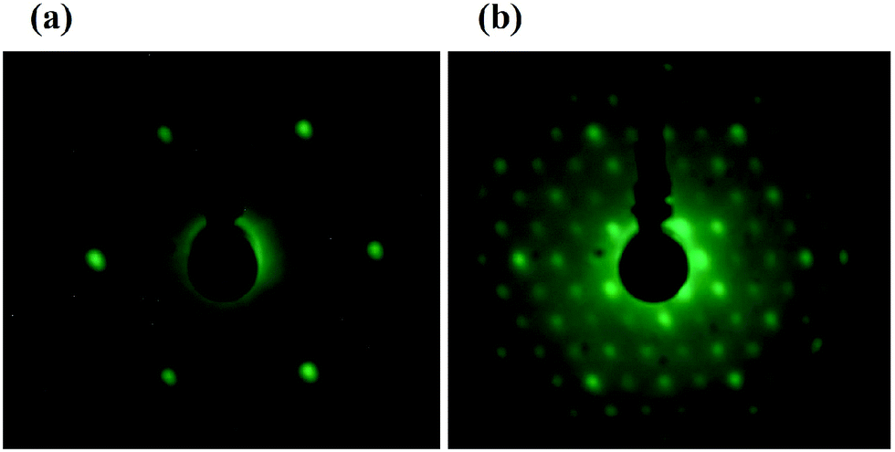 | ||
| Fig. 3 LEED pattern (70 eV) for a clean Cu(111) surface (a) and for 1ML C60/Cu(111) (b) after annealing of a 20 nm thick film at 425 °C. | ||
A quarter of the entire C60 molecule can be accommodated in this cavity and, thus, is found at short distance from 12 copper atoms,47–50 leading to the observed chemisorption process and charge transfer from C60 to Cu(111) surface. A similar metal surface reconstruction was found in C60/Ru(0001) adsorption47–50 where Ru–C strong interaction within the cavity leads to a distortion of C60 bonds, to cage opening within the fault line at high temperature and, eventually, to the creation of graphene quantum dots.7
3.4 Core-level characteristics of the thermally-assisted SuMBE grown graphene
In light of both 4 × 4 relaxation pattern and metallic substrate reconstruction it is tempting to relate the C 1s P1 peak appearance in CL spectra (Fig. 1a(2–5)) with the carbon atoms experiencing the shortest distance from Cu (despite showing some features typical of C60 1ML as in MBE deposition).While simulations predict cage rupture KEs out of reach by SuMBE (>42 eV), however NAMD simulations pointed out that already in the 15 to 35 eV KE range collisions induce cage distortion and significative surface penetration. We note that this process takes place during RT deposition and before the 4 × 4 C60 rearrangement on the surface, occurring only at temperatures of 100 °C higher than those used in MBE deposition (where C60 remains intact on copper due to the low KE reached). This means that carbon atoms are in tight contact with the copper surface and much energy has to be spent to diffuse and rearrange the C60 cages, partially deformed or in close contact with copper within the surface cavities.
Chemical properties from C 1s CL and VB remain unchanged up to 645 °C (Fig. 1b(6), where C 1s CL showed a −10% intensity reduction and deep lineshape change. A comparison with the 1ML CL (Fig. 1b(5)) shows that the main peak is larger (FWHM +0.1 eV), located at higher BE (+0.1 eV) and characterised by a different asymmetry with a typical Doniach–Sunjic lineshape. Furthermore, the previously observed loss structure is absent, the P1 peak is more intense (∼8%) and it shows the same energy shift of the main component. A new weak component (P2, Fig. 1b(6)) is present at 285.35 eV (FWHM ∼ 1.25 eV, ∼3–4%). These features are typical of a defected graphene single-layer.51 C 1s CL analysis from a commercial graphene single-layer on a copper foil (Fig. 1b(8)) is characterised by a main peak located at 284.65 eV (FWHM 0.88 eV), a peak at 285.65 eV (P2, FWHM 1.00 eV) and a further component at 287.40 eV (FWHM 1.30 eV) due to presence of C–O bonds. Thus, apart from a +0.1 eV shift and lower peak broadening, C 1s CL suggests we have synthesised a graphene single-layer, revealing the presence of some defects as evidenced by the larger width and very intense P2 peak.51
A second demonstration, increasing our confidence that a stable graphene sheet has been grown, is provided by VB analysis. VB curves (Fig. 1d(8)) indeed have lost the typical C60 features, showing only the Cu 3d band and two broad features in the 6–9 eV region, which is a clear indication of cage rupture occurrence. Furthermore, no significant changes (for C 1s CL and VB) were observed up to 795 °C (Fig. 1b(7) and d(9)). From the attenuation of Cu 2p peak we can evaluate the film thickness before and after the thermal treatment at 645 °C. We find that the thickness profile changes from 0.9 nm to 0.46 nm, which represents a decrease from the typical value found in 1ML of C60 towards the nominal thickness of a single layer of graphene.52
It is worth noting the absence of oxidized species in our film, owing to both SuMBE approach and to the use of C60 as precursor. Finally, our electron spectroscopy analysis, in agreement with that of standard films grown by CVD, can hardly reveal the presence of graphene. Furthermore, a clear LEED pattern, differently from what we obtained for the 4 × 4 C60 reconstruction, was not found indicating the presence of a material with a small coherent length (less than 20 nm) that hinders the formation of LEED diffraction.
3.5 Metadynamics simulations
To demonstrate that upon fullerene cage unzipping and thermal treatment carbon atoms reorder in a graphene-like arrangement, we performed first-principles simulations on timescales much longer than those accessible with ab initio molecular dynamics. To accelerate the dynamics of atomic carbons moving and reacting on the copper surface, one must use methods able to sample efficiently the configuration space, notably Kinetic Monte Carlo (KMC, see e.g. ref. 26 for a discussion on graphene growth on copper) or metadynamics36 (see Section 2.2.3 for details). However, KMC requires the calculations of all possible transition rates occurring at the carbon–copper interface. This is a very complex task to be reached by means of ab initio simulations owing to the complexity of the transition patterns with a large number of atoms (e.g. carbon diffusion on the surface, formation of carbon dimer, trimer and other possible clusters, etc.…), thus we decided to use metadynamics.We do not expect excited state dynamics to be significant in the rearrangement of C atoms on the Cu surface. In fact, once the cage is broken, dissipation processes will begin to play a significant role and light electrons will quickly relax to their ground state (for a given position of the nuclei). The subsequent nuclear relaxation, leading to C atoms rearrangement, will therefore be mostly determined by the ground-state electronic surface. Thus, the system dynamics can be describe within the BO approximation.
Upon C60 cage rupture on top of a Cu(111) surface, by following the metadynamics evolution of our system, we find a pronounced tendency of carbidic clusters to rearrange into graphene-like networks. Our metadynamics simulation shows in particular that the number of C–C bonds increase from ∼40 to 60. This trend is accompanied by a significant decrease in the electron energy – see Fig. 2d – which indicates the exploration of progressively lower energy states.
The very high computational cost of performing metadynamics simulations prevented us to go beyond ∼6000 BO steps. Nevertheless, even this time-limited dynamics indicates clearly the tendency of a broken C60 cage on Cu(111) towards rearranging in a graphene-like network. We note that carbon molecules are hosted within the defected and terraced Cu(111) surface. In particular, we show in Fig. 2e the last frame of our metadynamics simulation, where one can see the presence of 3 hexagons and a Stone–Wales defect (made by a pentagon and a heptagon). Comparison with similar calculations starting from C20 broken cages, where no tendency to form graphene was observed, indicates that the formation of graphene needs a sufficiently high density of carbon atoms on the surface. A full trajectory movie of our metadynamics simulation is attached to the ESI.†
3.6 SEM/STM analysis of the samples
SEM and STM ex situ analysis revealed the presence of terraces (Fig. 4a), typical of Cu(111) surface. High resolution STM images (Fig. 4b) show a graphene lattice, presenting dark point defects and bright contrast lattice distortion, separating few nm extended graphene-like domains as confirmed by Fast Fourier Transform (FFT) analysis of the STM data (Fig. 4e). These results suggest the presence of defected single layer graphene, with a small coherent length that hinders the formation of LEED diffraction. | ||
| Fig. 4 C60 1ML on Cu(111) after annealing at 645 °C. SEM (a) and STM (b–e) analysis. (c) Details of a dark region, with line profile (d); (e) FFT analysis of the image in (b). | ||
Nevertheless, the recognition of single-layer versus multilayer graphene could not be achieved by STM images only, owing to substrate–graphene interaction and Moiré effects on hexagonal fcc (111) substrates that could influence the contrast of the graphene lattice. This effect has been already reported by Gao and coworkers53 on single-layer graphene grown on polycrystal Pt. In this work, different electronic contrast patterns were observed depending on the exposed Pt facet. In particular, for the (111) facets the graphene overlayer shows an hexagonal lattice with a carbon-to-carbon bond length of 2.46 Å, as observed in graphite, at odds with the expected 1.42 Å bond length of graphene. Similar observations were reported by Sicot et al. for graphene on the top of Rh(111).54 Finally, for CVD-grown graphene on Pt(111) full graphene lattice was indeed observed for (2 × 2) and (3 × 3) Moiré domains.55
The graphene flake dimensions and high density once more substantiate our view of thermally-assisted unzipping of C60 molecules arranged on the top of Cu(111) surface due to the SuMBE deposition. Dark region line profile reveals a depth of ∼2 Å and a width of ∼1 nm (Fig. 4c and d). As Cu(111) interlayer distance is 2.06 Å, dark regions are compatible with the formation of fault lines on the top of the metal representing the C60 adsorption sites, which, as mentioned before, are created by a seven atom vacancy. Once unzipped, the bottom part of the cage remains inside the first layer, being responsible for the P1 peak signal in CL spectra of our system, still present after graphene synthesis (Fig. 1b(6 and 7)).
3.7 Raman analysis of the samples
The ultimate evidence for demonstrating graphene synthesis is given by Raman analysis. As shown in Fig. 5A, spectra from three different regions are characterised substantially by the same features, dominated by the D (A1g mode), G (E2g mode) and 2D (second order Raman scattering process in curved graphene) bands at 1349, 1589 and 2665 cm−1, respectively. G band is biphasic and is formed by a second D′ component at 1624 cm−1.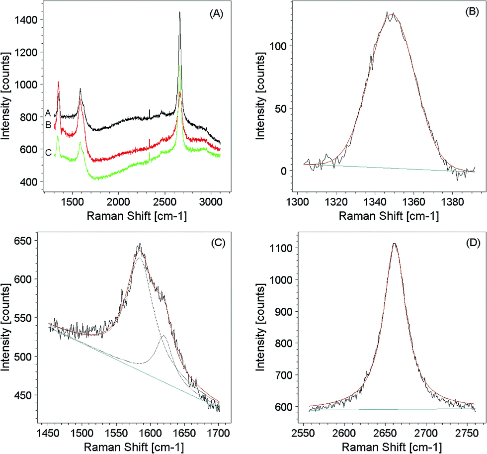 | ||
| Fig. 5 Micro Raman analysis of C60 1ML on Cu(111) after annealing at 645 °C. (A) Wide-view Raman spectra acquired in different regions of the sample. (B) High resolution D band, (C) high resolution G + D′ and (D) 2D bands acquired on the same sample, together with their Lorentzian peak fitting. | ||
The G band originates from a normal first order Raman scattering mediated by TO and LO phonons. Because in these processes the transitions connect points around the same K Dirac point, they are called intervalley processes.56 The D and 2D-bands originate from a double resonance process, involving one TO phonon and one defect in the case of the D-band or two TO phonons for the 2D band. Since these processes involve states around two distinct K and K′ Dirac points are called intravalley processes. Similarly to the D band, the less intense D′ band originates from a double resonant process involving one defect and one phonon but now the transitions are located only around the K point in an intervalley process (for more details see ref. 56).
A minor peak is found at ∼2400 cm−1 (Fig. 5A). This can be assigned to the G* band,57 while at ∼2470 cm−1 appears a weak feature usually associated to the D + D′′ band.58 Again, D + D′ band is visible at ∼2900 cm−1.59
The latter features can be associated to the presence of a certain degree of disorder in our single-layer graphene. The G* band can be explained by an inter-valley process involving one TO and one LA phonon, typically present in the acoustic and optical phonon dispersion of graphene. Finally a sharp feature appears at ∼2330 cm−1. A similar feature was observed by Pimenta et al.60 in disordered graphite and was attributed to Raman band associated with the N–N stretching mode (Q band, ΔJ = 0) of N2 molecules present in the air surrounding the sample or adsorbed on the sample surface.61
The main difference between the two couples (G, 2D) and (D, D′) Raman components is that G and 2D bands originate from a classic Raman scattering process involving one and two phonons respectively. D and D′ bands are double resonant processes which involve one phonon and one defect. For this reason, comparison between intensities (integrated areas) of the bands belonging to the first and second Raman peaks is used to gain information related to the material's disorder degree. In this respect, the I(D)/I(G) intensity ratio is considered as a good parameter to assess the defect density. In particular, a strong increase of the I(D)/I(G) ratio can be found moving from crystalline to polycrystalline graphite characterized by a high number of defects (example of this approach can be found in the work by Ferrari et al.,62 describing the “amorphization trajectory” of I(D)/I(G) and the changes of the G band position going from pure crystalline to polycrystalline graphite and to amorphous carbons with different percentages of sp2 sp3 hybrids).
A similar analysis can be applied to the graphene islands grown by SuMBE. A first important information is gained by fitting the D and G bands (Fig. 5B and C). Generally, a Lorentzian lineshape describes accurately the G and D peaks also in disordered graphite, and the finite lifetime broadening as in typical Breit–Wigner–Fano (BWF) processes.62 However, the increase in lifetime broadening due to increasing material disorder leads to a more pronounced Gaussian behaviour, as reported in Fig. 5B.
The I(D)/I(G) ratio for regions A, B and C amounts to 0.71, 1.07 and 0.84 respectively, revealing the presence of a certain degree of disorder. This disorder can be identified by irregularities of the single-layer graphene obtained by SuMBE, such as the presence of pentagons and vacancies. All these defects are characterized by a strong degree of localization. In the case of point defects, Lucchese et al.63 proposed a simple relation linking the defect density generated by ion irradiation to the I(D)/I(G) ratio as:
| I(D)/I(G)(Ld) = CAfA(Ld) + CSfS(Ld) | (2) |
| I(D)/I(G)(Ld) = (102 ± 2)/Ld2 | (3) |
Using the I(D)/I(G) ratio measured in our samples, we can estimate an average defect-to-defect distance of about 18.4 ± 2, 15.6 ± 2 and 16.8 ± 2 nm, in agreement with the hypothesis of low concentration of point defects. To demonstrate that the Raman spectra measured on our samples grown via SuMBE give a clear indication of the presence of graphene with some degree of crystallinity, we compare our results with those obtained by Chua et al. and Lu et al.64,65 where graphene growth was reached starting from fullerenes. These Raman spectra do not show a 2D Raman component as distinctive sign of graphene-like structures. Further evidence of graphene growth by SuMBE can be obtained by comparing our measured spectra with those obtained by Wang et al.66 In this work, fullerene-like structure were synthesised starting from amorphous aC–H matrix. The Raman spectra of this material show rather broad features and D, G, D′ bands are hardly recognizable, leading again to the conclusion that SuMBE is a very promising technique to synthesize graphene domains characterized by good crystalline structure despite the presence of some defects.
In addition to defect analysis, the I(D)/I(G) ratio can be used to estimate the dimension of graphene domains. This is a consequence of the proportionality of I(D)/I(G) to the number of ordered hexagons in graphene, assuming that the D peak intensity depends on phonon confinement. In this regard, the effect of disorder may be considered as a decrease in number of ordered rings.62 The planar graphitic domain size La can be then assessed, as proposed by Tuinstra et al.,67 by:
| I(D)/I(G) = C(λ)/La | (4) |
While this relation was initially developed for the assessment of the Raman spectrum of graphite, however has been after successfully used for graphene.62,68,69 The coefficient C(λ) depends on the excitation wavelength and is about 4.4 nm for a 514.5 nm excitation wavelength.70 For higher wavelengths, such as the 633 nm laser used, one can refer to the work of Cançado71 where the I(D)/I(G) ratio is assessed by area integration and a value of C(λ) = 38.53 nm is obtained by fitting the following formula:
| C(λ) ≃ 2.4 × 10⁻¹⁰λ4 | (5) |
By using eqn (3) is possible to estimate graphene crystalline domain sizes, which result equal to 128.2, 91.7, and 106.4 nm, respectively.
The modulation of the 2D/G peak intensity is equal to 3.07, 1.59, 3.87 for regions A, B, C, respectively (Fig. 5A). A decrease in I2D/IG ratio reflects energy dispersion through larger number of channels, i.e. a high degree of non-crystalline phases. Indeed, the introduction of disorder through high energy electron beam irradiation of graphene leads to different trends of ID/IG and I2D/IG intensities.61 In particular, in the low disorder regime, ID/IG increases while the opposite trend can be found at high dose of energetic electrons (high disorder regime). Differently, the I2D/IG ratio assumes a descending trend from the initial irradiation stages revealing insensitivity to the high/low disorder regimes.
Finally, it is known that structural information on graphene, in particular the presence of single- or multi-layers, is reflected by 2D features. In our case, the G + D′ and 2D features were fitted to follow changes in their morphology by changing the acquisition regions (A, B and C) of the sample surface. An example of fit performed in region A is shown in Fig. 5B and C. Only a Lorentzian component is needed to fit the 2D peak (Fig. 5D). This information along with the 2D lineshape visible symmetry leads us to the conclusion that we are indeed analysing single-layer graphene.
FWHM typical value for the 2D Lorentzian component in a pure graphene monolayer is about 24 cm−1.56 In our A, B, and C regions, the FWHM values are equal to 30, 50 and 33 cm−1. These values are in good agreement with those obtained by Wang et al.72 where the FWHM of the graphene 2D component ranges from 30 to 59 cm−1, depending on substrate type. The higher FWHM corresponds to a SiC substrate to which graphene adheres strongly. This leads to a shift of the G and 2D Raman bands, not present in any of our samples. This information along with the 2D symmetric profile leads us to the conclusion that in the cases A and C we are indeed analyzing single-layer graphene, in agreement with a lower I(2D)/I(G) ratio. For the sample B, the higher FWHM could be partially explained by a higher defect density. The presence of a layered structure cannot be excluded, although this occurrence should result in a different lineshape.56,70
4 Conclusions
In this work, we report single-layer graphene growth by thermal decomposition of C60 films deposited by SuMBE on Cu(111) surfaces. To the best of our knowledge, while MBE thermal decomposition of graphitic layers was already achieved,73–77 a defected but uniform single-layer graphene film from C60 has never been synthesized on surfaces showing low chemical interaction with fullerene. This was only achieved for nickel and ruthenium, at process temperatures considerably higher than those used in our experiment.The SuMBE approach, inducing a tighter C60 interaction with the copper surface, creates favorable conditions for cage unzipping via thermal processes with respect to other widely used approaches. C60 cage opening, in particular, was not achieved at the KEs attainable by SuMBE, in agreement with non-adiabatic molecular dynamics simulations, predicting breaking well above 40 eV. However, cage unzipping has been obtained by thermal treatment of C60 deposited by SuMBE, after a reconstruction of the surface allowing for an effective molecular orbital/metal valence states overlap. We note that we observed graphene synthesis by SuMBE already at 645 °C, a temperature significantly lower than those attainable by CVD.
The possibility to control cage rotation, supra-molecular organization and unzipping process on Cu surface is promising for the reduction of defects in the graphene layer, through a coherent matching of the different flakes originating from C60. Nevertheless, the presence of a defected hexagon networks in SuMBE grown graphene, as shown by our STM and Raman analysis and predicted by long-time metadynamics simulations, could be interesting for micro-electronic applications, where a band gap has to be induced in graphene, and to study penta-graphene, a new carbon allotrope recently proposed in theoretical studies.78 Moreover, defects in graphene, as well as introduction of dopants and modification of the surface by metal/metal oxide nanoparticles, could promote the use of this material for gas sensors.79
Theoretical calculations already demonstrated that introduction of dopants and defects in graphene improves the sensitivity of graphene-based gas sensors,80 in particular transition metal dopants (Co, Fe) lead to an higher affinity towards selected molecules (H2S) compared to pristine graphene.81
Finally, we envisage that graphene synthesis could be induced at RT also during the molecule/surface high impact collision on copper by introducing some impurities on the surface to avoid that the excess of kinetic energy made available by SuMBE is spent in molecular diffusion on the surface rather than in cage breaking. Furthermore, we devise that our approach can be used to synthesize graphene on substrates different from copper, for example directly on semiconductors at a temperature much lower than graphene growth on SiC, and, due to the collimated nature of the beam in SuMBE, in an unprecedented region-selective modality.
Acknowledgements
We acknowledge funding from the EU under the FP7th grant agreement 604391 (Graphene Flagship), from FBK via the CMM Director grant “SuperCar”, and PRIN project DESCARTES (no. 2010BNZ3F2), MIUR, Italy. N. M. P. is supported by ERC StG Ideas 2011 BIHSNAM (no. 279985), ERC PoC 2013-1 REPLICA2 (no. 619448), and by ERC PoC 2013-2 KNOTOUGH (no. 632277). S. T., N. M. P. and G. G. are also supported by the Provincia Autonoma di Trento (“Graphene nanocomposites”, no. S116/2012-242637 and reg. delib. no. 2266). G. G. and S. T. acknowledge support by INFN through the “Supercalcolo” agreement with FBK. S. T. gratefully acknowledges the Institute for Advanced Studies in Bologna for supporting his ISA fellowship. We thank Prof. D. Alfè (UCL), Dr S. a. Beccara (ECT*), and Dr M. Dapor (ECT*) for invaluable discussions on simulation topics. Computer simulations were performed on the Archer Supercomputing Facilities (UK) and on the KORE computing cluster at FBK. R. V. thanks L. Gavioli (Università Cattolica) for his support in SEM/STM analysis, and C. Corradi and M. Pola for their technical assistance.References
- H. Tetlow, J. P. de Boer, I. Ford, D. Vvedensky, J. Coraux and L. Kantorovich, Phys. Rep., 2014, 542, 195–295 CrossRef CAS.
- D. Haberer, D. V. Vyalikh, S. Taioli, B. Dora, M. Farjam, J. Fink, D. Marchenko, T. Pichler, K. Ziegler, S. Simonucci, M. S. Dresselhaus, M. Knupfer, B. Büchner and A. Grüneis, Nano Lett., 2010, 10, 3360–3366 CrossRef CAS PubMed.
- R. Muñoz and C. Gómez-Aleixandre, Chem. Vap. Deposition, 2013, 19, 297–322 CrossRef.
- Z. Yan, Z. Peng and J. M. Tour, Acc. Chem. Res., 2014, 47, 1327–1337 CrossRef CAS PubMed.
- E. S. Penev, V. I. Artyukhov, F. Ding and B. I. Yakobson, Adv. Mater., 2012, 24, 4956–4976 CrossRef CAS PubMed.
- S. D. Leifer, D. G. Goodwin, M. S. Anderson and J. R. Anderson, Phys. Rev. B: Condens. Matter Mater. Phys., 1995, 51, 9973–9978 CrossRef CAS.
- J. Lu, P. S. E. Yeo, C. K. Gan, P. Wu and K. P. Loh, Nat. Nanotechnol., 2011, 6, 247–252 CrossRef CAS PubMed.
- L. M. Peridigão, S. N. Sabki, J. M. Garfitt, P. Capiod and P. H. Beton, J. Phys. Chem. C, 2011, 115, 7472–7476 Search PubMed.
- A. V. Talyzin, S. Luzan, I. V. Anoshkin, A. G. Nasibulin, E. I. Kauppinnen, A. Dzwilewski, A. Kreta, J. Jamnik, A. Hassanien, A. Lundstedt and H. Grennberg, J. Phys. Chem. C, 2014, 118, 6504–6513 CAS.
- O. Chernogorova, I. Potapova, E. Drozdova, V. Sirotinkin, A. Soldatov, A. Vasiliev and E. Ekimov, Appl. Phys. Lett., 2014, 104, 043110 CrossRef.
- C. K. Chua, Z. Sofer, P. Šimek, O. Jankovský, K. Klímová, S. Bakardjieva, Š. Hrdliçková Kučková and M. Pumera, ACS Nano, 2015, 9, 2548–2555 CrossRef CAS PubMed.
- C. Tiwary, B. Javvaji, C. Kumar, D. Mahapatra, S. Ozden, P. Ajayan and K. Chattopadhyay, Carbon, 2015, 89, 217–224 CrossRef CAS.
- M. C. Paiva, W. Xu, M. F. Proença, R. M. Novais, E. Laegsgaard and F. Besenbacher, Nano Lett., 2010, 10, 1764–1768 CrossRef CAS PubMed.
- R. N. Tiwari, M. Ishihara, J. N. Tiwari and M. Yoshimura, Chem. Commun., 2012, 48, 3003–3005 RSC.
- S. Ozden, P. A. S. Autreto, C. S. Tiwary, S. Khatiwada, L. Machado, D. S. Galvao, R. Vajtai, E. V. Barrera and P. M. Ajayan, Nano Lett., 2014, 14, 4131–4137 CrossRef CAS PubMed.
- S. Taioli, G. Garberoglio, S. Simonucci, S. A. Beccara, L. Aversa, M. Nardi, R. Verucchi, S. Iannotta, M. Dapor and D. Alfè, J. Chem. Phys., 2013, 138, 044701 CrossRef PubMed.
- R. Verucchi, L. Aversa, M. V. Nardi, S. Taioli, S. A. Beccara, D. Alfè, L. Nasi, F. Rossi, G. Salviati and S. Iannotta, J. Am. Chem. Soc., 2012, 134, 17400–17403 CrossRef CAS PubMed.
- M. Nardi, R. Verucchi, R. Tubino and S. Iannotta, Phys. Rev. B: Condens. Matter Mater. Phys., 2009, 79, 125404 CrossRef.
- G. Kresse and J. Hafner, Phys. Rev. B: Condens. Matter Mater. Phys., 1993, 47, 558–561 CrossRef CAS.
- G. Kresse and J. Hafner, Phys. Rev. B: Condens. Matter Mater. Phys., 1994, 49, 14251–14269 CrossRef CAS.
- G. Kresse and J. Furthmüller, Comput. Mater. Sci., 1996, 6, 15–50 CrossRef CAS.
- G. Kresse and D. Joubert, Phys. Rev. B: Condens. Matter Mater. Phys., 1999, 59, 1758–1775 CrossRef CAS.
- P. E. Blöchl, Phys. Rev. B: Condens. Matter Mater. Phys., 1994, 50, 17953–17979 CrossRef.
- J. P. Perdew and A. Zunger, Phys. Rev. B: Condens. Matter Mater. Phys., 1981, 23, 5048–5079 CrossRef CAS.
- J. P. Perdew, K. Burke and M. Ernzerhof, Phys. Rev. Lett., 1996, 77, 3865–3868 CrossRef CAS PubMed.
- S. Taioli, J. Mol. Model., 2014, 20, 1–13 CrossRef CAS PubMed.
- D. Alfè, Comput. Phys. Commun., 1999, 118, 31–33 CrossRef.
- M. Barbatti, Wiley Interdiscip. Rev.: Comput. Mol. Sci., 2011, 1, 620–633 CrossRef CAS.
- J. C. Taylor, Phys. Rev., 1954, 95, 1313–1317 CrossRef.
- N. Troullier and J. L. Martins, Phys. Rev. B: Condens. Matter Mater. Phys., 1992, 46, 1754–1765 CrossRef CAS.
- D. M. Ceperley and B. J. Alder, Phys. Rev. Lett., 1980, 45, 566–569 CrossRef CAS.
- L. D. Landau, Physics of the Soviet Union, 1932, 2, 28 Search PubMed.
- C. Zener, Proc. R. Soc. London, Ser. A, 1932, 137, 696–702 CrossRef.
- D. Marx and J. Hutter, Ab Initio Molecular Dynamics: Basic Theory and Advanced Methods, Cambridge University Press, Cambridge, 1st edn, 2009, vol. 4 Search PubMed.
- W. Andreoni and A. Curioni, Parallel Computing, 2000, 26, 819–842 CrossRef.
- A. Laio and F. L. Gervasio, Rep. Prog. Phys., 2008, 71, 126601 CrossRef.
- K.-D. Tsuei, J.-Y. Yuh, C.-T. Tzeng, R.-Y. Chu, S.-C. Chung and K.-L. Tsang, Phys. Rev. B: Condens. Matter Mater. Phys., 1997, 56, 15412–15420 CrossRef CAS.
- A. Tamai, A. P. Seitsonen, F. Baumberger, M. Hengsberger, Z.-X. Shen, T. Greber and J. Osterwalder, Phys. Rev. B: Condens. Matter Mater. Phys., 2008, 77, 075134 CrossRef.
- B. W. Hoogenboom, R. Hesper, L. H. Tjeng and G. A. Sawatzky, Phys. Rev. B: Condens. Matter Mater. Phys., 1998, 57, 11939–11942 CrossRef CAS.
- D. Tománek, W. Zhong and E. Krastev, Phys. Rev. B: Condens. Matter Mater. Phys., 1993, 48, 15461–15464 CrossRef.
- P. Rudolf and G. Gensterblum, Phys. Rev. B: Condens. Matter Mater. Phys., 1994, 50, 12215–12217 CrossRef CAS.
- P. R. Kidambi, B. C. Bayer, R. Blume, Z.-J. Wang, C. Baehtz, R. S. Weatherup, M.-G. Willinger, R. Schloegl and S. Hofmann, Nano Lett., 2013, 13, 4769–4778 CrossRef CAS PubMed.
- L. Aversa, S. Taioli, M. V. Nardi, R. Tatti, R. Verucchi and S. Iannotta, Front. Mater., 2015, 2, 1–9 Search PubMed.
- Z. Slanina and E. Osawa, Fullerene Sci. Technol., 1997, 5, 167–175 CrossRef CAS.
- A. Carpinteri and N. Pugno, J. Appl. Mech., 2002, 69, 854–856 CrossRef.
- K. Motai, T. Hashizume, H. Shinohara, Y. Saito, H. W. Pickering, Y. Nishina and T. Sakurai, Jpn. J. Appl. Phys., 1993, 32, L450–L453 CrossRef CAS.
- W. W. Pai, C.-L. Hsu, M. C. Lin, K. C. Lin and T. B. Tang, Phys. Rev. B: Condens. Matter Mater. Phys., 2004, 69, 125405 CrossRef.
- W. W. Pai, H. T. Jeng, C.-M. Cheng, C.-H. Lin, X. Xiao, A. Zhao, X. Zhang, G. Xu, X. Q. Shi, M. A. Van Hove, C.-S. Hsue and K.-D. Tsuei, Phys. Rev. Lett., 2010, 104, 036103 CrossRef PubMed.
- G. Xu, X.-Q. Shi, R. Q. Zhang, W. W. Pai, H. T. Jeng and M. A. Van Hove, Phys. Rev. B: Condens. Matter Mater. Phys., 2012, 86, 075419 CrossRef.
- X.-Q. Shi, M. A. Van Hove and R.-Q. Zhang, Phys. Rev. B: Condens. Matter Mater. Phys., 2012, 85, 075421 CrossRef.
- A. Siokou, F. Ravani, S. Karakalos, O. Frank, M. Kalbac and C. Galiotis, Appl. Surf. Sci., 2011, 257, 9785–9790 CrossRef CAS.
- Z. Ni, H. Wang, J. Kasim, H. Fan, T. Yu, Y. Wu, Y. Feng and Z. Shen, Nano Lett., 2007, 7, 2758–2763 CrossRef CAS PubMed.
- T. Gao, S. Xie, Y. Gao, M. Liu, Y. Chen, Y. Zhang and Z. Liu, ACS Nano, 2011, 5, 9194–9201 CrossRef CAS PubMed.
- M. Sicot, P. Leicht, A. Zusan, S. Bouvron, O. Zander, M. Weser, Y. S. Dedkov, K. Horn and M. Fonin, ACS Nano, 2012, 6, 151–158 CrossRef PubMed.
- M. Gao, Y. Pan, L. Huang, H. Hu, L. Z. Zhang, H. M. Guo, S. X. Du and H.-J. Gao, Appl. Phys. Lett., 2011, 98, 033101 CrossRef.
- L. Malard, M. Pimenta, G. Dresselhaus and M. Dresselhaus, Phys. Rep., 2009, 473, 51–87 CrossRef CAS.
- L. Malard, M. Pimenta, G. Dresselhaus and M. Dresselhaus, Phys. Rep., 2009, 473, 51–87 CrossRef CAS.
- M. Hulman, Graphene, Woodhead Publ., London, 2014, pp. 156–183 Search PubMed.
- I. Childres, L. A. Jauregui, W. Park, H. Cao and Y. P. Chen, New Developments in Photon and Materials Research, Nova Science Publishers, New York, USA, 2013 Search PubMed.
- M. A. Pimenta, G. Dresselhaus, M. S. Dresselhaus, L. G. Cançado, A. Jorio and R. Saito, Phys. Chem. Chem. Phys., 2007, 9, 1276–1290 RSC.
- K. Kajihara, M. Hirano, Y. Takimoto, L. Skuja and H. Hosono, Appl. Phys. Lett., 2007, 91, 071904 CrossRef.
- A. C. Ferrari and J. Robertson, Phys. Rev. B: Condens. Matter Mater. Phys., 2000, 61, 14095–14107 CrossRef CAS.
- M. Lucchese, F. Stavale, E. M. Ferreira, C. Vilani, M. Moutinho, R. B. Capaz, C. Achete and A. Jorio, Carbon, 2010, 48, 1592–1597 CrossRef CAS.
- C. K. Chua, Z. Sofer, P. Šimek, O. Jankovský, K. Klàmovà, S. Bakardjieva, Š. Hrdličkovà Kučkovà and M. Pumera, ACS Nano, 2015, 9, 2548–2555 CrossRef CAS PubMed.
- J. Lu, P. S. E. Yeo, C. K. Gan, P. Wu and K. P. Loh, Nat. Nanotechnol., 2011, 6, 247–252 CrossRef CAS PubMed.
- P. Wang, X. Wang, B. Zhang and W. Liu, J. Non-Cryst. Solids, 2009, 355, 1742–1746 CrossRef CAS.
- F. Tuinstra and J. L. Koenig, J. Chem. Phys., 1970, 53, 1126–1130 CrossRef CAS.
- S. Prawer, K. Nugent, Y. Lifshitz, G. Lempert, E. Grossman, J. Kulik, I. Avigal and R. Kalish, Diamond Relat. Mater., 1996, 5, 433–438 CrossRef CAS.
- C. Röder, T. Weißbach, C. Himcinschi, J. Kortus, S. Dudczig and C. G. Aneziris, J. Raman Spectrosc., 2014, 45, 128–132 CrossRef.
- A. C. Ferrari, Solid State Commun., 2007, 143, 47–57 CrossRef CAS.
- L. G. Cançado, K. Takai, T. Enoki, M. Endo, Y. A. Kim, H. Mizusaki, A. Jorio, L. N. Coelho, R. Magalhães Paniago and M. A. Pimenta, Appl. Phys. Lett., 2006, 88, 163106 CrossRef.
- Y. Ying Wang, Z. Hua Ni, T. Yu, Z. X. Shen, H. Min Wang, Y. Hong Wu, W. Chen and A. T. S. Wee, J. Phys. Chem. C, 2008, 112, 10637–10640 Search PubMed.
- A. Sellidj and B. E. Koel, J. Phys. Chem., 1993, 97, 10076–10082 CrossRef CAS.
- C. Cepek, A. Goldoni and S. Modesti, Phys. Rev. B: Condens. Matter Mater. Phys., 1996, 53, 7466–7472 CrossRef CAS.
- M. Pedio, K. Hevesi, N. Zema, M. Capozi, P. Perfetti, R. Gouttebaron, J.-J. Pireaux, R. Caudano and P. Rudolf, Surf. Sci., 1999, 437, 249–260 CrossRef CAS.
- C. D. Nadaï, C. Whelan, C. Perollier, G. Clarkson, D. Leigh, R. Caudano and P. Rudolf, Surf. Sci., 2000, 454–456, 112–117 CrossRef.
- G. Bertoni, C. Cepek and M. Sancrotti, Appl. Surf. Sci., 2003, 212–213, 52–56 CrossRef CAS.
- S. Zhang, J. Zhou, Q. Wang, X. Chen, Y. Kawazoe and P. Jena, Proc. Natl. Acad. Sci. U. S. A., 2015, 112, 2372–2377 CrossRef CAS PubMed.
- S. S. Varghese, S. Lonkar, K. Singh, S. Swaminathan and A. Abdala, Sens. Actuators, B, 2015, 218, 160–183 CrossRef CAS.
- Y.-H. Zhang, Y.-B. Chen, K.-G. Zhou, C.-H. Liu, J. Zeng, H.-L. Zhang and Y. Peng, Nanotechnology, 2009, 20, 185504 CrossRef PubMed.
- Y.-H. Zhang, L.-F. Han, Y.-H. Xiao, D.-Z. Jia, Z.-H. Guo and F. Li, Comput. Mater. Sci., 2013, 69, 222–228 CrossRef CAS.
Footnote |
| † Electronic supplementary information (ESI) available: Movies of the C60 trajectory from initial condition to cage breaking are provided, as well as further information on XPS/UPS experimental methods. See DOI: 10.1039/c6ra02274j |
| This journal is © The Royal Society of Chemistry 2016 |