A brief review on device operations and working mechanisms of organic transistor photomemories
Suhendro Purbo
Prakoso
 ,
Mei-Nung
Chen
and
Yu-Cheng
Chiu
 *
*
Department of Chemical Engineering, National Taiwan University of Science and Technology, Taipei 106, Taiwan. E-mail: ycchiu@mail.ntust.edu.tw
First published on 31st May 2022
Abstract
A memory cell based on a three-terminal device or so-called transistor has greatly drawn attention for decades owing to its superior memory behavior and more versatile electrical property modulation compared to conventional two-terminal device. Recent progress shows that by introducing a photoactive charge storage interlayer in between dielectric and active semiconducting channels, the electrical properties of such a device can be feasibly controlled with photons, rendering novel ultrafast photo-recovery or photo-writing non-volatile transistor memories. Numerous photoactive materials, diverse structures and micro-to-nano scale dimensions of the charge trapping layer, including the plausible physical mechanisms, have been investigated and proposed to significantly level up the memory behaviors. As a result, the transistor photomemory has been emerging in many potential applications. In this review, different photoactive materials for the charge trapping layer will be presented briefly yet comprehensively. The device framework and its working principles will be systematically discussed and distinguished according to their unique memory behavior and applications. We also introduce a new insight into the tunneling effect in assisting photo-assisted memory transistors as a new branch and research venue. Lastly, the potential applications benefitted from transistor photomemory are exemplified to further understand the organic transistor photomemory devices comprehensively.
1. Introduction
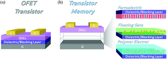
Transistor, as it stands for “trans resistor” or “transfer of resistor” device, is a unique electronic component that could precisely control the resistance/conductance across a semiconducting channel by finely tuning the strength of the electric field. Consequently, the device could regulate the current or voltage flow that acts as a switch or gain the electrical signals that are extremely useful to logic or analog circuitries, and many functional components.1–3 The device possesses three terminals that are the so-called source (S), drain (D), and gate (G). In addition, in between the source/drain and gate, its conventional architecture has to contain a semiconductor and dielectric/blocking layer, as described in Fig. 1a.As information technology has rapidly progressed, nowadays, many innovations in electronic components have also been developed specifically in response to the fields of the Internet of Things (IoT) and artificial intelligence (AI).4–6 For instance, a high-density data storage,7,8 a pulse monitoring sensor,9 an artificial synapse,10,11 a smart artificial retina,12 a photorecorder,13,14 pattern/image identification,15,16 and an ultrasensitive photodetector;17 all have been built-up based on a memory transistor framework. The clear difference between a memory transistor and a conventional one is in at least one additional polarization/charge storage layer that is sandwiched within the semiconductor and the gate contact (see Fig. 1b). This polarization/charge storage layer can extend the modulation of electrical behavior, thus establishing more pronounced hysteresis and/or threshold voltage shift (Vth) in the transfer characteristic of the transistor in order to incredibly improve memory performances.18–20 In general, the transistor memories could be classified into three different types based on their polarization/charge storage materials,21 as follows: (1) ferroelectric,18,19 (2) floating-gate,20,22–24 and (3) polymer electret transistor memory.7,11,13,14 Among them, the polymer electret one can behave as a semi-permanent electric field and/or dipole moment that is formed by trapping electrostatic charges.25,26 Besides this extraordinary function, the fabrication of transistor memory using polymer electrets is the most facile choice under solution processes and can be readily applied and adapted to many other processing methods from research scale to industrial applications.27–30 As a result, rapid progress in the polymer electret-based transistor memories has been revealed.
Nevertheless, all of those memory devices typically operate under continuous/pulses electrical gate bias to control the memory behavior.26 As such, it will cost more energy consumption, and more importantly, the transfer rate of the electrical signals will be limited to the speed of the charge transfer inside the circuitries.31 A breakthrough has been made by incorporating photoactive materials into a polymer matrix24 or in situ inheriting the photoactive properties of polymeric electrets via rational molecular design.13,14,32 Since the photo-modulated transistor memory could allow high-speed optical signal transfer and less noise, bundling with low energy operation, this has becomes a new major direction in the field.20 Such photoactive materials with optical physics properties (e.g., optical band gap, emission lifetime, exciton generation/annihilation)33 that benefit the transistor memories when the material interacts with light-matter (photon), establishing the novel transistor photomemory. The absorbed photons’ energy in photoactive materials will generate excitons (electron–hole pairs) that are directly involved in the charge trapping (charging electret) or recombination (neutralizing electret) process. Thus far, the device operations and its working principles have been discovered, such as photo-writing,14 photo-recovery,34 and else. Ultimately, the photonic transistor memory can be further operated partially34 or even fully10,35,36 by light to control the electrical properties of the device, which is in contrast to the electrically controlled alone.
Along with the countless variety of photoactive charge storage materials for transistor photomemories, the diverse structures, device operations, and physical mechanisms have been investigated and proposed, scrambling and piling up the abundance of new information in the field and producing the obscurity of its boundaries. Therefore, a clear classification of photonic transistor memories in terms of device operations and physical mechanisms that govern the memory behavior is required to serve as useful guidance. To the best of our knowledge, there have not been any reported cases in the field. In this review, we concisely elaborate the progress of photoactive materials used in organic transistor photomemories, as well as their device performances, and then systematically classify the physical device mechanisms in relation to their memory behavior and device operations. The present review will give hints for the design of organic transistor photomemories, and also offers to catalog each type that could assist the researchers in unfamiliar fields to clearly spot the differences of the device mechanisms, regardless of the photoactive charge storage layers employed in the device.
2. Basic operation of transistor memories and its important parameters
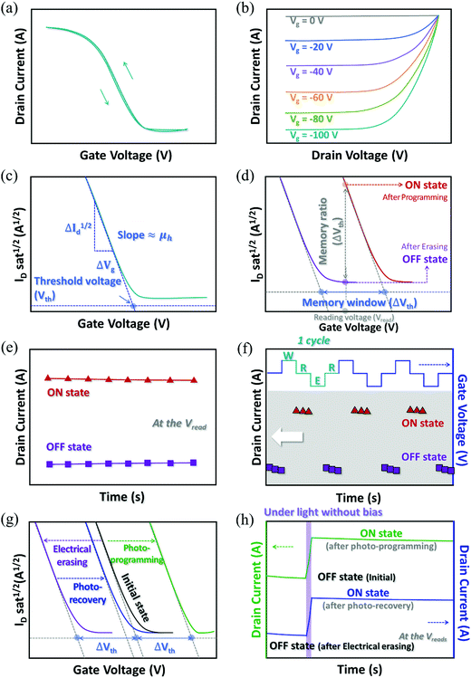
For the conventional transistor device (see Fig. 1a), assuming a p-type organic semiconducting (OSC) channel is employed, the application of an adequately high negative gate voltage (Vg) will induce the holes to accumulate at the bottom semiconductor interface and form the conductive accumulation region. At this stage, a negative voltage difference (Vds) between the drain and source electrodes can drive the hole current in the accumulation mode, resulting in the high output drain current (Id). This conventional transistor device is typically evaluated by measuring the transfer characteristic curve (Idvs. Vg) and output characteristic curve (Idvs. Vds) as demonstrated in Fig. 2a and b, respectively. Accordingly, one of the important parameters to evaluate the transistor performances, that is, field-effect charge carrier mobility (μ) can be deduced from the slope of Id1/2vs. Vg curve described in Fig. 2c.37,38 The interception of its linear curve to the Vg axis will give the threshold voltage (Vth) value of the device, which is defined as the minimum Vg bias to stimulate the output Id.On the other hand, for the transistor memory, several additional parameters such as Vth shift (ΔVth; memory window), memory ratio, retention time, endurance cycles and/or write-read-erase-read (WRER) cycles are essential to determine the performances of memory behavior.26 A large Vth shift is highly desirable, which leads to a broad memory window and memory ratio to properly distinguish the memory levels. The Vth shift on transistor memory can be realized by the application of Vg bias at a time period that is so-called electrical “programming” or “erasing” (see Fig. 2d) depends on how the device behaves to the negative or positive Vg bias. This programming or erasing process will result in changes in the Vth and output Id values when the device runs in the reading mode using the same fixed Vg and Vds. The memory ratio is then determined by the ratio between high (“on” state) and low (“off” state) output Id values. Not to mention that the output Id values, either in the on or off state, have to be stable i.e., the on or off state is utterly unchanged over time after programming or erasing treatment, reflecting the non-volatile memory type of the device. This capability can be evaluated through a retention time of at least 104 s (see Fig. 2e), and finally, as demonstrated in Fig. 2f, the WRER operations on the memory device can be also used to evaluate the stability and endurance of the dynamic changes in memory states.
Furthermore, in the photonic-based transistor memories, light exposure to the device at a time period (no bias on Vg and Vds, merely illuminated by light) can also alter the Vth value.33 Namely the process called, “photo-writing” or “photo-recovery” causes the Vth to shift away or come close to the initial state. Fig. 2g represents how the photo-writing or photo-recovery process shifts the Vth value of the device. Following the changes of Vth by light illumination, a simple evaluation to prove the authentication of photonic memory device is by monitoring the evolution of output Id during a light pulse to the device as portrayed in Fig. 2h. Interestingly, aside from exposure time, the light properties that illuminate the photonic memory device also strongly affect the memory behavior, for instance, different light wavelengths (photon energy) and light intensities/powers.39 Hence, this phenomenon ignites another important parameter named “photosensitivity”8 and “photoresponsivity”.36 Although, both photosensitivity and photoresponsivity are defined as the changing portion of output Id due to light irradiation, yet, the photoresponsivity may offer a better comparison study since the changes in output Id are normalized by the incident illumination power.
3. Effects of photoactive charge storage materials on the memory characteristics
To date, plentiful photoactive materials have been explored and incorporated into the fabrication of high-performance photonic transistor memory devices. In brief, in this section, we will discuss some photonic memories employing various photoresponsive charge storage materials such as inorganic perovskite/insulated polymer blending based floating gates,7,24,40–42 strong intramolecular donor–acceptor (D–A) and aggregation-induced-emission (AIE) conjugated polymer electrets,13,14,32 and supramolecular based polymer electrets.43–45 In the case of other photoactive charge storage material developments (such as rod-coil or rod-like liquid crystals, hybrid metal/metal-oxide nanoparticles/thin-films, metal–organic frameworks, photochromic blends/monolayers, biomass-derived electrets, and small-molecules based), and other unique morphologies/topologies of charge trapping interfaces, as well as device structures that are not covered in this section, could be found in the recently published reports and reviews.22,23,46–58 Below, the device structures and its memory characteristics to the device operations will be elaborated in detail.3.1. Blended perovskite/insulated polymer photoresponsive floating gates
Owing to the strong light-harvesting capability, low exciton binding energy, and long charge carrier lifetime (>100 ns) and diffusion length (>1 μm), inorganic perovskite-based materials have been chosen as versatile and promising photoresponsive materials.24,40,59–63 For photomemory applications, typically perovskite nanoparticles (NPs) will be mixed with polymer insulation to control the film morphology and suppress the formation of the continuous perovskite film that might favor a pass way for depleting the trapped charges.24,64 By this method, the formation of the charge storage layer could be regarded as the floating gate type. The first work on this idea was actually reported by Chen et al. in 2017.24 They blended MAPbBr3 perovskite NPs with a polystyrene (PS) polymer matrix as the photoresponsive floating gate. Fig. 3a represents the device structure and the scanning electron microscopy (SEM) and transmission electron microscopy (TEM) images of the MAPbBr3/PS composite film in the report. The SEM and TEM images clearly indicate the discrete formation and well-dispersed MAPbBr3 NPs in the PS matrix, which can effectively strengthen the charge trapping capability to realize the nonvolatile characteristics of the derived photomemory. As depicted in Fig. 3b, the manufactured device can exhibit a positive shift of Vth after the photo-writing process (UV light, 365 nm) for 120 s, implying that the perovskite blended PS floating gate can serve as the electron trapping sites. Fig. 3c demonstrates the memory retention time over three months after photo-writing, which further confirms the excellent charge storage stability. The neutralization of the photomemory device can be performed with electrical erasing by Vg of −60 V for 1 s, causing the transfer curve to shift back to the initial state. Following this study, Ercan et al. investigated the influence of different polymer matrices on the photoresponse and memory properties of perovskite-based photomemories.64 In the report, all perovskite-based devices showed the transfer curve shift to the positive region after photo-writing treatment with blue light (450 nm) for 120 s. However, only two devices with polystyrene (PS) and poly(4-vinylphenol) (PVPh) host polymer matrixes can revert the transfer curve to the initial state via an electrical erasing process (at Vg of −60 V). Additionally, Chang et al. have successfully fabricated a perovskite-based device with an exceptionally faster photo-writing time (ca. 5 ms) by introducing polystyrene-block-poly(ethylene oxide) (PS-b-PEO) as a polymer matrix shown in Fig. 3d.59 The transfer curves of the devices also showed displacement towards the positive region upon the photo-writing process by green light (520 nm), displayed in Fig. 3e and f. With an erasing voltage pulse of about −60 V for 1 s, the device can be returned to its initial state, as caused by the charge neutralization due to hole injection. In a recent report, by adding phenylethylammonium bromide (PEABr) in polystyrene-block-poly(ethylene oxide) (PS-b-PEO)/FAPbBr3 blends as the photoresponsive charge storage layer (see Fig. 3g), the degree of preferential orientation of perovskite crystallites towards the vertical axis can greatly enhance the charge transfer efficiency as well as the memory characteristics. It turned out that the same trend of transfer curve changes upon photo-writing (by blue light (450 nm), 240 s) and electrically erasing (at Vg of −60 V, 1 s) operations can be observed as illustrated in Fig. 3i and j.61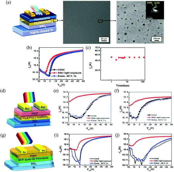 | ||
| Fig. 3 (a, d and g) Show the device structures of various photonic memory devices using perovskite based floating gates. (b and c), e, f, i and j) show their associated transfer curves after different photo-writing treatments and electrical erasing processes. (a–c) Reprinted with permission from ref. 24. Copyright 2017 WILEY-VCH Verlag GmbH & Co. KGaA, Weinheim.24 (d–f) Reprinted with permission from ref. 59. Copyright 2020 WILEY-VCH Verlag GmbH & Co. KGaA, Weinheim.59 (g–j) Reprinted with permission from ref. 61. Copyright 2022 Wiley-VCH GmbH.61 | ||
Unlike most transistor photomemories that partially rely on an electrical bias to perform a complete cycle of WRER, Liao et al. have conceptually developed a novel fully optically driven photomemory based on Cs2Pb(SCN)2Br2 perovskite and poly(vinylpyrrolidone) (PVP) polymer blends seen in Fig. 4a.35 The photo-writing and photo-recovery operations of the device can be attained by using two different light sources, i.e., white light and a blue laser, producing in-transfer curve shift further of and close to the initial state, respectively, as depicted in Fig. 4b and c. A fully light-controlled photomemory device (comprising n-type N,N′-bis(2-phenylethyl)perylene-3,4,9,10-bis(dicarboximide) (BPE-PTCDI) and hybrid floating gate of CH3NH3PbBr3/poly(2-vinylpyridine) (P2VP)) has also been reported by Yang et al. as displayed in Fig. 4d.36 They demonstrated in Fig. 4e–g, the full light control operations by using various visible lights (650, 530, and 405 nm) to enable photo-writing and a UV light (254 nm) in the photo-recovering process.
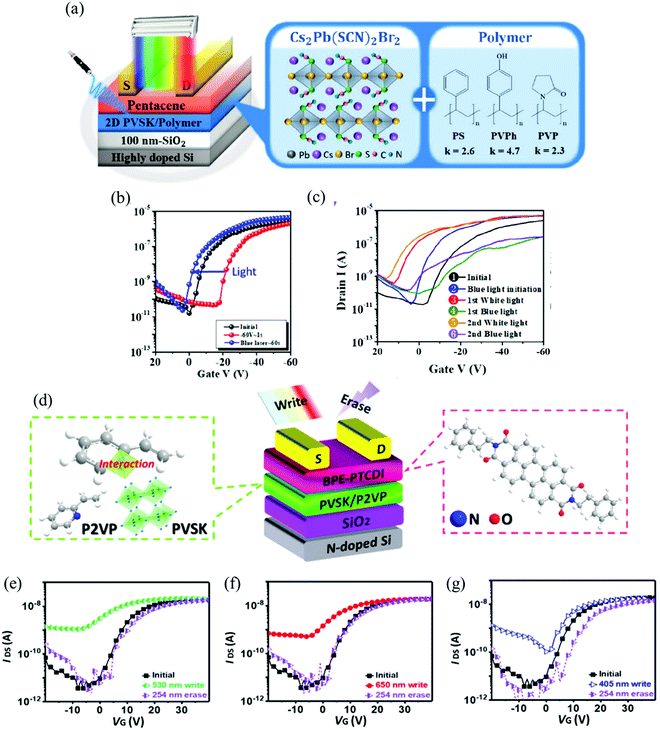 | ||
| Fig. 4 (a and d) show the device structures of fully optical driven photomemory based floating gates along with the chemical motifs and perovskite structures. (b, c, e, f and g) show the respective transfer curves after treatment with various light wavelengths for photo-writing and photo-recovery processes. (a–c) Reprinted with permission from ref. 35. Copyright 2020 American Chemical Society.35 (d–g) Reprinted with permission from ref. 36. Copyright 2021 American Chemical Society.36 | ||
Subsequently, we summarized the memory characteristics of several perovskite-based floating gate photomemory transistors as tabulated in Table 1, including their device operations and conditions for a clearer comparison.
| SiO2 thickness | Photoactive charge storage material | Programming/erasing operation (V) | Programming/erasing time (s) | ΔVth (V) | I ON/IOFF ratio | Retention time (s) | Ref. |
|---|---|---|---|---|---|---|---|
| * Abbreviations: PS, Polystyrene; PVPh, poly(4-vinylphenol); pero, CH3NH3PbBr3; BCP, block-copolymer; PCDTPT, poly[1,2,5]thiadiazolo[3,4-c]pyridine-4,7-diyl(4,4-dihexadecyl-4Hclopenta[2,1-b:3,4-b0]dithiophene-2,6-diyl)[1,2,5]thiadiazolo[3,4-c]pyridine-7,4-diyl(4,4-dihexadecyl-4H-cyclopenta[2,1-b:3,4-b0]dithiophene-2,6-diyl); OS, oligomeric silica; RP-17, poly(3-hexylthiophene-co-thiophene); βNC, β-cyclodextrin modified CH3NH3PbBr3; P3HT, poly(3-hexylthiophene-2,5-diyl);FA-QDs, FAxCs1−xPbBr3; PVP, poly(vinylpyrrolidone); P2VP, poly(2-vinylpyridine). | |||||||
| 100 | MAPbBr3/PS | Light (365 nm)/−60 | 120/1 | 6.7 | ∼104 | 104 | 24 |
| 100 | PVPh-pero | Light (450 nm)/−60 | 120/1 | ∼31.5 | ∼105 | >103 | 64 |
| 100 | BCP-1/MAPbBr3 | Light (520 nm)/−60 | 240/1 | — | ∼104 | 104 | 59 |
| 100 | PCDTPT/CsPbBr3 | Light (300 nm)/−10 | 0.5/0.1 | 66.5 | ∼104 | 104 | 41 |
| 100 | Cs2AgBiBr6@OS | Light (450 nm)/−40 | 60/0.1 | 58 | ∼104 | 104 | 42 |
| 100 | RP-17/βNC | Light (405 nm)/−60 | 120/1 | 18.34 | ∼103 | >104 | 40 |
| 300 | P3HT/FA-QDs | Light (520 nm)/−100 | 120/1 | — | ∼104 | — | 60 |
| 100 | BCP/FAPbBr3–5% PEABr | Light (450 nm)/−60 | 240/1 | — | ∼104 | 104 | 61 |
| 100 | MAPbBr3/P2VP | Light (530 nm)/light (254 nm) | 20/1 | — | ∼104 | 104 | 36 |
3.2. Photoactive conjugated D–A and AIE based polymer electrets
Compared to photoresponsive inorganic perovskite-based floating gates, photoactive D–A and AIE conjugated polymers provide simpler device manufacturing without additional polymer matrixes. The strong intramolecular interaction between electron-donating and electron-accepting moieties renders an exceptional charge separation ability to facilitate the dissociation of excitons into free charges.13,14,32,65,66 Hence, the extra photogenerated charges could boost photomemory characteristics upon the dynamic operations with light. Besides, through rationale design and careful selection of the donor and acceptor groups, the energy levels of the highest occupied molecular orbital (HOMO) and lowest unoccupied molecular orbital (LUMO) of the resulting molecules/polymers can be finely tuned to match the energy alignment to favor efficient charge transfer.67,68 Not only that, the changes of HOMO and LUMO levels could affect the photophysical properties, i.e., optical band gap,37,69 and benefitting the device operations with specific photon energy for less light interference.While using D–A framework polymers for the photosensitive charge storage layer, Chen et al. designed an electret called Poly CD that comprises carbazole moiety as a donor and a dioxazine moiety as an acceptor.13 Such attentive molecular design for the retention properties of memory devices has also been made by employing bisphenol A with a soft ether linkage instead of the fully conjugated structures that could dissipate the stored charges via a conductive route. Fig. 5a shows the chemical structure and device architecture in the report. The device embedded photoactive Poly CD can be electrically programmed to move the Vth away from the initial state and photorecovered that went vice versa, as shown in Fig. 5b and c. However, surprisingly, the Poly CD can also store both positive and negative charges, implying the ambipolar behavior of the charge storage electrets that could be applied to p-type or n-type semiconductor active channels. Aside from D–A conjugated polymer electrets that commonly show aggregation-caused quenching (ACQ) effect, the use of novel aggregation-induced emission (AIE) polymers as an electret layer could further switch the storage behavior of non-volatile memory from flash to write-once-read-many (WORM) by tailoring the torsion-angle between the motif of the donor and acceptor moieties (see Fig. 5d).14 This has been recently reported by Ke et al. that the AIE polymer electrets could perform the photo-writing operation (by blue light, 405 nm), impacting the transfer curve shift away from the initial state, as presented in Fig. 5e and f. They claimed that the first authentic ultrafast photoresponse time achieved 0.1 ms among the polymer-based transistor photomemories. Not only that, the device performed with a stunning current switch ratio of about 106 and retention time of over 40![[thin space (1/6-em)]](https://www.rsc.org/images/entities/char_2009.gif) 000 s, which is attributed to the instantaneous recombination of the forming interlayer excitons immediately after light stimulation to the AIE polymers at the interface within the active semiconductor and AIE polymer even in the absence of applied vertical and parallel electric fields.
000 s, which is attributed to the instantaneous recombination of the forming interlayer excitons immediately after light stimulation to the AIE polymers at the interface within the active semiconductor and AIE polymer even in the absence of applied vertical and parallel electric fields.
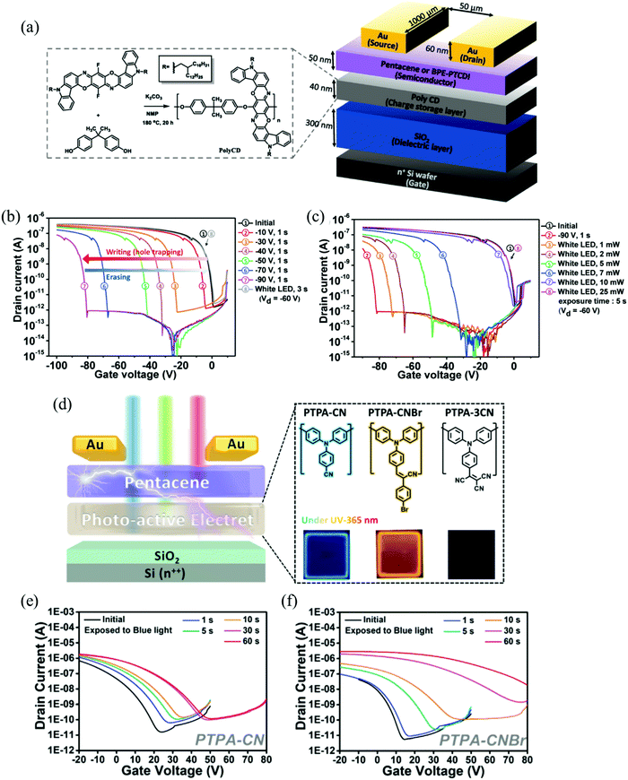 | ||
| Fig. 5 (a and d) show device structures of polymer electrets based photomemories, including the chemical motifs of donor–acceptor moieties. (b, c, e and f) show the respective transfer curves after a variety of electrical programming, photo-recovery, and photo-writing processes. (a–c) Reprinted with permission from ref. 13. Copyright 2019 WILEY-VCH Verlag GmbH & Co. KGaA, Weinheim.13 (d–f) Reprinted with permission from ref. 14. Copyright 2021 Wiley-VCH GmbH.14 | ||
Table 2 summarizes some photonic transistor memory performances using D–A and AIE conjugated based polymer electrets.
| SiO2 thickness | Photoactive charge storage material | Programming/erasing operation (V) | Programming/erasing time (s) | ΔVth (V) | I ON/IOFF ratio | Retention time (s) | Ref. |
|---|---|---|---|---|---|---|---|
| * Abbreviations: PolyCD, carbazoledioxazine polymer; copoly(CBT), carbazole/thiophenebenzothiadiazole–thiophene copolymer; PTPA-3CN, poly[4-(tricyanovinyl)phenyl]diphenylamine; PTPA-CNBr, [4-(α-cyanostilbene)phenyl]diphenylamine; PFO, poly(9,9-dioctylfluorene); POXD, poly (vinylphenyl oxadiazole). | |||||||
| 300 | PolyCD | −90/light (white LED) | 1/5 | 82 | ∼105 | 104 | 13 |
| 300 | Copoly(CBT) | −90/light (white LED) | 1/5 | 49 | ∼103 | 104 | 65 |
| 300 | PTPA-3CN | −100/light (365 nm) | 1/0.5 | 60 | ∼104 | 104 | 14,32 |
| 300 | PTPA-CNBr | −100/light (405 nm) | 1/0.1 | 18 | ∼106 | >104 | 14,32 |
| 100 | PFO-b-POXD10 | −60/light (254 nm) | 5/5 | 20.14 | ∼105 | >104 | 66 |
| 300 | PFO | −100/light (254/365 nm) | 5/1 | 78 | ∼107 | 104 | 34 |
3.3. Photoactive supramolecular based polymer electrets
Beyond the D–A and AIE conjugated polymers as elucidated previously, the novel supramolecular-based electrets also exhibit astounding charge transfer properties through non-covalent interactions70–72 between the self-assembly packing structure of the donor and acceptor moieties.73 Hence, the discrete configuration of supramolecular-based electrets can ensure better stability of the trapped charges within the respective host–guest molecules.In the early stages, the electrically operating supramolecular-based memory devices have been moderately inspected.74–76 However, just recently, the incorporation of photoactive supramolecular electret into the memory device has been reported and it showed superior bistable memory switchability with instantaneous photo-recovery capability under UV (365 nm) and green light (525 nm).43 In this report, Yang et al. have intensively investigated the photoactive supramolecular electret that constitutes of poly(1-pyrenemethyl methacrylate) (PPyMA) host polymer and 7,7,8,8-tetracyanoquinodimethane (TCNQ) guest molecule. Fig. 6a shows the host polymer and the guest molecule structure and the device layout of the supramolecular electret-based photonic memory transistor. The modulated transfer curves displayed in Fig. 6b–e behave distinctively with different contents of TCNQ molecules under Vg bias of −50 V for 1s (resulting in more negative Vth) and various photorecovery durations (resulting in the Vth shifts to the positive direction) with UV light. It showed that with an equivalent molar content of pyrene (as a functional moiety in the host polymer) and TCNQ (as a guest molecule), the associated device (PPyT-2) performed exquisitely along with a wide memory window (ΔVth = 34 V), large memory ratio of about 3.1 × 10⁶, long retention capability over 104 s, and robust memory endurance (WRER cycles over 100).
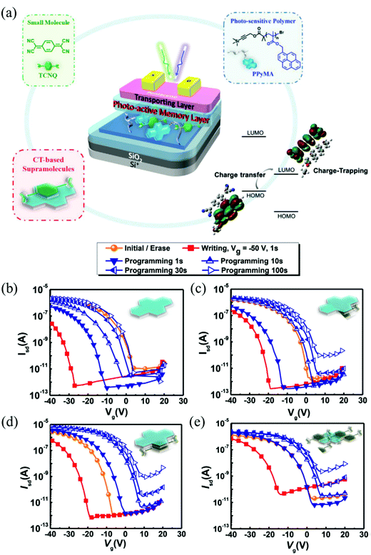 | ||
| Fig. 6 (a) The device structure and chemical motifs of the host polymer and guest molecules in supramolecular electret-based photomemory. (b–e) Transfer curves of the respective devices with various concentrations of guest molecules. Reprinted with permission from ref. 43. Copyright 2021 Wiley-VCH GmbH.43 | ||
To clarify the supramolecular-based transistor memory performances, both electrically controlled and partially photo-driven devices are recapitulated in Table 3.
| SiO2 thickness | Photoactive charge storage material | Programming/erasing operation (V) | Programming/erasing time (s) | ΔVth (V) | I ON/IOFF ratio | Retention time (s) | Ref. |
|---|---|---|---|---|---|---|---|
| * Abbreviations: P4VP, poly(4-vinylpyridine); AM4, 1-aminopyrene; PI, polyimide; PPyT-2, poly(1-pyrenemethyl methacrylate) + 50 mol% 7,7,8,8-tetracyanoquinodimethane (TCNQ). | |||||||
| 300 | P4VP(2-naphthol) | 100/−100 | 1/1 | 61 | >107 | 104 | 75 |
| 100 | AM4/PI | 40/−40 | 1/1 | 29.95 | >104 | 104 | 76 |
| 100 | PPyT-2 | −50/light (365 nm) | 1/100 | 34 | >106 | 104 | 43 |
4. Physical device mechanism in association with the device operations
In this section, the physical mechanism of photonic transistor memories will be elucidated in more detail according to the Vth shift response upon the device operations as observed in the previous section. Then, in general, as illustrated in Fig. 7, the working principles of photomemory transistors could be divided into several categories as follows: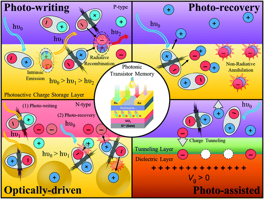 | ||
| Fig. 7 A representation of the device operations along with its process mechanisms that are applied in the photonic memory transistor devices. | ||
4.1. Photo-writing mechanism
Photo-writing phenomenon can be observed when the transfer curve shifts away from the initial state after the excitation of the photoresponsive charge storage layer with light exposure, resulting in high throughput Id in the reading mode. As was exemplified in the previous section, often, the perovskite-based floating gate photonic memory device unveils this phenomenon. Thus, to elucidate the plausible process mechanism for the photo-writing operation, we brought the arguments from Chen's report24 involving a simple system based on perovskite/insulating polymer blend floating gate photonic memory, as displayed in Fig. 3a. In general, the photophysical properties and frontier molecular orbital energy levels (HOMO and LUMO) of both, the active layer and photoactive material, are essential to be clarified, as the photoinduced generation of free charges, charge transfer behavior, charge polarities, as well as, charge trapping abilities will be strictly correlated to the memory behavior upon the device operations. Fig. 8a shows the absorption spectra of the MAPbBr3/PS composite film in comparison to the pentacene film. As can be expected, the MAPbBr3/PS composite film possesses distinct absorption regions against the pentacene film, which makes it less absorbing interference. Moreover, the PL spectra in Fig. 8b confirms the efficient photoexcitons’ dissociation and charge transfer in between the MAPbBr3/PS composite film on pentacene, which is demonstrated by a rapid PL quenching compared to the controlled MAPbBr3/PS composite film on quartz. Following this scheme, the corresponding schematic band diagrams of pentacene, perovskite MAPbBr3, and PS materials can be drawn, as shown in Fig. 8c to explain the process mechanism. Upon the photo-writing, the incident light source with photon energy closely matching the perovskite band gap energy will be absorbed properly and in turn generate more hot photoinduced carriers within the confined perovskite nanoparticles. Owing to the low conduction band of the perovskite material, the photoinduced electrons will remain and be stabilized in the perovskite, whilst the photogenerated holes will likely tunnel through the PS matrix and transfer to the HOMO level of pentacene. It is worth noting that the spatially discrete distribution of perovskite nanoparticles in the PS matrix can effectively suppress the charge trapping dissipation.24 Subsequently, this situation creates an internal built-in electric field that provides the hole accumulation region, furnishing the unchanged state of the photonic memory device. On the other hand, the charged device due to the trapped electrons in perovskite nanoparticles can be neutralized by applying the negative Vg bias that will draw the holes from the HOMO level of pentacene and overcome the potential barrier of the PS matrix and then recombine non-radiatively with the trapped electrons.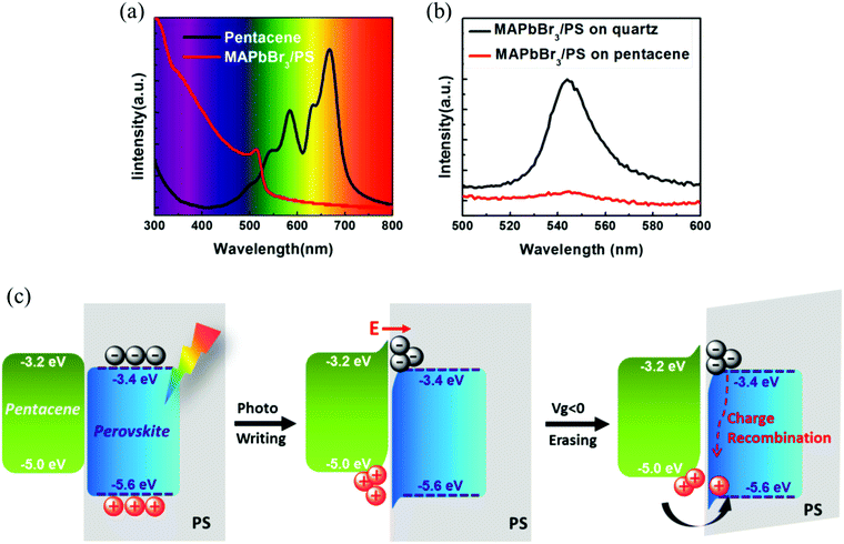 | ||
| Fig. 8 (a) Optical absorption spectra of the pentacene film and MAPbBr3/PS composite film. (b) PL characteristics of the MAPbBr3/PS composite film on quartz and on pentacene with light excitation at 450 nm. (c) Photo-writing and electrical erasing process mechanisms. Reprinted with permission from ref. 24. Copyright 2017 WILEY-VCH Verlag GmbH & Co. KGaA, Weinheim.24 | ||
There also occurred a photo-writing behavior of the photonic memory devices based on AIE polymer electret as mentioned earlier, as shown in Fig. 5d–f. Even though, it offers a simpler device preparation and less sophisticated system (solely a polymer electret in contrast to the floating gate system with two distinct materials), even so, the proposed plausible device mechanism is quite fascinating and implicates the interlayer excitons at semiconductor/AIE polymer electret interface.14Fig. 9a depicts the emission spectra of bilayer films of pentacene/AIE polymer electret (with an excitation wavelength of 405 nm) with the appearance of a new emission band of the interlayer excitons. It is elucidated from the schematic band diagrams portrayed in Fig. 9b. Owing to the difference in the HOMO levels for both AIE polymers and pentacene being higher than 0.15 eV, which is in the range of the binding energy of Frenkel excitons,77,78 the radiative relaxation pathway could be preferred. Hence, the noticeable new emission band in bilayer films could be attributed to the interlayer-recombined exciton from the LUMO level of pentacene and the HOMO level of AIE polymer.79–81 The photo-writing mechanism then could be elaborated, as illustrated in Fig. 9c. The photoactive AIE polymer-based electret layer firstly generates excitons upon exposure to blue light. Then, a fraction number of excitons established within the electret layer would self-recombine and hence emit its intrinsic emission spectrum. The emitted photons from the electret layer could effectively be absorbed by pentacene to produce its own excitons simultaneously, and eventually, each type of opposite photoinduced charge migrate to their suitable energy levels, where electrons reside in the electret layer and holes remain in pentacene. In this state, the transfer curve and Vth position of the device will shift away to the positive region, impacting the normally high output Id.
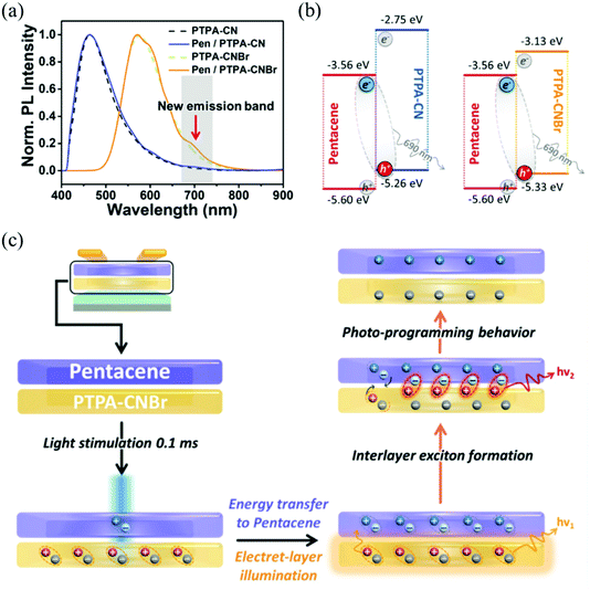 | ||
| Fig. 9 (a) Device structure of perovskite based floating photomemory, in line with the well-distributed perovskite nanoparticles within the polymer matrix. (b) Photo-writing and electrical erasing process mechanisms. Reprinted with permission from ref. 14. Copyright 2017 WILEY-VCH Verlag GmbH & Co. KGaA, Weinheim.14 | ||
4.2. Photo-recovery mechanism
Whereas the exact opposite of photo-writing, that is the photo-recovery phenomenon, the noticeable event occurs conversely. This implies that, the transfer curve of the device after receiving an appropriate light source by the photoactive charge storage layer, will lead to the displacement towards the initial condition. Indeed, the phenomenon will take place prior to the charging operation of the device (the transfer curve must be quite distant from the initial state after Vg bias programming). On numerous occasions, this phenomenon appears on the photonic memory devices employing photoactive polymer electrets, e.g., D–A and AIE conjugated polymers that have been presented in the previous section. Although some reports believe that the photo-recovery occurrence could be caused by the recombination of trapped charges with the photoexcitons from the semiconducting layer (i.e., pentacene),82 yet, other reports state that the photoactive electrets have a significant role in generating excitons that in situ instantaneously neutralizing the trapped charges within it.13,65 To confirm this aspect, Chen et al. reported such a straightforward demonstration.34 They directly engaged the photo-recovery operation between commercial photoactive polymer polyfluorene (PFO) electret and non-photoactive insulating poly(vinyl alcohol) (PVA) polymer under the same device configuration, as depicted in Fig. 10a. The aftermath showed that the device without photoinduced excitons’ ability (a device that employed PVA as an electret) was unable to exhibit a remarkable photo-recovery phenomenon. Although the light source exposed to the device can also excite the pentacene semiconductor layer, the study showed no conspicuous photo-recovery, as compared to PFO photonic transistor memory. Concisely, the photoresponsive polymer electret literally governs the in situ neutralization of the charged device. The photorecovery mechanism was then could be unveiled, as illustrated in Fig. 10c. In the beginning (see Fig. 10b), the device is electrically charged by exerting Vg at a negative bias to enable the hole trapping process in the polymer electret layer. Subsequently, a decent illumination of light on the photoactive polymer electret renders the photogeneration of electron–hole pairs that dissociate into electrons to in situ neutralize the trapped holes and the photoinduced holes that will be escaping to the HOMO level of pentacene. As a result, the eliminated trapped holes in the electret dispel the built-in electric field, yielding a neutral device with low output Id and/or recovering the device to its initial condition.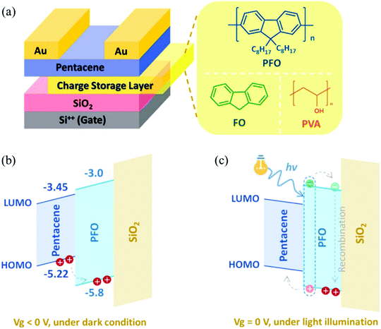 | ||
| Fig. 10 (a) Photomemory transistor structure with photoactive polymer electrets. (b) Electrical-programming and (c) photo-recovery mechanisms explained with schematic band diagrams. Reprinted with permission from ref. 34. Copyright 2021 American Chemical Society.34 | ||
4.3. Optically-driven mechanism
The fully optical controlled photonic memory transistor is an exceptional memory device. The device structure and memory behavior have been thoroughly described in the previous section shown in Fig. 4d–g. Such a device most likely has a photoactive charge storage layer containing two distinct photoactive materials that possess low band gap perovskite nanoparticles and a wide band gap P2VP polymer matrix (see Fig. 11a and b).36 Hence, the adoption of a floating gate type of charge storage layer into the device is the most suitable one for this application. On this account, the photoactive floating gate layer could be able to perform photo-writing and photo-recovery by using different photon energies (light wavelengths). As displayed in Fig. 11c and d, the device mechanism can be interpreted as follows: in the photo-writing step, first, the use of visible light (low photon energy; 405–650 nm) will produce photoexcitons in perovskite nanoparticles and/or BPE-PTCDI (depending on the absorption property of these two materials) and subsequently dissociated into photoinduced electrons and holes. Based on the favorable band energy matching illustrated in the schematic diagram, the electrons will migrate from the perovskite to BPE-PTCDI, whilst the holes are transferred oppositely. In this situation, the floating gate will preserve the holes that are possibly trapped at the perovskite/P2VP interface, and otherwise the electrons retained in BPE-PTCDI. The positively charged floating gate layer then induces a more electron accumulation region at the bottom interface of BPE-PTCDI, inflicting the high output Id of the device. On the contrary, the application of high photon energy (UV light; 254 nm) will perform the photo-recovery process on the device. Since the P2VP polymer matrix possesses a much wider band gap compared to perovskite and BPE-PTCDI materials, the UV light will be intensely absorbed and generate the photoexcitons, followed by excitons’ dissociation into free charge carriers. The photoinduced free charge carriers within P2VP eventually migrate to the adjacent perovskite nanoparticles and BPE-PTCDI, thus, neutralizing the respective trapped charges as well as the device.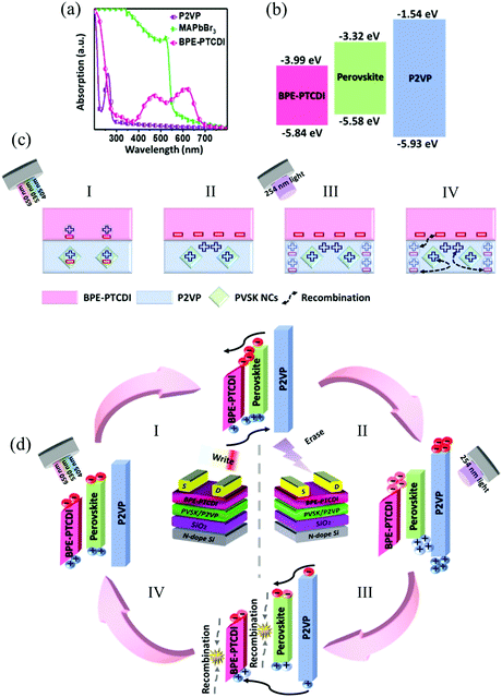 | ||
| Fig. 11 (a) Absorption spectra of n-type BPE-PTCDI, perovskite MAPbBr3, and polymer matrix P2VP. (b) The respective energy bands. (c) Charge migration upon photo-writing (charging electret) and photo-recovery (neutralizing electret) processes on the fully optical driven photonic memory transistor. (d) Schematic energy band diagrams in association with the photo-writing and photo-recovery processes. Reprinted with permission from ref. 36. Copyright 2021 American Chemical Society.36 | ||
4.4. Photo-assisted mechanism
From the device operation and mechanism, as listed above, it has been reported that the transistor memory devices could have an extra elevated memory performance when the light and Vg bias are exerted simultaneously. This operation, namely, “photo-assisted” programming or erasing has been intriguingly demonstrated in the literature.39,58,83–86 Several memory devices found in the literature that underwent these operations are tabulated in Table 4. However, what is more astonishing is that the regular transistor device without the photoactive material or charge storage layer could exhibit an outstanding memory characteristic. For the representative case, as shown in Fig. 12, a widely-used conventional OFET that constitutes a pentacene semiconducting channel on a silicon wafer with the octadecyltrimethoxysilane (OTS)-modified SiO2 layer can operate reversibly between the normal transistor and memory transistor devices flawlessly.8 Following this peculiar case, the authors highlighted that the photogenerated excitons and tunneling effect played a significant role in manifesting the photomemory behavior. In short, the photogenerated excitons stem from the semiconductor active channel upon illumination, whilst, the tunneling effect occurs at the same time when a sufficiently large electric field exists, driving the respective free charges (in the semiconducting channel) to overcome the tunneling barrier potential and get trapped (see Fig. 12). In the figure, photo-assisted programming (light exposure and a positive Vg bias) causes the separated free electrons to tunnel through a thin barrier of the OTS layer and fill up the intrinsic interface traps of the SiO2 layer. As a result, the trapped electrons would induce the hole accumulation region and transform the device with a normally high output Id. Henceforth, owing to the tunneling effect, when a large negative bias is applied during the erasing process, the majority of holes at the bottom interface of the pentacene layer can be drawn, overcoming the barrier potential, neutralizing the trapped electrons, and transforming the device into the neutral state. To this end, the concise and understandable mechanism with the above-mentioned straightforward results render the tunneling-effect in the photo-assisted transistor memory, as to be a new branch of research in this field that needs more attention. Besides, the concept is practically applicable to new photoactive semiconductors,33,44,87 novel photo-functionalized tunneling barrier materials,49,50,88 or even for the inherent rich surface traps of high-k dielectrics,89,90 which will provide more options for the improvement.| SiO2 thickness | Photoactive charge storage material | Programming/erasing operation (V) | Programming/erasing time (s) | ΔVth (V) | I ON/IOFF ratio | Retention time (s) | Ref. |
|---|---|---|---|---|---|---|---|
| * Abbreviations: PS, polystyrene; 6FDA-DBA-SP, poly(3,5-benzoic acid hexafluoroisopropylidene diphthalimide); PMMA, polymethylmethacrylate. | |||||||
| 200 nm | Au/PS nano-floating-gate | Light + 80/light + (−80) | 1 | 120 | ∼104 | 103 | 39 |
| 100 nm | 6FDA-DBA-SP | Light + 40/−40 | 10/1 | — | ∼104 | >104 | 84 |
| 300 nm | Au/Porous PMMA | Light + 80/−150 | 3 | 43 | ∼104 | 104 | 58 |
| — | Charge storage layer FREE | Light + 120/−120 | 10 | 59.7 | ∼106 | >104 | 85 |
| 300 nm | Ag/PMMA | Light + 10/light + (−10) | 1 | 1.67 | — | 105 | 86 |
| 300 nm | Charge storage layer FREE | Light + 100/−100 | 10 | 50.1 | ∼106 | 104 | 8 |
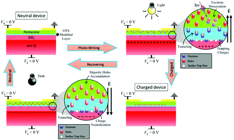 | ||
| Fig. 12 The mechanism process of photo-assisted programming and electrical erasing via tunnelling-effect of the photonic memory transistor device. Reprinted with permission from ref. 8. Copyright 2022 Wiley-VCH GmbH.8 | ||
5. Potential applications benefitted from transistor photomemory devices
As mentioned in the introduction section, many promising applications in the rapid growth of IoT4 and AI5,6 have been realized by adopting the concept of device operations and mechanisms of transistor photomemory.7–17 Among the plethora of applications, in this section, the discussion will focus on two crucial applications, there are multilevel storage memory cells7,8 and artificial synapses10,11 due to the similarity of working principle utilization;91 for other fascinating and feasible applications based on photonic memory devices can be found in the recent reports and literature reviews.20,30,44,50,92–975.1. Multilevel photomemory for high-density storage
The increased usage of data information in this era will likely burden the current storage technology, which keeps the data in a one-bit memory cell.98,99 Conventionally, increasing the density of memory cells to enlarge the storage capacity can be attained by scaling down a cell of memory devices. In doing so, albeit, this technique will soon face the difficulties owing to the physical and technical limitations. On the other hand, such a breakthrough concept to store multibit per cell of memory devices may solve the addressed issue and can be practically employed in the current technology.19,24,83,100–109 To achieve this purpose, a photonic memory device could generate distinguishable memory states in between the highest and lowest drain output current by precisely controlling the charge injection or the elimination rate under various device operations (gate bias strength, light intensity, and/or bias/exposure times) as discussed previously. In this regard, the number of trapped charges within the trapping sites will be responsible for the varied built-in potentials as well as the magnitude of the drain output current in a non-volatile way.For example, besides low power consumption and fast photomemory modulation, an article has reported an unprecedented photonic memory cell that could possess over 256 (8-bit storage) distinct current levels.100 The strategy was devised using the active channel blend of a common high-performance polymer semiconductor poly(3-hexylthiophene) and a photochromic diarylethene which can be switched under UV (closed isomer; appropriate energy levels for charge transfer) and green (opened isomer; inappropriate energy levels) light irradiation to control the rate of charge injection. The resulted memory device showed highly robust over 70 write-erase cycles, including the retained memory state over 500 days. In the recent report, the monitoring device for deep ultraviolet (DUV) light-sensing based on non-volatile photoelectric memory of OFET has demonstrated 16 distinct optical memory states (4-bit storage) and rewriting capability, indicating the superior multilevel memory behavior.110 Consisting of diketopyrrolopyrrole-dithienylthieno[3,2-b]thiophene (DPP-DTT) as an active channel, and poly(perfluoroalkenylvinyl ether) (CYTOP) on SiO2 substrate built-up the DUV photoelectric memory device along with retention of over 104 s, and more than 100 cycles of WRER operations. In the following progress, a transistor photomemory incorporating a ferroelectric (insulating) layer of poly(vinylidene fluoride-trifluoroethylene) (PVDF-TrFE) could offer several advantages compared to the conventional organic insulators111 by virtue of its relatively large fatigue-free remnant polarization,112 faster switching time, and better thermal stability.19,113,114 The yielded memory device is capable of operating in 11-bit storage per memory cell along with precise control of readout drain current and feasible repeatability, and even instant (milliseconds) and low light intensity (<1 μJ cm−2 s−1) of optical writing process.19
5.2. Photosynaptic transistor for visual perception
Meanwhile, the working principles, device operations, and capabilities of transistor photomemory have also been utilized in mimicking and emulating the complex biological functions such as nerve signal transmission to neuromorphic computing applications, and even recreating image memory for new-generation visual prosthetics and artificial visual perception systems such as a human eye (for example see in Fig. 13a).91,115–126 The so-called “photosynaptic transistor” resembles that of a biological synapse construction wherein the source/drain terminals can be associated with the pre-/postsynapses, and the external light stimuli/gate bias corresponds to the action potentials exerted in the presynapse (see Fig. 13b). The neurotransmitters within a synapse system could be represented as the charge carriers dwelling in the semiconducting layer within the source/drain circumference. In regard to this, the device mechanisms are quite similar, frankly speaking, the same to the mentioned physical working principles in the fourth section. Taken as an example from Fig. 13c, the respective band energies are drawn schematically based on the mixed quantum dot photoabsorbers and metal-oxide semiconducting layer that built-up a photosynaptic transistor in a recent report.115 Upon the incident light signal pulse to the device (an action potential exerted presynapse), the photogenerated electron–hole pairs in quantum dots (photoactive materials, in general) are readily separated, and subsequently, the electrons transfer to the most favorable energy level which is in the metal-oxide part. On the other hand, the holes are effectively confined in quantum dots because of an unfavorably high potential barrier.115 This mechanism is kind of similar to the photo-writing phenomenon for a transistor photomemory elaborated in the fourth section.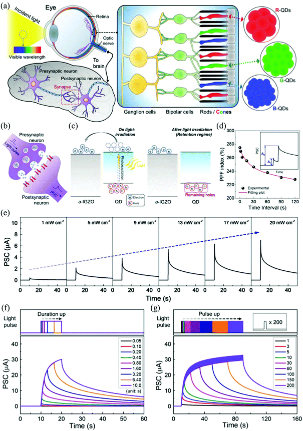 | ||
| Fig. 13 (a) An illustration of the human visual system in the human brain containing neurons and synapses. (b) An analogy of the biological synapse process. (c) Process mechanism in the energy band diagram. Photosynaptic behavior under light pulse stimuli: (d) pulse interval-dependent PPF index triggered by two spikes, (e) pulse intensity-dependent postsynaptic current (PSC), (f) pulse duration-dependent PSC, (g) pulse number-dependent PSC. Reprinted with permission from ref. 115. Copyright 2022 Wiley-VCH GmbH.115 | ||
Moreover, there are several key factors to be considered the synaptic behavior in photosynaptic devices, as follows: the excitatory postsynaptic current (EPSC) or inhibitory postsynaptic current (IPSC), which indicates an escalation (carrier capture) or depletion (carrier release) of the readout current in gauging the neuron connection (synaptic strength or weight); short-term plasticity/memory (STP/STM) and long-term plasticity/memory (LTP/LTM), indicate the flexibility to adjust the learning and recollection memory processes similar to the human brain. The STM characteristic itself could be indicated under the application of paired-pulse facilitation (PPF) or paired-pulse depression (PPD), which results in an increase or decrease in the ratio of postsynaptic current amplitude within the two successive spikes (see Fig. 13d). Whereas, the LTM relates to the slow decay of EPSCs as the synaptic weight increases with pulse width, the number of pulses, and its interval in attaining the spike number-dependent plasticity (SNDP), spike-time-dependent plasticity (STDP), and spike rate-dependent plasticity (SRDP). The entire factors above, in common, can be modulated by gate/drain bias or light intensity, wavelength, and exposure time in pulsing mode with different amplitudes/widths/frequencies/numbers to emulate both STM and LTM in the human brain, as exemplified in Fig. 13e to g. And most importantly, the energy consumption of photosynaptic transistor could be a great consideration,127 on account of emulating ultralow energy consumption per synaptic event (ca. 1–100 fJ) in the human brain.125,128,129 The energy consumption (Eon) can be estimated as Eon = Ipeak × t × V, where Ipeak, t, and V are the maximum peak value of the EPSC or IPSC, pulse duration time, and applied pulse voltage, respectively.60 Knowing these parameters for the photosynaptic transistor-based device is essential. In the latter paragraph, the progress of photosynaptic transistors will be elaborated on the latest reports found in the literature which are not limited to the use of photoactive organics/polymers,97,130,131 but also hybrid-inorganics and other potential photoactive materials.115,118,119,121,132
In our recent work on photosynaptic transistors, the use of single-walled carbon nanotubes (SWCNTs) wrapped single-layered poly(9,9-dioctylfluorene)-b-polyisoprene (PF-b-PI) which serves as both semiconductor and electret layer has demonstrated.11 Owing to the high charge carrier mobility of SWCNTs (∼11.3 cm2 V−1 s−1) and inherently photoactive conjugated polymer of PF-b-PI, this hybrid material endows the device with high output current (10−4 to 10−3 A) and finely-modulated synaptic behavior against either light or electrical signal. Besides possessing a large memory window (>70 V), the LTP to LTD could be emulated under 21 light pulses of blue light (395–415 nm at 25 mW cm−2) for 10 s each at the intervals of 30 s and continually monitoring the PSC in the dark for 1000 s, and the synaptic PPF behavior by the application of pair of presynaptic light pulses for 10 s each at intervals of 300 s. The electrical triggered synaptic properties resulted in the PPF index (a time interval of the synaptic device, which follows a biexponential function to identify and decode information)20 that matches well with the biological counterpart. In addition to that, the higher EPSC triggered by the second spike is usually ascribed to the charges accumulated from the earlier spike that is not able to fully dissipate, inflicting the more trapped charges for the incoming spike.133 As for the perovskite-based photosynaptic transistors, the reported devices could consume ultralow energy per synaptic event (0.03–0.18 fJ)60,132 as close as in the human brain. Those were rationally and carefully designed, such as by investigating the influence of A-site substitution60 and the solution processing and pretreatment with ultrasonication and UV irradiation.132 On top of that, by introducing an ultra-thin charge carrier regulator layer that is hexagonal boron nitride (h-BN) sandwiched between perovskite quantum dots and graphene, such a device can impart improved the PPF index (up to ∼196%) which is required in realizing high-precision artificial visual perception system.121 Last but not least, the development of polymer-based photosynaptic transistors keeps pace with other potential materials.122,130,131,134 In this scope, a photosynaptic transistor utilizing P3HT-b-P2VP block copolymer active layer could emulate PPF, STDP/SRDP, and STP/LTP behaviors.130 The corresponding LTM can keep the current contrast to 105, the STM with a high PPF ratio of 1.38, and an ultralow energy consumption calculated ca. 0.56 fJ at an application voltage of –0.0003 V stimulated under blue light (450 nm, 2.2 mW cm−2, for 0.2 s). A simpler polymer-based photosynaptic device with capabilities to simulate various synapse-like behaviors such as EPSC, PPF, STM/LTM and its transition using DUV light was demonstrated.131 The device contains of P3HT as active channel and CYTOP as a modifying layer for the dielectric surface with ΔEPSC values recorded up to 6.2 nA under the exertion of a single light pulse intensity of 0.15 mW cm−2 and duration of 4 s. And the very recent progress on photosynaptic device that using the same concept of photo-assisted operations (see in subsection of 4.4), while investigating the effect of molecular weight (Mw) of polymer electret to the photosynaptic behavior have been reported.134 With poly(N-vinylcarbazole) (PVK) as the case study, such device could exhibit a larger memory window (28.2 V) bundling with an instantaneous programming speed of 1 ms for lower Mw PVK electret. The photosynaptic behaviors such as EPSC/IPSC, PPF/PPD, excellent tunability between STP and LTP, including high accuracy and STP-based RGB color recognition ability that could be further emulated on lower Mw PVK device by photo-assisted operations.
6. Summary and perspectives
To conclude, we have systematically presented the transistor memory device structures, basic device operations, and several important parameters used to take the measure the good performance of the memory devices. Furthermore, the novel photonic memory transistors equipped with various proposed new photoactive materials in the charge storage layer could have more versatile potential applications and facile manufacturing methods to fit in with current technological advancements. On top of that, the photomemory behavior could be delicately tuned in response to the device operations and working principles such as photo-writing, photo-recovery, and fully optically driven, depending on the rational design and material selection of the photoactive charge storage layer. All of which, benefitting from the photogenerated excitons of photoresponsive materials, the photonic memory transistor devices could offer more control on memory behavior, including low noise interference, high information security and energy consumption, and high-speed information transfer compared to ordinary fully electrically-controlled one.In addition, the new concept of photo-assisted programming and erasing, principally shows the distinction in device operations and working mechanisms to the mentioned photonic memory transistors. Taking the advantages from intrinsic interface traps of the dielectric layer as well as the tunneling layer to stabilize charge trapping, the switchable conventional to photomemory transistor could be a general strategy for creating multifunctional photonic memory devices. Besides, the method operations have successfully demonstrated in the charge storage layer free transistors to behave as a photomemory device, hence, guaranteeing a cost-effective and facile device fabrication, for more practical and high-performance device applications.
Author contributions
Y.-C. C. contributed to supervision. S. P. P. contributed to writing – the original draft. S. P. P. and Y.-C. C. were further contributed to conceptualization and writing – review and editing. M.-N. C. was contributed to visualization.Conflicts of interest
There are no conflicts of interest to declare.Acknowledgements
The authors thankfully acknowledge the financial supports from the Ministry of Science and Technology in Taiwan (MOST 109-2622-E-011-030, and MOST 110-2221-E-011-009).References
- K. K. N. Simon and M. Sze, Physics of Semiconductor Devices, John Wiley & Sons, 3 edn, 2006 Search PubMed.
- J. S. Park, W.-J. Maeng, H.-S. Kim and J.-S. Park, Thin Solid Films, 2012, 520, 1679–1693 CrossRef CAS.
- Y. Guo, G. Yu and Y. Liu, Adv. Mater., 2010, 22, 4427–4447 CrossRef CAS PubMed.
- W. Shi, Y. Guo and Y. Liu, Adv. Mater., 2020, 32, 1901493 CrossRef CAS PubMed.
- C. Wan, P. Cai, M. Wang, Y. Qian, W. Huang and X. Chen, Adv. Mater., 2020, 32, 1902434 CrossRef CAS PubMed.
- Y. Zang, F. Zhang, C.-A. Di and D. Zhu, Mater. Horiz., 2015, 2, 140–156 RSC.
- C.-C. Shih, Y.-C. Chiang, H.-C. Hsieh, Y.-C. Lin and W.-C. Chen, ACS Appl. Mater. Interfaces, 2019, 11, 42429–42437 CrossRef CAS PubMed.
- Z.-Y. Wei, S. P. Prakoso, Y.-T. Li and Y.-C. Chiu, Adv. Electron. Mater., 2022, 2101349 CrossRef.
- Z. He, J. Han, X. Du, L. Cao, J. Wang, C. Zheng, H. Lin and S. Tao, Adv. Funct. Mater., 2021, 31, 2103988 CrossRef CAS.
- T. Ahmed, M. Tahir, M. X. Low, Y. Ren, S. A. Tawfik, E. L. H. Mayes, S. Kuriakose, S. Nawaz, M. J. S. Spencer, H. Chen, M. Bhaskaran, S. Sriram and S. Walia, Adv. Mater., 2021, 33, 2004207 CrossRef CAS PubMed.
- M. M. Mburu, K.-T. Lu, N. L. Prine, A.-N. Au-Duong, W.-H. Chiang, X. Gu and Y.-C. Chiu, Adv. Mater. Technol., 2022, 2101506 CrossRef.
- C.-C. Hung, Y.-C. Chiang, Y.-C. Lin, Y.-C. Chiu and W.-C. Chen, Adv. Sci., 2021, 8, 2100742 CrossRef CAS PubMed.
- C.-H. Chen, Y. Wang, H. Tatsumi, T. Michinobu, S.-W. Chang, Y.-C. Chiu and G.-S. Liou, Adv. Funct. Mater., 2019, 29, 1902991 CrossRef.
- C.-Y. Ke, M.-N. Chen, M.-H. Chen, Y.-T. Li, Y.-C. Chiu and G.-S. Liou, Adv. Funct. Mater., 2021, 31, 2101288 CrossRef CAS.
- T. Xu, S. Guo, W. Qi, S. Li, M. Xu and W. Wang, ACS Appl. Mater. Interfaces, 2020, 12, 21952–21960 CrossRef CAS PubMed.
- Q.-B. Zhu, B. Li, D.-D. Yang, C. Liu, S. Feng, M.-L. Chen, Y. Sun, Y.-N. Tian, X. Su, X.-M. Wang, S. Qiu, Q.-W. Li, X.-M. Li, H.-B. Zeng, H.-M. Cheng and D.-M. Sun, Nat. Commun., 2021, 12, 1798 CrossRef CAS PubMed.
- Z. Shao, T. Jiang, X. Zhang, X. Zhang, X. Wu, F. Xia, S. Xiong, S.-T. Lee and J. Jie, Nat. Commun., 2019, 10, 1294 CrossRef PubMed.
- Z.-D. Luo, M.-M. Yang, Y. Liu and M. Alexe, Adv. Mater., 2021, 33, 2005620 CrossRef CAS PubMed.
- M. Carroli, A. G. Dixon, M. Herder, E. Pavlica, S. Hecht, G. Bratina, E. Orgiu and P. Samorì, Adv. Mater., 2021, 33, 2007965 CrossRef CAS PubMed.
- Y.-C. Lin, W.-C. Yang, Y.-C. Chiang and W.-C. Chen, Small Sci., 2022, 2100109 CrossRef.
- Y.-H. Chou, H.-C. Chang, C.-L. Liu and W.-C. Chen, Polym. Chem., 2015, 6, 341–352 RSC.
- Y.-C. Chiang, C.-C. Hung, Y.-C. Lin, Y.-C. Chiu, T. Isono, T. Satoh and W.-C. Chen, Adv. Mater., 2020, 32, 2002638 CrossRef CAS PubMed.
- H. Chen, Y. Zhou and S.-T. Han, Nano Sel., 2021, 2, 1245–1265 CrossRef CAS.
- J.-Y. Chen, Y.-C. Chiu, Y.-T. Li, C.-C. Chueh and W.-C. Chen, Adv. Mater., 2017, 29, 1702217 CrossRef PubMed.
- J.-S. Lee, J. Mater. Chem., 2011, 21, 14097–14112 RSC.
- P. Heremans, G. H. Gelinck, R. Müller, K.-J. Baeg, D.-Y. Kim and Y.-Y. Noh, Chem. Mater., 2011, 23, 341–358 CrossRef CAS.
- Q. Wang, Y. Xie, F. Soltani-Kordshuli and M. Eslamian, Renewable Sustainable Energy Rev., 2016, 56, 347–361 CrossRef CAS.
- Y. Jiang, J. Chen, Y. Sun, Q. Li, Z. Cai, J. Li, Y. Guo, W. Hu and Y. Liu, Adv. Mater., 2019, 31, 1805761 CrossRef PubMed.
- X. Guo, Y. Xu, S. Ogier, T. N. Ng, M. Caironi, A. Perinot, L. Li, J. Zhao, W. Tang, R. A. Sporea, A. Nejim, J. Carrabina, P. Cain and F. Yan, IEEE Trans. Electron Devices, 2017, 64, 1906–1921 CAS.
- A. Tavasli, B. Gurunlu, D. Gunturkun, R. Isci and S. Faraji, Electronics, 2022, 11, 316 CrossRef CAS.
- A. K. Tripathi, K. Myny, B. Hou, K. Wezenberg and G. H. Gelinck, IEEE Trans. Electron Devices, 2015, 62, 4063–4068 CAS.
- C.-Y. Ke, M.-N. Chen, Y.-C. Chiu and G.-S. Liou, Adv. Electron. Mater., 2021, 7, 2001076 CrossRef CAS.
- Y. Wakayama, R. Hayakawa and H.-S. Seo, Sci. Technol. Adv. Mater., 2014, 15, 024202 CrossRef CAS PubMed.
- M.-N. Chen, S.-W. Chang, S. P. Prakoso, Y.-T. Li, K.-L. Chen and Y.-C. Chiu, ACS Appl. Mater. Interfaces, 2021, 13, 44656–44662 CrossRef CAS PubMed.
- M.-Y. Liao, Y.-C. Chiang, C.-H. Chen, W.-C. Chen and C.-C. Chueh, ACS Appl. Mater. Interfaces, 2020, 12, 36398–36408 CrossRef CAS PubMed.
- W.-C. Yang, Y.-C. Lin, M.-Y. Liao, L.-C. Hsu, J.-Y. Lam, T.-H. Chuang, G.-S. Li, Y.-F. Yang, C.-C. Chueh and W.-C. Chen, ACS Appl. Mater. Interfaces, 2021, 13, 20417–20426 CrossRef CAS PubMed.
- S. P. Prakoso, S. Kumar, S.-L. Wu, G.-T. Ciou, Y.-J. Ke, S. Venkateswarlu, Y.-T. Tao and C.-L. Wang, ACS Appl. Mater. Interfaces, 2020, 12, 1169–1178 CrossRef CAS PubMed.
- S. P. Prakoso, Y.-J. Ke, D.-C. Huang, C.-L. Wang and Y.-T. Tao, J. Chin. Chem. Soc., 2022, 69, 440–449 CrossRef CAS.
- X. Gao, C.-H. Liu, X.-J. She, Q.-L. Li, J. Liu and S.-D. Wang, Org. Electron., 2014, 15, 2486–2491 CrossRef CAS.
- E. Ercan, Y.-C. Lin, L.-C. Hsu, C.-K. Chen and W.-C. Chen, Adv. Mater. Technol., 2021, 6, 2100080 CrossRef CAS.
- H. Yang, Y. Yan, X. Wu, Y. Liu, Q. Chen, G. Zhang, S. Chen, H. Chen and T. Guo, J. Mater. Chem. C, 2020, 8, 2861–2869 RSC.
- W. Lin, G. Chen, E. Li, L. He, W. Yu, G. Peng, H. Chen and T. Guo, ACS Appl. Mater. Interfaces, 2020, 12, 43967–43975 CrossRef CAS PubMed.
- Y.-F. Yang, Y.-C. Chiang, Y.-C. Lin, G.-S. Li, C.-C. Hung and W.-C. Chen, Adv. Funct. Mater., 2021, 31, 2102174 CrossRef CAS.
- H. Chen and J. Fraser Stoddart, Nat. Rev. Mater., 2021, 6, 804–828 CrossRef CAS.
- Y. Wang, D. Iglesias, S. M. Gali, D. Beljonne and P. Samorì, ACS Nano, 2021, 15, 13732–13741 CrossRef CAS PubMed.
- Y.-C. Lin, G.-S. Li, P.-J. Yu, E. Ercan and W.-C. Chen, J. Chin. Chem. Soc., 2022 DOI:10.1002/jccs.202200061.
- Y. Yang, Z. Li, C. Wu, W. Li, J. Wang, M. Yi and W. Huang, J. Mater. Chem. C, 2022, 10, 3292–3299 RSC.
- N. Shi, J. Zhang, Z. Ding, H. Jiang, Y. Yan, D. Gu, W. Li, M. Yi, F. Huang, S. Chen, L. Xie, Y. Ren, Y. Li and W. Huang, Adv. Funct. Mater., 2022, 32, 2110784 CrossRef CAS.
- S.-H. Yuan, D.-C. Huang and Y.-T. Tao, ACS Appl. Mater. Interfaces, 2022, 14, 7102–7108 CrossRef CAS PubMed.
- C. Xu, J. Zhang, W. Xu and H. Tian, Mater. Chem. Front., 2021, 5, 1060–1075 RSC.
- A.-C. Chang, Y.-C. Lin, H.-C. Yen, W.-C. Yang, Y.-F. Yang and W.-C. Chen, ACS Appl. Electron. Mater., 2022, 4, 1266–1276 CrossRef CAS.
- C.-K. Chen, Y.-C. Lin, J.-C. Ho, W.-C. Yang and W.-C. Chen, ACS Sustainable Chem. Eng., 2022, 10, 5268–5277 CrossRef CAS.
- K. Liang, R. Wang, B. Huo, H. Ren, D. Li, Y. Wang, Y. Tang, Y. Chen, C. Song, F. Li, B. Ji, H. Wang and B. Zhu, ACS Nano, 2022 DOI:10.1021/acsnano.2c00439.
- L. Zhou, S.-T. Han, S. Shu, J. Zhuang, Y. Yan, Q.-J. Sun, Y. Zhou and V. A. L. Roy, ACS Appl. Mater. Interfaces, 2017, 9, 34101–34110 CrossRef CAS PubMed.
- Y. Yu, Q. Ma, H. Ling, W. Li, R. Ju, L. Bian, N. Shi, Y. Qian, M. Yi, L. Xie and W. Huang, Adv. Funct. Mater., 2019, 29, 1904602 CrossRef CAS.
- Y. Wang, L. Kang, Z. Liu, Z. Wan, J. Yin, X. Gao, Y. Xia and Z. Liu, ACS Appl. Mater. Interfaces, 2021, 13, 13452–13458 CrossRef CAS PubMed.
- Q. Li, T. Li, Y. Zhang, Z. Chen, Y. Li, L. Jin, H. Zhao, J. Li and J. Yao, J. Phys. Chem. C, 2020, 124, 23343–23351 CrossRef CAS.
- M. Yi, J. Shu, Y. Wang, H. Ling, C. Song, W. Li, L. Xie and W. Huang, Org. Electron., 2016, 33, 95–101 CrossRef CAS.
- Y.-H. Chang, C.-W. Ku, Y.-H. Zhang, H.-C. Wang and J.-Y. Chen, Adv. Funct. Mater., 2020, 30, 2000764 CrossRef CAS.
- J.-Y. Chen, D.-L. Yang, F.-C. Jhuang, Y.-H. Fang, J.-S. Benas, F.-C. Liang and C.-C. Kuo, Adv. Funct. Mater., 2021, 31, 2105911 CrossRef CAS.
- Y.-H. Chao, J.-C. Chen, D.-L. Yang, Y.-J. Tseng, C.-H. Hsu and J.-Y. Chen, Adv. Funct. Mater., 2022, 2112521 CrossRef CAS.
- C.-H. Lin, L. Hu, X. Guan, J. Kim, C.-Y. Huang, J.-K. Huang, S. Singh and T. Wu, Adv. Mater., 2022, 2108616 CrossRef CAS PubMed.
- J. Pei, X. Wu, W.-J. Liu, D. W. Zhang and S.-J. Ding, ACS Nano, 2022, 16, 2442–2451 CrossRef CAS PubMed.
- E. Ercan, J.-Y. Chen, C.-C. Shih, C.-C. Chueh and W.-C. Chen, Nanoscale, 2018, 10, 18869–18877 RSC.
- C.-H. Chen, Y. Wang, T. Michinobu, S.-W. Chang, Y.-C. Chiu, C.-Y. Ke and G.-S. Liou, ACS Appl. Mater. Interfaces, 2020, 12, 6144–6150 CrossRef CAS PubMed.
- E. Ercan, Y.-C. Lin, C.-K. Chen, Y.-K. Fang, W.-C. Yang, Y.-F. Yang and W.-C. Chen, J. Polym. Sci., 2022, 60, 525–537 CrossRef CAS.
- S. A. Jenekhe, L. Lu and M. M. Alam, Macromolecules, 2001, 34, 7315–7324 CrossRef CAS.
- E. Busby, J. Xia, Q. Wu, J. Z. Low, R. Song, J. R. Miller, X. Y. Zhu, L. M. Campos and M. Y. Sfeir, Nat. Mater., 2015, 14, 426–433 CrossRef CAS PubMed.
- S. P. Prakoso, S.-S. Sun, R. Saleh, Y.-T. Tao and C.-L. Wang, ACS Appl. Mater. Interfaces, 2021, 13, 38365–38374 CrossRef CAS PubMed.
- S. De Feyter and F. C. De Schryver, Chem. Soc. Rev., 2003, 32, 139–150 RSC.
- A. Ajayaghosh, C. Vijayakumar, V. K. Praveen, S. S. Babu and R. Varghese, J. Am. Chem. Soc., 2006, 128, 7174–7175 CrossRef CAS PubMed.
- S. Guo, Y. Song, Y. He, X.-Y. Hu and L. Wang, Angew. Chem., Int. Ed., 2018, 57, 3163–3167 CrossRef CAS PubMed.
- A.-N. Au-Duong, C.-C. Kuo and Y.-C. Chiu, Polym. J., 2018, 50, 649–658 CrossRef CAS.
- H.-Y. Chi, H.-W. Hsu, S.-H. Tung and C.-L. Liu, ACS Appl. Mater. Interfaces, 2015, 7, 5663–5673 CrossRef CAS PubMed.
- Y. H. Chou, Y. C. Chiu, W. Y. Lee and W. C. Chen, Chem. Commun., 2015, 51, 2562–2564 RSC.
- W.-Y. Tung, M.-H. Li, H.-C. Wu, H.-Y. Liu, Y.-T. Hsieh and W.-C. Chen, Chem. – Asian J., 2016, 11, 1631–1640 CrossRef CAS PubMed.
- P. Cudazzo, M. Gatti and A. Rubio, Phys. Rev. B: Condens. Matter Mater. Phys., 2012, 86, 195307 CrossRef.
- J. Lee, S. S. Kim, K. Kim, J. H. Kim and S. Im, Appl. Phys. Lett., 2004, 84, 1701–1703 CrossRef CAS.
- H. Chen, X. Wen, J. Zhang, T. Wu, Y. Gong, X. Zhang, J. Yuan, C. Yi, J. Lou, P. M. Ajayan, W. Zhuang, G. Zhang and J. Zheng, Nat. Commun., 2016, 7, 12512 CrossRef CAS PubMed.
- P. Rivera, J. R. Schaibley, A. M. Jones, J. S. Ross, S. Wu, G. Aivazian, P. Klement, K. Seyler, G. Clark, N. J. Ghimire, J. Yan, D. G. Mandrus, W. Yao and X. Xu, Nat. Commun., 2015, 6, 6242 CrossRef CAS PubMed.
- T. Zhu, L. Yuan, Y. Zhao, M. Zhou, Y. Wan, J. Mei and L. Huang, Sci. Adv., 2018, 4, eaao3104 CrossRef PubMed.
- H. Ling, J. Lin, M. Yi, B. Liu, W. Li, Z. Lin, L. Xie, Y. Bao, F. Guo and W. Huang, ACS Appl. Mater. Interfaces, 2016, 8, 18969–18977 CrossRef CAS PubMed.
- J. Ying, J. Han, L. Xiang, W. Wang and W. Xie, Curr. Appl. Phys., 2015, 15, 770–775 CrossRef.
- Y. J. Jeong, E. J. Yoo, L. H. Kim, S. Park, J. Jang, S. H. Kim, S. W. Lee and C. E. Park, J. Mater. Chem. C, 2016, 4, 5398–5406 RSC.
- K. Pei, X. Ren, Z. Zhou, Z. Zhang, X. Ji and P. K. L. Chan, Adv. Mater., 2018, 30, 1706647 CrossRef PubMed.
- Q. Li, Y. Zhang, Y. Yu, Z. Chen, L. Jin, Y. Li, T. Li, Y. Yang, H. Zhao, J. Li, H. Dai, J. Yang and J. Yao, Nanotechnology, 2019, 30, 37LT01 CrossRef CAS PubMed.
- Q. Burlingame, C. Coburn, X. Che, A. Panda, Y. Qu and S. R. Forrest, Nature, 2018, 554, 77–80 CrossRef CAS PubMed.
- C.-W. Tseng, D.-C. Huang and Y.-T. Tao, ACS Appl. Mater. Interfaces, 2012, 4, 5483–5491 CrossRef CAS PubMed.
- S. P. Prakoso, W. S. Feng and K. C. Liu, 2015 IEEE 22nd International Symposium on the Physical and Failure Analysis of Integrated Circuits, 2015, pp. 350–353 DOI:10.1109/IPFA.2015.7224404.
- M. Januar, S. P. Prakoso, S.-Y. Lan, R. K. Mahanty, S.-Y. Kuo and K.-C. Liu, J. Mater. Chem. C, 2015, 3, 4104–4114 RSC.
- L. Shao, Y. Zhao and Y. Liu, Adv. Funct. Mater., 2021, 31, 2101951 CrossRef CAS.
- Q. Liu, S. Gao, L. Xu, W. Yue, C. Zhang, H. Kan, Y. Li and G. Shen, Chem. Soc. Rev., 2022, 51, 3341–3379 RSC.
- P. Wu, T. He, H. Zhu, Y. Wang, Q. Li, Z. Wang, X. Fu, F. Wang, P. Wang, C. Shan, Z. Fan, L. Liao, P. Zhou and W. Hu, InfoMat, 2022, 4, e12275 Search PubMed.
- Q. Zhang, T. Jin, X. Ye, D. Geng, W. Chen and W. Hu, Adv. Funct. Mater., 2021, 31, 2106151 CrossRef CAS.
- L. Janasz, M. Borkowski, P. W. M. Blom, T. Marszalek and W. Pisula, Adv. Funct. Mater., 2022, 32, 2105456 CrossRef CAS.
- H. Chen, W. Zhang, M. Li, G. He and X. Guo, Chem. Rev., 2020, 120, 2879–2949 CrossRef CAS PubMed.
- H. Lee, Y. Won and J. H. Oh, J. Polym. Sci., 2022, 60, 348–376 CrossRef CAS.
- C. Li, W. Fan, B. Lei, D. Zhang, S. Han, T. Tang, X. Liu, Z. Liu, S. Asano, M. Meyyappan, J. Han and C. Zhou, Appl. Phys. Lett., 2004, 84, 1949–1951 CrossRef CAS.
- L. Shang, Z. Ji, H. Wang, Y. Chen, X. Liu, M. Han and M. Liu, IEEE Electron Device Lett., 2011, 32, 1451–1453 CAS.
- T. Leydecker, M. Herder, E. Pavlica, G. Bratina, S. Hecht, E. Orgiu and P. Samorì, Nat. Nanotechnol., 2016, 11, 769–775 CrossRef CAS PubMed.
- Y. Zhou, S.-T. Han, P. Sonar and V. A. L. Roy, Sci. Rep., 2013, 3, 2319 CrossRef PubMed.
- Y.-C. Chiu, C.-L. Liu, W.-Y. Lee, Y. Chen, T. Kakuchi and W.-C. Chen, NPG Asia Mater., 2013, 5, e35–e35 CrossRef CAS.
- C. Qian, J. Sun, L.-A. Kong, Y. Fu, Y. Chen, J. Wang, S. Wang, H. Xie, H. Huang, J. Yang and Y. Gao, ACS Photonics, 2017, 4, 2573–2579 CrossRef CAS.
- X. Wu, S. Lan, D. Hu, Q. Chen, E. Li, Y. Yan, H. Chen and T. Guo, J. Mater. Chem. C, 2019, 7, 9229–9240 RSC.
- M.-Y. Liao, M. H. Elsayed, C.-L. Chang, Y.-C. Chiang, W.-Y. Lee, W.-C. Chen, H.-H. Chou and C.-C. Chueh, ACS Appl. Electron. Mater., 2021, 3, 1708–1718 CrossRef CAS.
- X. Wu, S. Feng, J. Shen, W. Huang, C. Li, C. Li, Y. Sui and W. Huang, Chem. Mater., 2020, 32, 3641–3650 CrossRef CAS.
- C. Cai and P. Hou, IEEE Trans. Device Mater. Reliab., 2022, 1, DOI:10.1109/TDMR.2022.3153961.
- H. Yang, Q. Yang, L. He, X. Wu, C. Gao, X. Zhang, L. Shan, H. Chen and T. Guo, Nano Res., 2022, 15, 386–394 CrossRef CAS.
- Z. D. Zhang, X. Gao, J. Luo, Y. N. Zhong, J. L. Xu and S. D. Wang, IEEE Electron Device Lett., 2022, 43, 124–127 CAS.
- X. Zhao, S.-Y. Wei, X.-H. Wang and L.-Z. Qiu, Adv. Opt. Mater., 2021, 9, 2002256 CrossRef CAS.
- H. Zhu, C. Fu and M. Mitsuishi, Polym. Int., 2021, 70, 404–413 CrossRef CAS.
- D. Zhao, I. Katsouras, M. Li, K. Asadi, J. Tsurumi, G. Glasser, J. Takeya, P. W. M. Blom and D. M. de Leeuw, Sci. Rep., 2014, 4, 5075 CrossRef CAS PubMed.
- R. C. G. Naber, K. Asadi, P. W. M. Blom, D. M. de Leeuw and B. de Boer, Adv. Mater., 2010, 22, 933–945 CrossRef CAS PubMed.
- H. Qiu, M. Herder, S. Hecht and P. Samorì, Adv. Funct. Mater., 2021, 31, 2102721 CrossRef CAS.
- C. Jo, J. Kim, J. Y. Kwak, S. M. Kwon, J. B. Park, J. Kim, G.-S. Park, M.-G. Kim, Y.-H. Kim and S. K. Park, Adv. Mater., 2022, 34, 2108979 CrossRef CAS PubMed.
- H. Wang, Q. Zhao, Z. Ni, Q. Li, H. Liu, Y. Yang, L. Wang, Y. Ran, Y. Guo, W. Hu and Y. Liu, Adv. Mater., 2018, 30, 1803961 CrossRef PubMed.
- B. Yang, Y. Lu, D. Jiang, Z. Li, Y. Zeng, S. Zhang, Y. Ye, Z. Liu, Q. Ou, Y. Wang, S. Dai, Y. Yi and J. Huang, Adv. Mater., 2020, 32, 2001227 CrossRef CAS PubMed.
- Q. Liu, L. Yin, C. Zhao, Z. Wu, J. Wang, X. Yu, Z. Wang, W. Wei, Y. Liu, I. Z. Mitrovic, L. Yang, E. G. Lim and C. Z. Zhao, Nano Energy, 2022, 97, 107171 CrossRef CAS.
- Z. Y. Ren, Y. H. Kong, L. Ai, H. Xiao, W. S. Wang, Z. W. Shi and L. Q. Zhu, J. Mater. Chem. C, 2022, 10, 7241–7250 RSC.
- B. Rajendran and F. Alibart, IEEE J. Emerg. Sel. Top. Circuits Syst., 2016, 6, 198–211 Search PubMed.
- C. Han, X. Han, J. Han, M. He, S. Peng, C. Zhang, X. Liu, J. Gou and J. Wang, Adv. Funct. Mater., 2022, 2113053 CrossRef CAS.
- J. Shi, J. Jie, W. Deng, G. Luo, X. Fang, Y. Xiao, Y. Zhang, X. Zhang and X. Zhang, Adv. Mater., 2022, 2200380 CrossRef CAS PubMed.
- M. S. Kim, M. S. Kim, G. J. Lee, S.-H. Sunwoo, S. Chang, Y. M. Song and D.-H. Kim, Adv. Mater. Technol., 2022, 7, 2100144 CrossRef.
- S. Dai, Y. Zhao, Y. Wang, J. Zhang, L. Fang, S. Jin, Y. Shao and J. Huang, Adv. Funct. Mater., 2019, 29, 1903700 CrossRef CAS.
- J. Zhang, S. Dai, Y. Zhao, J. Zhang and J. Huang, Adv. Intell. Syst., 2020, 2, 1900136 CrossRef.
- J. Fuller Elliot, T. Keene Scott, A. Melianas, Z. Wang, S. Agarwal, Y. Li, Y. Tuchman, D. James Conrad, J. Marinella Matthew, J. J. Yang, A. Salleo and A. A. Talin, Science, 2019, 364, 570–574 CrossRef CAS PubMed.
- Y. Lee, H.-L. Park, Y. Kim and T.-W. Lee, Joule, 2021, 5, 794–810 CrossRef CAS.
- Y. van de Burgt, E. Lubberman, E. J. Fuller, S. T. Keene, G. C. Faria, S. Agarwal, M. J. Marinella, A. Alec Talin and A. Salleo, Nat. Mater., 2017, 16, 414–418 CrossRef CAS PubMed.
- L. Schneider Michael, A. Donnelly Christine, E. Russek Stephen, B. Baek, R. Pufall Matthew, F. Hopkins Peter, D. Dresselhaus Paul, P. Benz Samuel and H. Rippard William, Sci. Adv., 2018, 4, e1701329 CrossRef CAS PubMed.
- W.-C. Yang, Y.-C. Lin, S. Inagaki, H. Shimizu, E. Ercan, L.-C. Hsu, C.-C. Chueh, T. Higashihara and W.-C. Chen, Adv. Sci., 2022, 9, 2105190 CrossRef CAS PubMed.
- L. Jiang, C. Xu, X. Wu, X. Zhao, L. Zhang, G. Zhang, X. Wang and L. Qiu, ACS Appl. Mater. Interfaces, 2022, 14, 11718–11726 CrossRef CAS PubMed.
- E. Ercan, Y.-C. Lin, W.-C. Yang and W.-C. Chen, Adv. Funct. Mater., 2022, 32, 2107925 CrossRef CAS.
- S. Dai, X. Wu, D. Liu, Y. Chu, K. Wang, B. Yang and J. Huang, ACS Appl. Mater. Interfaces, 2018, 10, 21472–21480 CrossRef CAS PubMed.
- L. Wang, C. Zheng, J. Fu, J. Hua, J. Chen, J. Gao, H. Ling, L. Xie and W. Huang, Adv. Electron. Mater., 2022, 2200155 CrossRef.
| This journal is © The Royal Society of Chemistry 2022 |


