The effect of alkylthio side chains in oligothiophene-based donor materials for organic solar cells
Received
16th August 2017
, Accepted 20th October 2017
First published on 20th October 2017
Abstract
With respect to the molecular system of donor materials for organic solar cells (OSCs), the π-conjugated backbone is the most important component in determining their OSC-related physicochemical properties. On the other hand, selecting side chains is essential in designing photovoltaic materials, since side chains (especially alkylthio side chains) have a considerable effect, not only on enabling the solubility of materials for solution-processed device fabrication, but also on physicochemical properties, molecular packing and thus the OSC device performance. In this work, we introduce alkylthio side-chains in the molecular π-conjugated backbone to develop a new oligothiophene-based donor material (namely BDT-S-TRS) for OSCs. The theoretical calculations and molecular simulation with density functional theory (DFT) and cyclic voltammetry results reveal that BDTT-S-TRS showed a lower HOMO energy level than its alkyl side-chain counterpart. Especially, BDTTT-S-TRS has a linear backbone with better planarity. The OSC device based on BDT-S-TRS exhibited a power conversion efficiency (PCE) of 8.07%, with a notable fill factor (FF) of 0.705.
Design, System, Application
With respect to the molecular system of donor materials for organic solar cells (OSC), the π-conjugated backbone is the most important component in determining the OSC-related physicochemical properties of the molecules. On the other hand, selecting side chains is essential in designing photovoltaic materials, since side chains (especially alkylthio side chains) have considerable effect, not only on enabling the solubility of materials for solution-processed device fabrication, but also on physicochemical properties, molecular packing and thus the OSC device performance. The present work provides a full understanding of the behavior of alkylthio side chains in tuning the physicochemical properties of small-molecule donor materials when they are attached to the molecular conjugated backbone, and thus further exploits the potential of alkylthio side-chains in the molecular design of OSCs. Interestingly, such a molecular design is in favor of achieving a linear molecular backbone conformation, slightly red-shifting the absorption spectrum, and down-shifting the HOMO energy level of the resulting molecule.
|
1. Introduction
Solution-processed bulk heterojunction (BHJ) organic solar cells (OSCs) have attracted considerable attention for application in promising renewable photovoltaic techniques due to their unique advantages of light weight, easy fabrication and flexibility.1–3 The power conversion efficiencies (PCEs) of OSCs have been driven to over 12% by the combination of developing state-of-the-art photovoltaic materials, device manipulation, and interface engineering.4–12 Especially, the invocation of donor materials (including conjugated polymers and small molecules) is one of the key issues currently devoted to the development of this research domain. In comparison to their polymeric counterparts, structurally-precise small molecule donor materials possess unique advantages such as a defined molecular weight and higher levels of purity. Recently, many successful small-molecule donor systems with promising PCEs in OSCs have been reported.13–21 The PCE of OSCs is proportional to the open-circuit voltage (Voc), short-circuit current density (Jsc), and fill factor (FF). Therefore, an ideal small-molecule donor material should fulfill the requirements of a broad and strong absorption spectrum in the visible region with high absorption coefficients to harvest adequate solar light to increase Jsc, a low-lying HOMO (highest occupied molecular orbital) energy level for high Voc, and a high carrier mobility to achieve high Jsc and FF values. With respect to these issues, the major focus of the molecular design for donor materials is on constructing a conjugated molecular backbone with various electron-rich and electron-deficient moieties, since the π-conjugated backbone is the most important component in determining the OSC-related physicochemical properties of molecules. For example, constructing small molecule donors with the A–D–A structure (A = acceptor unit, D = donor unit) is an effective strategy to easily and finely tune their absorption feature and energy levels, leading to outstanding photovoltaic properties in OSCs.21–24 On the other hand, selecting side chains is essential in designing photovoltaic materials, since side chains have a considerable effect, not only on enabling the solubility of materials for solution-processed device fabrication, but also on physicochemical properties, molecular packing and thus the OSC device performance.25–30 For instance, our recent work has demonstrated that the engineering of alkylthio chains in the conjugated side-chains of copolymers and small-molecules is beneficial for enhancing their hole mobility, down-shifting HOMO energy levels, and thus improving the overall photovoltaic performance of the related OSC devices.30–33 In addition, the introduction of alkylthio chains as end-groups in small-molecules also effectively down-shifted their HOMO energy levels.34 Therefore, alkylthio side-chains show a very positive effect in down-shifting the HOMO energy levels and enhancing the photovoltaic properties of the donor materials.
To fully understand the synergistic effect of alkylthio side chains in tuning the physicochemical properties of small-molecule donor materials, and thus to further exploit the potential of alkylthio side-chains in the molecular design of OSCs, in this work, we introduce alkylthio side-chains in terthiophene, which serves as a π-conjugated backbone to develop a new oligothiophene-based donor material (designated as BDTT-S-TRS, as shown in Scheme 1). The theoretical calculations and molecular simulation with density functional theory (DFT) and cyclic voltammetry results reveal that BDTT-S-TRS showed a lower HOMO energy level than its alkyl side-chain counterpart (namely BDTT-S-TR16). Especially, BDTT-S-TRS has a linear backbone with better planarity. The OSC device based on BDTT-S-TRS exhibited a PCE of 8.07%, with a Voc of 0.87 V, a Jsc of 13.14 mA cm−2, and a notable FF = 0.705.
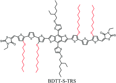 |
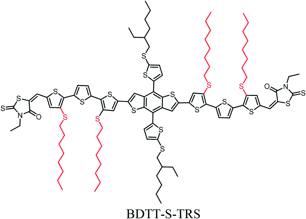
| | Scheme 1 Chemical structure of BDTT-S-TRS. | |
2. Experimental section
2.1. Materials characterization
Cyclic voltammetry was performed on a Zahner IM6e electrochemical workstation with a three-electrode system in a 0.1 M [Bu4N]PF6 acetonitrile solution at a scan rate of 100 mV s−1. A glassy carbon coated with BDTT-S-TRS film was used as the working electrode. A Pt wire was used the counter electrode and Ag/Ag+ was used as the reference electrode. The ferrocene/ferrocenium redox couple was used as the external standard and its redox potential is 0.06 V versus Ag/Ag+. The HOMO and LUMO energy levels were calculated from the onset of the oxidation and reduction potentials of BDTT-S-TRS using the following equations: HOMO = −e(φox + 4.74) (eV); LUMO = −e(φred + 4.74) (eV), respectively.
2.2. Device fabrication and characterization
The devices with a traditional structure of indium tin oxide (ITO)/poly(3,4-ethylenedioxythiophene)![[thin space (1/6-em)]](https://www.rsc.org/images/entities/char_2009.gif) :poly(styrenesulfonate) (PEDOT:PSS)/active layer/Ca/Al were fabricated and characterized in an N2-filled glove-box. Fullerene derivative [6,6]-phenyl-C71-butyric acid methyl ester (PC71BM) was employed as the acceptor material (A) to blend with BDTT-S-TRS as the donor material (D) in chloroform. The PEDOT:PSS layer was deposited by spin-coating on top of a pre-cleaned ITO-coated glass substrate. And then, the active layer was spin-coated on the PEDOT:PSS layer from a blend solution. A 10 nm Ca layer and a 100 nm Al layer were subsequently subjected to evaporation though a shadow mask to define the active area (2 × 2 mm2) of the devices and form the top anode. The current density–voltage (J–V) measurement of the devices was conducted using a Keithley 2450 source-meter under a 1 sun, AM 1.5 G spectrum from a solar simulator (AAA grade). The EQE was measured by using a QE-R3011 solar cell spectral response measurement system (Enli Technology Co., Ltd.). The light intensity at each wavelength was calibrated by a standard single-crystal Si solar cell.
:poly(styrenesulfonate) (PEDOT:PSS)/active layer/Ca/Al were fabricated and characterized in an N2-filled glove-box. Fullerene derivative [6,6]-phenyl-C71-butyric acid methyl ester (PC71BM) was employed as the acceptor material (A) to blend with BDTT-S-TRS as the donor material (D) in chloroform. The PEDOT:PSS layer was deposited by spin-coating on top of a pre-cleaned ITO-coated glass substrate. And then, the active layer was spin-coated on the PEDOT:PSS layer from a blend solution. A 10 nm Ca layer and a 100 nm Al layer were subsequently subjected to evaporation though a shadow mask to define the active area (2 × 2 mm2) of the devices and form the top anode. The current density–voltage (J–V) measurement of the devices was conducted using a Keithley 2450 source-meter under a 1 sun, AM 1.5 G spectrum from a solar simulator (AAA grade). The EQE was measured by using a QE-R3011 solar cell spectral response measurement system (Enli Technology Co., Ltd.). The light intensity at each wavelength was calibrated by a standard single-crystal Si solar cell.
Mobility measurement.
The hole and electron mobilities were calculated by using the space-charge-limited current (SCLC) method.35,36| | 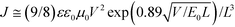 |
(1)
|
where ε is the dielectric constant of the polymers, ε0 is the permittivity of a vacuum, μ0 is the zero-field mobility, E0 is the characteristic field, J is the current density, and L is the thickness of the film.
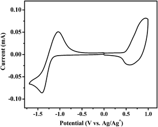
2.3. Synthesis
The monomer of BDTT-S was synthesized by a literature method.31 The general synthetic routes towards all of the new compounds are outlined in Scheme 2.
 |
| | Scheme 2 Synthetic route of BDTT-S-TRS. | |
Thiophene-3-thiol (1).
A solution of 3-bromothiophene (7.26 mL, 75 mmol) in 100 mL of dry diethyl ether was stirred at −78 °C, then 31 mL (75 mmol) of n-BuLi was added dropwise to the mixture for 0.5 h. After stirring at −78 °C for 3 hours, 2.4 g of sulfur powder was added to the mixture and kept stirred at that temperature for 0.5 h. And then the solution was warmed to room temperature to react continuously overnight. Afterwards, the mixture was poured into ice water (200 mL), neutralized with a sodium hydroxide solution and then extracted with diethyl ether. The organic layer was washed with water three times and dried over MgSO4. After removing the solvent, the crude product was used for the next step without further purification.
3-(Octylthio)thiophene (2).
Compound 1 (3.6 g, 31 mmol) and potassium tert-butoxide (6.95 g, 62 mmol) were loaded into a flask with 100 mL of ethanol and stirred at 0 °C, and then 6.0 g of 1-bromooctane was added slowly into the mixture. After being refluxed for 2 h, the reaction mixture was poured into water and extracted with ether. The organic layer was washed with water three times and dried over MgSO4. After removal of the solvent, the crude reaction mixture was subjected to column chromatography on silica gel using petroleum ether as the eluent to afford compound 2 (4.87 g, yield 69%) as a colorless oil.
1H NMR (400 MHz, CDCl3): δ (ppm) 7.31–7.30 (d, 1H), 7.11 (s, 1H), 7.01 (d, 1H), 2.86–2.82 (m, 2H), 1.62–0.87 (m, 15H). 13C NMR (100 MHz, CDCl3), δ (ppm): 132.45, 129.61, 125.94, 122.73, 35.32, 31.85, 29.44, 29.23, 29.19, 28.77, 22.71, 14.16.
2-Bromo-3-(octylthio)thiophene (3).
Compound 2 (4.87 g, 21 mmol) was dissolved in chloroform and acetic acid (60 mL, 1:1, v/v) and stirred at 0 °C. N-Bromosuccinimide (3.9 g, 22 mmol) was added in small portions. After being stirred for 12 h at room temperature, the reaction mixture was poured into water and extracted with CH2Cl2. The organic layer was washed with water three times and dried over MgSO4. After removal of the solvent, the crude reaction mixture was subjected to column chromatography on silica gel using petroleum ether as the eluent to afford compound 3 (5.22 g, yield 81%) as a light-yellow oil.
1H NMR (400 MHz, CDCl3): δ (ppm) 7.26–7.25 (d, 1H), 6.93–6.92 (d, 1H), 2.86–2.83 (m, 2H), 1.60–0.87 (m, 15H). 13C NMR (100 MHz, CDCl3), δ (ppm): 133.13, 130.10, 125.83, 113.60, 35.12, 31.77, 29.56, 29.14, 29.09, 28.58, 22.63, 14.09.
3,3′′-Bis(octylthio)-2,2′![[thin space (1/6-em)]](https://www.rsc.org/images/entities/b_char_2009.gif) :5′,2′′-terthiophene (4).
In a 100 mL flask, compound 3 (5.22 g, 17 mmol) and 2,5-bis(trimethylstannyl)thiophene (3.1 g, 7.7 mmol) were dissolved in 40 mL of toluene with 0.5 g of Pd(PPh3)4 as the catalyst. The solution was heated to reflux and stirred for 24 h under argon protection. Then, the reactant was poured into water (100 mL) and extracted with chloroform (50 mL × 3). The combined organic layer was washed with water three times and then dried over MgSO4. After removal of the solvent, the reactant was purified by column chromatography on silica gel using petroleum ether as the eluent to afford compound 4 (2.8 g, yield 68%) as a yellow oil.
:5′,2′′-terthiophene (4).
In a 100 mL flask, compound 3 (5.22 g, 17 mmol) and 2,5-bis(trimethylstannyl)thiophene (3.1 g, 7.7 mmol) were dissolved in 40 mL of toluene with 0.5 g of Pd(PPh3)4 as the catalyst. The solution was heated to reflux and stirred for 24 h under argon protection. Then, the reactant was poured into water (100 mL) and extracted with chloroform (50 mL × 3). The combined organic layer was washed with water three times and then dried over MgSO4. After removal of the solvent, the reactant was purified by column chromatography on silica gel using petroleum ether as the eluent to afford compound 4 (2.8 g, yield 68%) as a yellow oil.
1H NMR (400 MHz, CDCl3) δ (ppm): 7.32 (s, 2H), 7.18–7.17 (d, 2H), 7.05–7.03 (d, 2H), 2.88–2.84 (m, 4H), 1.63–0.83 (m, 30H).
5-Bromo-3,3′′-bis(octylthio)-2,2′:5′,2′′-terthiophene (5).
Compound 4 (2.8 g, 5.2 mmol) was dissolved in chloroform and acetic acid (60 mL, 1:1, v/v) and stirred at 0 °C. N-Bromosuccinimide (0.97 g, 5.5 mmol) was added in small portions. After being stirred for 12 h at room temperature, the reaction mixture was poured into water and extracted with CH2Cl2. The organic layer was washed with water three times and dried over MgSO4. After removing the solvent, the crude reaction mixture was subjected to column chromatography on silica gel using petroleum ether as the eluent to afford compound 5 (2.1 g, yield 65%) as a yellow oil.
1H NMR (400 MHz, CDCl3) δ (ppm): 7.29–7.28 (d, 1H), 7.22–7.21 (d, 1H), 7.19–7.18 (d, 1H), 7.04–7.03 (d, 1H), 6.99 (s, 1H), 2.87–2.82 (m, 4H), 1.62–0.85 (m, 30H). 13C NMR (100 MHz, CDCl3), δ (ppm): 137.53, 136.45, 135.55, 134.66, 134.33, 132.22, 128.33, 126.11, 125.83, 123.36, 119.60, 109.85, 36.35, 36.23, 31.80, 29.61, 29.56, 29.18, 29.17, 29.13, 28.75, 28.71, 22.65, 14.10.
5′′-Bromo-3,3′′-bis(octylthio)-[2,2′:5′,2′′-terthiophene]-5-carbaldehyde (6).
Dry N,N-dimethylformamide (DMF) (3 mL) was added dropwise to POCl3 (4 mL) and the mixture was stirred at 0 °C. After stirring at 0 °C for 0.5 h, 2.1 g of compound 5 (3.4 mmol) in 1,2-dichloroethane (30 mL) was added to the mixture which was stirred at 90 °C for 12 h. Afterwards, the mixture was poured into ice water (200 mL), neutralized with NaHCO3 and then extracted with CH2Cl2. The organic layer was washed with water three times and dried over MgSO4. After removal of the solvent, the residue was subjected to column chromatography on silica gel using a mixture of petroleum ether and CH2Cl2 (5:1) as the eluent to afford the target product as a yellow oil (1.3 g, yield: 60%).
1H NMR (400 MHz, CDCl3): δ (ppm) 9.82 (s, 1H), 7.68 (s, 1H), 7.49 (s, 1H), 7.26–7.25 (d, 1H), 7.01–7.01 (d, 1H), 2.89–2.86 (m, 4H), 1.62–0.87 (m, 30H). 13C NMR (100 MHz, CDCl3), δ (ppm): 181.94, 145.27, 141.24, 139.30, 137.53, 136.58, 134.86, 134.25, 129.49, 129.39, 128.05, 126.16, 110.85, 36.46, 36.36, 31.76, 31.57, 29.53, 29.48, 29.15, 29.11, 29.09, 28.70, 28.68, 22.62, 14.10, 14.06.
Synthesis of compound 7.
In a 100 mL flask, compound 3 (1.3 g, 2 mmol) and BDTT-S (0.89 g, 0.9 mmol) were dissolved in 40 mL of toluene with 70 mg of Pd(PPh3)4 as the catalyst. The solution was heated to reflux and stirred for 24 h under argon protection. Then, the reactant was poured into water (100 mL) and extracted with chloroform (50 mL × 3). The combined organic layer was washed with water three times and then dried over MgSO4. After removal of the solvent, the reactant was purified by column chromatography on silica gel using petroleum ether and CH2Cl2 (1:1, v/v) as the eluent to afford compound 7 (1.0 g, yield 65%) as a red solid.
1H NMR (400 MHz, CDCl3): δ (ppm) 9.78 (s, 2H), 7.64 (s, 2H), 7.52 (s, 2H), 7.48–7.47 (d, 2H), 7.34–7.33 (d, 2H), 7.31–7.30 (d, 2H), 7.27 (s, 2H), 7.15 (s, 2H), 3.03–3.01 (d, 4H), 2.93–2.87 (m, 8H), 1.65–1.25 (m, 66H), 0.99–0.85 (m, 24H). 13C NMR (100 MHz, CDCl3), δ (ppm): 181.82, 145.27, 141.27, 141.18, 139.09, 138.63, 138.18, 137.19, 137.10, 135.23, 134.86, 134.64, 132.31, 130.15, 129.91, 129.25, 128.51, 128.01, 126.08, 122.87, 119.03, 109.99, 43.47, 39.34, 36.41, 36.37, 31.77, 29.52, 29.16, 29.12, 28.78, 28.75, 25.45, 22.96, 22.62, 14.14, 14.06, 10.95. MALDI-TOF MS: calcd. for C92H118N2O2S16m/z = 1768.96; found 1768.38. Melting point (DSC): ≈166 °C, crystallizes at ≈135 °C.
Synthesis of BDTT-S-TRS.
Compound 7 (0.32 g, 0.18 mmol) was dissolved in a solution of dry CHCl3 (50 mL) and three drops of piperidine, and then 3-ethylrhodanine (0.58 mg, 3.6 mmol) was added, and the resulting solution was stirred and refluxed for 12 h under argon. The reaction mixture was then extracted with CHCl3, washed with water and dried over MgSO4. After removal of the solvent, the residue was subjected to column chromatography on silica gel using a mixture of CH2Cl2 and petroleum ether (1:1, v/v) as the eluent to afford BDTT-S-TRS as a brown solid (0.27 g, yield: 72%).
1H NMR (400 MHz, CDCl3): δ (ppm) 7.64 (s, 2H), 7.47 (s, 2H), 7.40–7.39 (d, 2H), 7.34–7.33 (d, 2H), 7.29–7.27 (m, 4H), 7.23 (s, 2H), 7.12 (s, 2H), 4.17–4.15 (m, 4H), 3.06–3.04 (m, 4H), 2.93–2.90 (m,8H), 1.69–1.28 (m, 66H), 1.02–0.85 (m, 30H). 13C NMR (100 MHz, CDCl3), δ (ppm): 191.54, 166.99, 142.45, 141.31, 138.68, 138.42, 138.14, 137.64, 137.22, 137.12, 135.52, 135.08, 134.53, 134.44, 132.13, 130.70, 130.05, 130.01, 128.50, 127.22, 126.15, 123.62, 122.86, 121.41, 118.93, 43.63, 39.83, 39.56, 36.42, 36.27, 32.30, 31.71, 29.58, 29.08, 28.83, 28.75, 25.60, 22.89, 22.52, 13.98, 13.89, 12.12, 10.91. MALDI-TOF MS: calcd. For C102H128N2O2S20m/z = 2055.42; found 2054.77. Melting point (DSC): ≈230 °C, crystallizes at ≈210 °C.
3. Results and discussion
3.1. Physicochemical properties
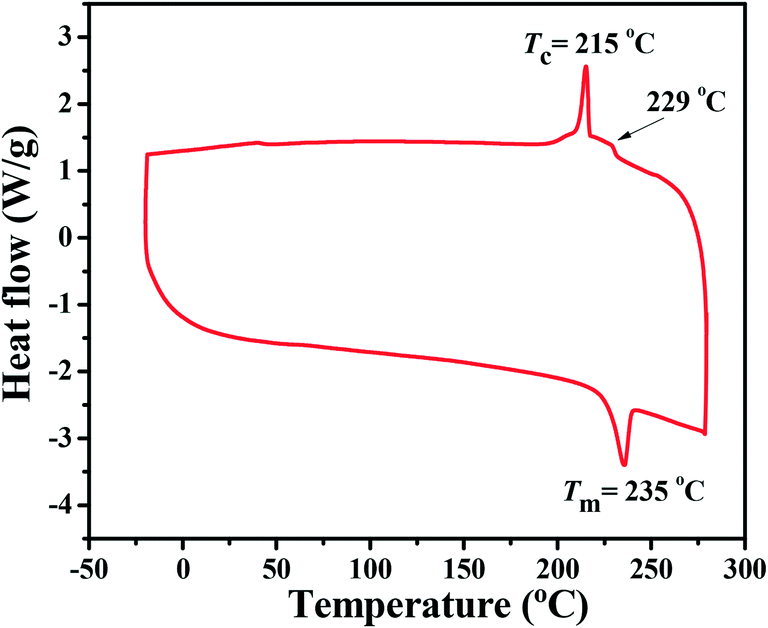
BDTT-S-TRS shows good solubility in common organic solvents, such as chloroform, chlorobenzene, etc. The differential scanning calorimetry (DSC) thermogram of BDTT-S-TRS (see Fig. 1) exhibits an endothermic peak at ≈235 °C and an exothermic peak at ≈215 °C, indicating the crystalline nature of BDTT-S-TRS. The minor transition at 229 °C indicates the phase change of BDTT-S-TRS.27
 |
| | Fig. 1 DSC thermogram (obtained from the second heating scan) of BDTT-S-TRS under an inert nitrogen atmosphere at a scan rate of 10 °C min −1 from −20 to 300 °C. | |
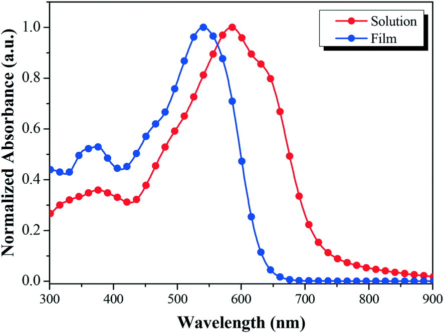
Fig. 2 shows the absorption profiles of BDTT-S-TRS in a chloroform solution and in a thin film. The BDTT-S-TRS solution displays an absorption maximum at 541 nm with a high extinction coefficient of 1.02 × 10⁵ M−1 cm−1. The absorption band of the BDTT-S-TRS film is significantly red-shifted with its absorption edge extending from 635 nm in the solution to 725 nm in the solid film, corresponding to an optical bandgap (Eg) of 1.71 eV, which is slightly lower than its analogue BDTT-S-TR (Eg = 1.73 eV).16 This indicates that the introduction of alkylthio side chains in the π-conjugated backbone of the molecule is also beneficial to red-shift the absorption spectrum to some extent. In comparison with BDTT-S-TR, BDTT-S-TRS exhibits an inconspicuous vibronic shoulder at ∼630 nm, indicating the weaker π–π stacking between the molecule backbones.
 |
| | Fig. 2 Normalized UV-vis absorption spectra of BDTT-S-TRS in chloroform solution and in thin film. | |
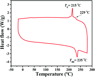
Cyclic voltammetry was carried out to measure the HOMO and LUMO (lowest unoccupied molecular orbital) energy levels of BDTT-S-TRS.37 The onset oxidation potential (φox) and the onset reduction potential (φred) of BDTT-S-TRS are 0.51 V and −1.21 V vs. Ag/Ag+, respectively (Fig. 3). Thus, the HOMO and LUMO energy levels are −5.22 eV and −3.53 eV, respectively, as listed in Table 1. Due to the effect of alkylthio side-chains, the HOMO level of BDTT-S-TRS is down-shifted slightly compared to that of BDTT-S-TR (HOMO = −5.18 eV).
 |
| | Fig. 3 Cyclic voltammograms of a BDTT-S-TRS film on a glassy carbon electrode in a 0.1 mol L−1 Bu4NPF6 acetonitrile solution at a scan rate of 100 mV s−1. | |
Table 1 Absorption spectral properties and electronic energy levels of BDTT-S-TRS
|
|
λ
max (nm) |
E
optg [eV] |
HOMO [eV] |
LUMO [eV] |
E
cvg [eV] |
| Solution |
Film |
|
BDTT-S-TRS
|
541 |
586 |
630 |
1.71 |
−5.22 |
−3.53 |
1.72 |
|
BDTT-S-TR
16
|
506 |
588 |
632 |
1.73 |
−5.18 |
−3.25 |
1.93 |
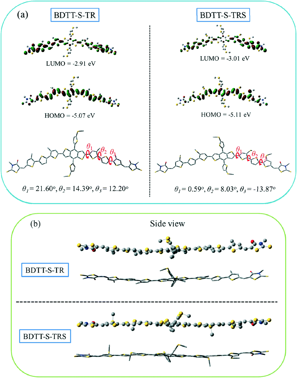
The electronic distribution and geometrical configuration of BDTT-S-TR and BDTT-S-TRS were provided by density functional theory (DFT) calculations at the B3LYP/6-31G (d,p) level to further understand the behavior of the alkylthio side-chains in the molecular system. As shown in Fig. 4a, the two molecules exhibit similar electron density distributions at the LUMO levels and HOMO levels, while the calculated HOMO level of BDTT-S-TRS is slightly lower (by 0.04 eV) than that of BDTT-S-TR. In comparison with BDTT-S-TR, smaller simulation dihedral torsion angles (θ1, θ2, and θ3) of the C–C single bond between the adjacent aromatic units are observed from BDTT-S-TRS, suggesting that the conjugated back bone planarity of BDTT-S-TRS is better than that of BDTT-S-TR. Moreover, the molecular geometry of BDTT-S-TRS shows a more linear backbone conformation from the side view than that of BDTT-S-TR. The results indicate that the introduction of alkylthio side-chains in the π-conjugated backbone has effectively down-shifted the molecular HOMO level and enhanced the conjugated planarity of the resulting molecule.
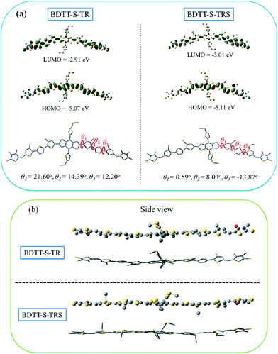 |
| | Fig. 4 (a) LUMO and HOMO energy levels and molecular geometry with the simulated dihedral angles of BDTT-S-TR and BDTT-S-TRS calculated by DFT/B3LYP/6-31G (d,p) with methyl groups replacing the alkyl substituents to simplify the calculations. (b) Side view of the optimized geometry of BDTT-S-TR and BDTT-S-TRS. | |
3.2. Photovoltaic properties
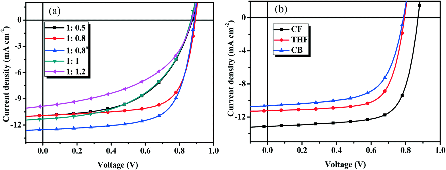
To optimize the device performance, the effect of D/A weight ratios on the photovoltaic performance was carefully investigated. Fig. 5a shows the current density–voltage (J–V) curves and Table 2 lists the main photovoltaic performance parameters of the OSCs with different D/A weight ratios under the illumination of AM 1.5 G at 100 mW cm−2. As shown in Table 2, the Voc (0.86–0.89 V) and Jsc (10.19–11.32 mA cm−2) values do not change when the D/A ratio is changed from 1:0.5 to 1:1.2 (w/w), while the FF (from 0.487 to 0.689) values are very different. The optimal D/A weight ratio of BDTT-S-TRS:PC71BM was found to be 1:0.8 (w/w), and the corresponding device exhibited a PCE of 6.72%, with a Voc of 0.89 V, a Jsc of 10.93 mA cm−2, and a FF of 0.689. By using poly[(9,9-bis(3′-(N,N-dimethylamino)propyl)-2,7-fluorene)–alt−2,7-(9,9-dioctylfluorene)] (PFN) instead of Ca as a cathode interlayer, a higher Jsc value of 12.53 mA cm−2 was achieved, leading to an improved PCE of 7.51%.
 |
| | Fig. 5
J–V curves of (a) the BDTT-S-TRS based devices with different D/A weight ratios, and (b) BDTT-S-TRS:PC71BM (1:0.8, w/w) with SVA treatment. | |
Table 2 Photovoltaic performance of the OSCs based on BDTT-S-TRS:PC71BM with different D/A weight ratios under illumination of AM 1.5 G at 100 mW cm−2
| D/A weight ratio |
V
oc [V] |
J
sc [mA cm−2] |
FF [%] |
PCE [%] |
PCEaveb [%] |
|
By using PFN instead of Ca as a cathode interlayer.
PCEave stands for the average PCE obtained from 6 devices.
|
| 1:0.5 |
0.88 |
10.92 |
52.8 |
5.05 |
4.86 ± 0.22 |
| 1:0.8 |
0.89 |
10.93 |
68.9 |
6.72 |
6.65 ± 0.14 |
| 1:0.8a |
0.89 |
12.53 |
67.5 |
7.51 |
7.38 ± 0.11 |
| 1:1 |
0.87 |
11.32 |
51.0 |
5.00 |
4.87 ± 0.21 |
| 1:1.2 |
0.86 |
10.19 |
48.7 |
4.28 |
4.10 ± 0.13 |
To further improve the photovoltaic performance, solvent vapor annealing (SVA) was carried out to optimize the morphology of the blend film. Fig. 5b shows the J–V curves and Table 3 lists the main photovoltaic performance parameters of the OSCs with different SVA treatments under illumination of AM 1.5 G at 100 mW cm−2. As show in Table 3, by exposing the active layer to chloroform (CF) vapor for 30 s, the Jsc and FF values were improved to 11.31 mA cm−2 and 0.71, respectively, delivering a higher PCE of 7.03%. The replacement of Ca with PFN as a cathode interlayer leads to a significant improvement of Jsc of 13.14 mA cm−2, leading to a higher PCE of 8.07%, with a Voc of 0.87 V, and a notable FF of 0.705. No positive effect on the photovoltaic performance was observed from the devices with tetrahydrofuran (THF) or chlorobenzene (CB) SVA treatments. The highest PCE of 6.23% was obtained by THF SVA treatment, with Voc = 0.79 V, Jsc = 11.24 mA cm−2, and FF = 0.699. By performing the CB SVA treatment, the device exhibited its best performance with a PCE = 5.33%, Voc = 0.79 V, Jsc = 10.65 mA cm−2, and FF = 0.639. Due to the fact that Voc depends on several factors (such as the bulkiness of side chains, morphology of the active layer, etc.) besides the HOMO level of the donor material,38–40 unexpected lower Voc values (compared with BDTT-S-TR based devices, Voc = 0.95–0.97 V) were obtained from BDTT-S-TRS based devices in this case.
Table 3 Photovoltaic parameters of the OSCs based on BDTT-S-TRS:PC71BM (1:0.8, w/w) with SVA for different times, under illumination of AM 1.5 G at 100 mW cm−2
| SVA solvent |
SVA time (s) |
V
oc [V] |
J
sc [mA cm−2] |
FF [%] |
PCE [%] |
PCEaveb [%] |
|
By using PFN instead of calcium as a cathode interlayer.
PCEave stands for the average PCE obtained from 12 devices.
|
| CF |
15 |
0.87 |
10.58 |
69.8 |
6.57 |
6.42 ± 0.11 |
| 15a |
0.87 |
13.14 |
70.5 |
8.07 |
7.98 ± 0.12 |
| 30 |
0.88 |
11.31 |
71.0 |
7.03 |
6.87 ± 0.32 |
| 30a |
0.87 |
13.73 |
67.5 |
7.96 |
7.85 ± 0.16 |
| 60 |
0.86 |
11.16 |
65.9 |
6.34 |
6.09 ± 0.23 |
| 90 |
0.86 |
11.04 |
68.9 |
6.54 |
6.25 ± 0.22 |
| 120 |
0.87 |
10.25 |
62.7 |
5.56 |
5.47 ± 0.23 |
| THF |
15 |
0.79 |
11.24 |
69.9 |
6.23 |
6.10 ± 0.10 |
| 30 |
0.76 |
10.89 |
72.5 |
5.98 |
5.67 ± 0.25 |
| 60 |
0.80 |
10.67 |
72.3 |
6.17 |
5.97 ± 0.24 |
| CB |
60 |
0.79 |
10.65 |
63.6 |
5.33 |
5.18 ± 0.11 |
| 120 |
0.78 |
10.54 |
58.9 |
4.85 |
4.63 ± 0.23 |
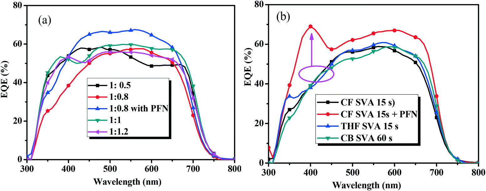
The external quantum efficiency (EQE) curves of the optimal devices based on BDTT-S-TRS are shown in Fig. 6. As shown by the EQE curves, broad wavelengths ranging from 300 to 700 nm are observed for all the devices based on BDTT-S-TRS. The EQE values of the BDTT-S-TRS:PC71BM (1:0.8, w/w) based device with or without SVA treatment are ∼60% in the wavelength range of 500–600 nm, demonstrating a high efficiency of light harvesting and charge carrier collection. The peak value was enhanced to over 65% by replacing Ca with PFN as a cathode interlayer, suggesting a better photo-response which explains the higher Jsc value of the corresponding device.
 |
| | Fig. 6 EQE curves of (a) the BDTT-S-TRS based devices with different D/A weight ratios, and (b) BDTT-S-TRS:PC71BM (1:0.8, w/w) with SVA treatment. | |
3.3. Mobility measurements
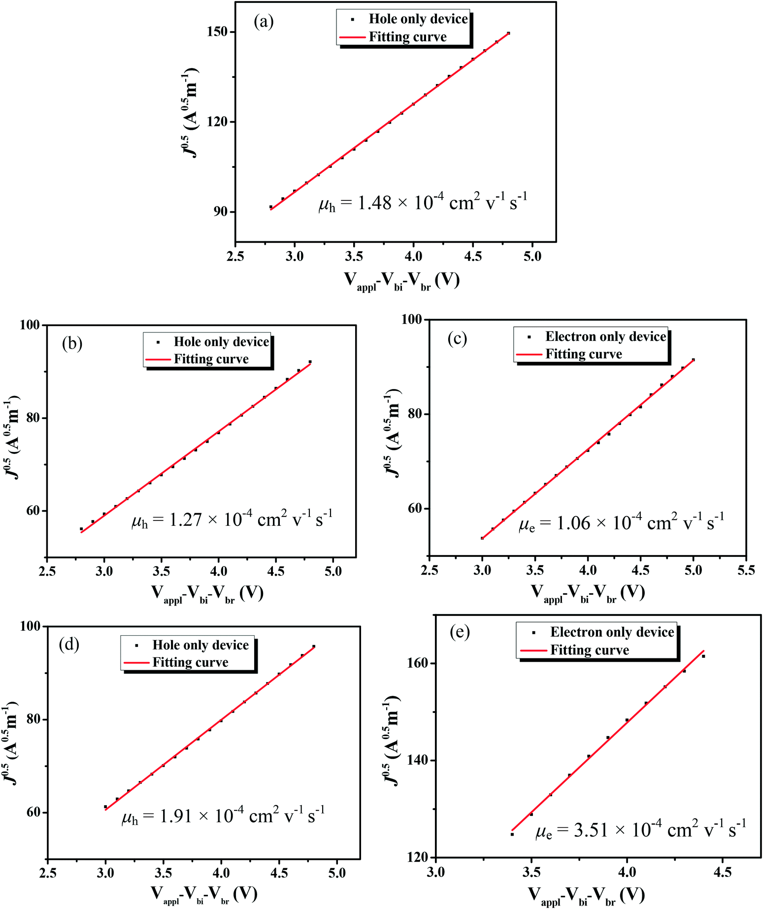
The charge-carrier mobilities of the photovoltaic materials are critical for OSC devices. To investigate the charge-carrier mobilities of the BDTT-S-TRS-based active layer, the hole-only device with a structure of ITP/PEDOT:PSS/ BDTT-S-TRS:PC71BM (1:0.8, w/w) (or pure BDTT-S-TRS)/MoO3/Au was constructed for hole mobility measurements, and the electron-only device with a device structure of ITO/ZnO/BDTT-S-TRS:PC71BM (1:0.8, w/w)/Al was fabricated for electron mobility measurement by the space-charge-limited-current (SCLC) method. As shown in Fig. 7a, the pure BDTT-S-TRS film exhibited a high hole mobility of 1.48 × 10⁻⁴ cm2 V−1 s−1. The BDTT-S-TRS:PC71BM (1:0.8, w/w) blend film without any extra treatment showed a hole mobility of 1.27 × 10⁻⁴ cm2 V−1 s−1 and an electron mobility of 1.06 × 10⁻⁴ cm2 V−1 s−1, respectively. After CF SVA treatment for 15 s, a slightly higher hole mobility of 1.91 × 10⁻⁴ cm2 V−1 s−1 and a higher electron mobility of 3.51 × 10⁻⁴ cm2 V−1 s−1 were observed, indicating the positive effect of the CF SVA treatment on the improvement of the charge-carrier mobilities of the blend film. The relatively high and balanced hole and electron mobilities of the blend film are beneficial for achieving the high FF of the devices.
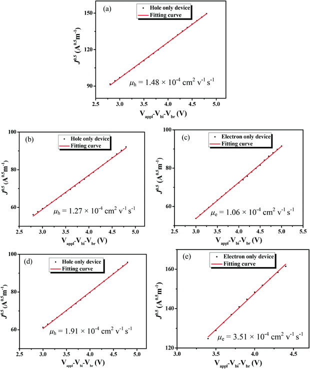 |
| | Fig. 7
J
0.5
vs. (Vapp–Vbi–Vbr) plots of (a) the pristine BDTT-S-TRS film; (b) hole-only devices and (c) electron-only devices of the BDTT-S-TRS:PC71BM (1:0.8, w/w) blend film; and (d) hole-only devices and (e) electron only devices of the BDTT-S-TRS:PC71BM (1:0.8, w/w) blend film with CF SVA for 15 s. | |
3.4. XRD and morphology analysis
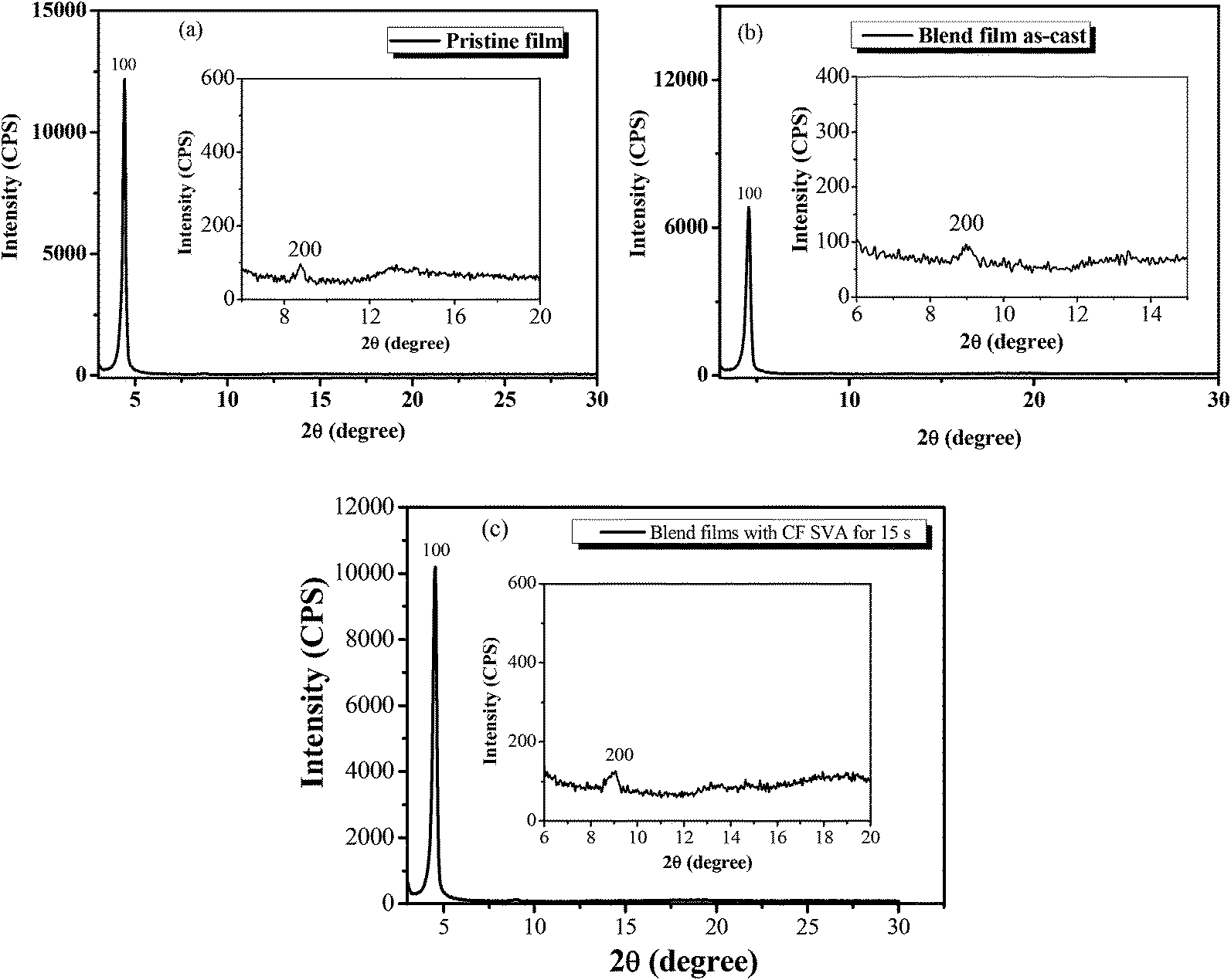
The crystalline nature of the BDTT-S-TRS film and the BDTT-S-TRS:PC71BM (1:0.8) blend film without or with CF SVA treatment was characterized by X-ray diffraction (XRD) analysis. As shown in Fig. 8a, the BDTT-S-TRS film exhibits high crystallinity with a strong (100) diffraction peak at 2θ = 4.42°, corresponding to a d100-spacing of 20.0 Å, and a weak (200) diffraction peak at 2θ =8.76°. A clear and strong diffraction (100) peak at 2θ = 4.56° (Fig. 8b) can also be observed in the BDTT-S-TRS:PC71BM (1:0.8, w/w) as-cast blend films, corresponding to a d100-spacing of 19.3 Å, respectively. By treating with CF SVA for 15 s, the diffraction intensity of the blend film exhibited a stronger 100 reflection at 2θ = 4.54° (Fig. 8c), corresponding to a d100-spacing of 19.4 Å, indicating the positive effect of CF SVA in improving the crystalline properties of the blend film.
 |
| | Fig. 8 XRD patterns of (a) the BDTT-S-TRS film, (b) BDTT-S-TRS:PC71BM (1:0.8, w/w) blend films, and (c) BDTT-S-TRS:PC71BM (1:0.8, w/w) blend films with CF SVA treatment for 15 s. | |
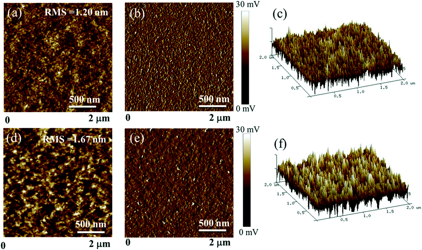
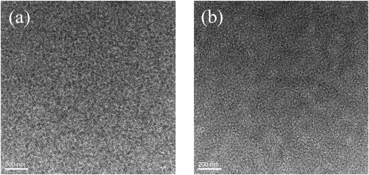
The surface and bulk morphologies of the BDTT-S-TRS:PC71BM (1:0.8, w/w) blend films were examined by atomic force microscopy (AFM) and transmission electron microscopy (TEM). As shown in Fig. 9, both the BDTT-S-TRS:PC71BM (1:0.8, w/w) blend films without or with CF SVA treatment show rather flat and uniform surfaces. The root-mean-square (RMS) roughness value of the blend film without extra-treatment is 1.20 nm. After being processed with CF SVA for 15 s, the surface of the blend films became rough with an RMS value of 1.67 nm. The TEM images of the two blend films gave a similar good bicontinuous D/A interpenetrating network and a well-developed homogeneous morphology with nanosize segregated crystallites (as shown in Fig. 10), which should favor high efficiency exciton dissociation and charge transportation, and thus high FF values can be achieved.
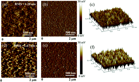 |
| | Fig. 9 (a) AFM topography image, (b) the corresponding phase image and (c) 3D topography image of the BDTT-S-TRS:PC71BM (1:0.8, w/w) blend films without any treatment, respectively; (d) AFM topography image, (e) the corresponding phase image and (f) 3D topography image of the BDTT-S-TRS:PC71BM (1:0.8, w/w) blend films with CF SVA treatment for 15 s, respectively. | |
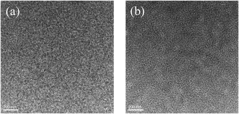 |
| | Fig. 10 TEM images of the BDTT-S-TRS:PC71BM (1:0.8, w/w) blend films (a) without any treatment and (b) with CF SVA treatment for 15 s. | |
4. Conclusion
In summary, we developed a new small molecule with an alkylthio side-chain in its conjugated backbone as a donor material for OSCs. In comparison with its alkyl side-chains counterpart, the engineering of an alkylthio side-chain in the molecular conjugated backbone is beneficial to achieve a linear backbone conformation, slightly red-shift the absorption spectrum, and down-shift the HOMO energy level of the resulting molecule. The optimized OSC device based on BDTT-S-TRS exhibited a PCE of 8.07%, with a Voc of 0.87 V, a Jsc of 13.14 mA cm−2, and a notable FF of 0.705. The relatively high charge-carrier mobilities and well-developed morphological features of the blend film enable the high Jsc and FF of the resulting devices. This preliminary work further exploits the capability of alkylthio side-chains in tuning the physicochemical properties of the small-molecule OSCs. It is believed that there is still great potential for the BDTT-S-TRS-based devices to achieve higher PCEs via controlling and optimizing the morphology of the active layer to realize high Voc values (consistent with the low-lying HOMO energy level). More importantly, the results demonstrate that the strategy of introducing an alkylthio side-chain in the molecular conjugated backbone could obtain both a deep HOMO level and a low optical band-gap, which should be in favor of realizing high photovoltaic performance.
Conflicts of interest
There are no conflicts to declare.
Acknowledgements
This work was supported by the National Natural Science Foundation of China (51603136, 91633301, 91333204), the Jiangsu Provincial Natural Science Foundation (Grant no. BK20150327), the Natural Science Foundation of the Jiangsu Higher Education Institutions of China (Grant no. 15KJB430028), the Priority Academic Program Development of Jiangsu Higher Education Institutions (PAPD), and the Project Funded by the China Postdoctoral Science Foundation (Grant no. 2015 M581855, 2017 T100395).
References
- G. Li, R. Zhu and Y. Yang, Nat. Photonics, 2012, 6, 153–161 CrossRef CAS.
- Y. Li, Acc. Chem. Res., 2012, 45, 723–733 CrossRef CAS PubMed.
- A. J. Heeger, Adv. Mater., 2013, 26, 10–27 CrossRef PubMed.
- L. Ye, S. Zhang, L. Huo, M. Zhang and J. Hou, Acc. Chem. Res., 2014, 47, 1595–1603 CrossRef CAS PubMed.
- Y. Cui, H. Yao, B. Gao, Y. Qin, S. Zhang, B. Yang, C. He, B. Xu and J. Hou, J. Am. Chem. Soc., 2017, 139, 7302–7309 CrossRef CAS PubMed.
- W. Zhao, S. Li, H. Yao, S. Zhang, Y. Zhang, B. Yang and J. Hou, J. Am. Chem. Soc., 2017, 139, 7148–7151 CrossRef CAS PubMed.
- Y. Qin, Y. Chen, Y. Cui, S. Zhang, H. Yao, J. Huang, W. Li, Z. Zheng and J. Hou, Adv. Mater., 2017, 29, 1606340 CrossRef PubMed.
- S. Li, L. Ye, W. Zhao, S. Zhang, S. Mukherjee, H. Ade and J. Hou, Adv. Mater., 2016, 28, 9423–9429 CrossRef CAS PubMed.
- F. Zhao, S. Dai, Y. Wu, Q. Zhang, J. Wang, L. Jiang, Q. Ling, Z. Wei, W. Ma, W. You, C. Wang and X. Zhan, Adv. Mater., 2017, 29, 1700144 CrossRef PubMed.
- Y. Lin, Y. Li and X. Zhan, Chem. Soc. Rev., 2012, 41, 4245–4272 RSC.
- H. Bin, L. Gao, Z.-G. Zhang, Y. Yang, Y. Zhang, C. Zhang, S. Chen, L. Xue, C. Yang, M. Xiao and Y. Li, Nat. Commun., 2016, 7, 13651 CrossRef CAS PubMed.
- S. Li, W. Liu, C.-Z. Li, M. Shi and H. Chen, Small, 2017, 13, 1701120 CrossRef PubMed.
- Y. Lin and X. Zhan, Acc. Chem. Res., 2015, 49, 175–183 CrossRef PubMed.
- Y. Chen, X. Wan and G. Long, Acc. Chem. Res., 2013, 46, 2645–2655 CrossRef CAS PubMed.
- B. Kan, M. Li, Q. Zhang, F. Liu, X. Wan, Y. Wang, W. Ni, G. Long, X. Yang, H. Feng, Y. Zuo, M. Zhang, F. Huang, Y. Cao, T. P. Russell and Y. Chen, J. Am. Chem. Soc., 2015, 137, 3886–3893 CrossRef CAS PubMed.
- C. Cui, X. Guo, J. Min, B. Guo, X. Cheng, M. Zhang, C. J. Brabec and Y. Li, Adv. Mater., 2015, 27, 7469–7475 CrossRef CAS PubMed.
- Y. Yang, Z.-G. Zhang, H. Bin, S. Chen, L. Gao, L. Xue, C. Yang and Y. Li, J. Am. Chem. Soc., 2016, 138, 15011–15018 CrossRef CAS PubMed.
- L. Yang, S. Zhang, C. He, J. Zhang, H. Yao, Y. Yang, Y. Zhang, W. Zhao and J. Hou, J. Am. Chem. Soc., 2017, 139, 1958–1966 CrossRef CAS PubMed.
- J. Wan, X. Xu, G. Zhang, Y. Li, K. Feng and Q. Peng, Energy Environ. Sci., 2017, 10, 1739–1745 CAS.
- S. D. Collins, N. A. Ran, M. C. Heiber and T.-Q. Nguyen, Adv. Energy Mater., 2017, 7, 1602242 CrossRef.
- D. Deng, Y. Zhang, J. Zhang, Z. Wang, L. Zhu, J. Fang, B. Xia, Z. Wang, K. Lu, W. Ma and Z. Wei, Nat. Commun., 2016, 7, 13740 CrossRef CAS PubMed.
- M. Li, W. Ni, X. Wan, Q. Zhang, B. Kan and Y. Chen, J. Mater. Chem. A, 2015, 3, 4765–4776 CAS.
- T.-H. Chang, C.-W. Kung, H.-W. Chen, T.-Y. Huang, S.-Y. Kao, H.-C. Lu, M.-H. Lee, K. M. Boopathi, C.-W. Chu and K.-C. Ho, Adv. Mater., 2015, 27, 7229–7235 CrossRef CAS PubMed.
- A.-C. Knall, R. S. Ashraf, M. Nikolka, C. B. Nielsen, B. Purushothaman, A. Sadhanala, M. Hurhangee, K. Broch, D. J. Harkin, J. Novák, M. Neophytou, P. Hayoz, H. Sirringhaus and I. McCulloch, Adv. Funct. Mater., 2016, 26, 6961–6969 CrossRef CAS.
- J. Mei and Z. Bao, Chem. Mater., 2013, 26, 604–615 CrossRef.
- Z.-G. Zhang and Y. Li, Sci. China: Chem., 2015, 58, 188–188 CrossRef.
- K. Sun, Z. Xiao, S. Lu, W. Zajaczkowski, W. Pisula, E. Hanssen, J. M. White, R. M. Williamson, J. Subbiah, J. Ouyang, A. B. Holmes, W. W. H. Wong and D. J. Jones, Nat. Commun., 2015, 6, 6013 CrossRef CAS PubMed.
- J.-L. Wang, K.-K. Liu, S. Liu, F. Xiao, Z.-F. Chang, Y.-Q. Zheng, J.-H. Dou, R.-B. Zhang, H.-B. Wu, J. Pei and Y. Cao, Chem. Mater., 2017, 29, 1036–1046 CrossRef CAS.
- S. Subramaniyan, H. Xin, F. S. Kim, S. Shoaee, J. R. Durrant and S. A. Jenekhe, Adv. Energy Mater., 2011, 1, 854–860 CrossRef CAS.
- C. Cui and W.-Y. Wong, Macromol. Rapid Commun., 2016, 37, 287–302 CrossRef CAS PubMed.
- C. Cui, W.-Y. Wong and Y. Li, Energy Environ. Sci., 2014, 7, 2276–2284 CAS.
- C. Cui, Z. He, Y. Wu, X. Cheng, H. Wu, Y. Li, Y. Cao and W.-Y. Wong, Energy Environ. Sci., 2016, 9, 885–891 CAS.
- X. Cheng, Q. Wan, Y. Wu, B. Guo, X. Guo, Y. Li, M. Zhang, C. Cui and Y. Li, Sol. Energy Mater. Sol. Cells, 2016, 149, 162–169 CrossRef CAS.
- Y. Wu, X. Cheng, G. Xu, Y. Li, C. Cui and Y. Li, RSC Adv., 2016, 6, 108908–108916 RSC.
- C. Melzer, E. J. Koop, V. D. Mihailetchi and P. W. M. Blom, Adv. Funct. Mater., 2004, 14, 865–870 CrossRef CAS.
- V. D. Mihailetchi, L. J. A. Koster, P. W. M. Blom, C. Melzer, B. de Boer, J. K. J. van Duren and R. A. J. Janssen, Adv. Funct. Mater., 2005, 15, 795–801 CrossRef CAS.
- Y. Li, Y. Cao, J. Gao, D. Wang, G. Yu and A. J. Heeger, Synth. Met., 1999, 99, 243–248 CrossRef CAS.
- M. D. Perez, C. Borek, S. R. Forrest and M. E. Thompson, J. Am. Chem. Soc., 2009, 131, 9281–9286 CrossRef CAS PubMed.
- K. Vandewal, K. Tvingstedt, A. Gadisa, O. Inganas and J. V. Manca, Nat. Mater., 2009, 8, 904–909 CrossRef CAS PubMed.
- H. Zhou, L. Yang and W. You, Macromolecules, 2012, 45, 607–632 CrossRef CAS.
|
| This journal is © The Royal Society of Chemistry 2018 |
Click here to see how this site uses Cookies. View our privacy policy here. 
 *a and
Yongfang
Li
*a and
Yongfang
Li