DOI:
10.1039/D1LC00614B
(Paper)
Lab Chip, 2021,
21, 4596-4607
Amplification factor in DC insulator-based electrokinetic devices: a theoretical, numerical, and experimental approach to operation voltage reduction for particle trapping†
Received
12th July 2021
, Accepted 23rd September 2021
First published on 5th November 2021
Abstract
Insulator-based microfluidic devices are attractive for handling biological samples due to their simple fabrication, low-cost, and efficiency in particle manipulation. However, their widespread application is limited by the high operation voltages required to achieve particle trapping. We present a theoretical, numerical, and experimental study that demonstrates these voltages can be significantly reduced (to sub-100 V) in direct-current insulator-based electrokinetic (DC-iEK) devices for micron-sized particles. To achieve this, we introduce the concept of the amplification factor—the fold-increase in electric field magnitude due to the presence of an insulator constriction—and use it to compare the performance of different microchannel designs and to direct our design optimization process. To illustrate the effect of using constrictions with smooth and sharp features on the amplification factor, geometries with circular posts and semi-triangular posts were used. These were theoretically approximated in two different systems of coordinates (bipolar and elliptic), allowing us to provide, for the first time, explicit electric field amplification scaling laws. Finite element simulations were performed to approximate the 3D insulator geometries and provide a parametric study of the effect of changing different geometrical features. These simulations were used to predict particle trapping voltages for four different single-layer microfluidic devices using two particle suspensions (2 and 6.8 μm in size). The general agreement between our models demonstrates the feasibility of using the amplification factor, in combination with nonlinear electrokinetic theory, to meet the prerequisites for the development of portable DC-iEK microfluidic systems.
Introduction
Insulator-based electrokinetics (iEK) is an emerging microfluidic technology where dielectric materials and interfaces determine the spatial distribution of an externally applied electric field, producing motion of fluids and particles contained therein. This principle has been exploited to design and implement microdevices for controlling the position, velocity, and concentration of biological and non-biological particles in lab-on-a-chip and point-of-care platforms.1 When direct current (DC) electric fields are applied to an iEK device (DC-iEK), they interact with the charge distributions at the interfaces of the different material phases involved. From these interactions, three main electrokinetic phenomena arise: electroosmosis (EO), electrophoresis (EP) and dielectrophoresis (DEP)—a non-uniform electric field spatial distribution is required for DEP to exist. It is, then, through the combined effect of EO, EP and DEP, that particle control (mostly trapping) is achieved. The extent to which EO and EP remain linear with the magnitude of the applied electric fields critically depends on the degree of polarization of the electric double layers (EDL) formed at the channel/liquid and particle/liquid interfaces, respectively. In the case of DEP, the exerted force on particles is dependent on their induced polarization and the gradient of the squared magnitude of the electric field, i.e., FDEP ∝ ∇(E·E). Understanding how the presence of insulators alters the distribution and magnitude of electric fields has therefore been the subject of numerous iEK studies.2,3
Until recently, DEP was considered strong enough to balance the combined effect of linear EP and EO in DC-iEK devices for particle trapping.2 Additionally, the nonlinear nature of EP (also known as EP(3) or EP of the second kind4,5) had not been posited as a possible major contributor to particle trapping phenomena.6 However, when taking such nonlinear nature into consideration, a hypothesis can be defined where the electrokinetic trapping of particles is mainly attributed to the balancing of linear EP(1) and nonlinear EP(3) kinetic components with EO flow (Fig. 1A). Exploring this path, recent studies on experimental microorganism trapping assays indicated that DEP represented about 0.89% to 5.85% of the nonlinear EP, and demonstrated that this higher order DC-iEK phenomena can be used to build an electrokinetic characterization library of cells.7 The same principle has already been used to study in more detail the electrokinetic properties and behavior of bioparticles in DC insulator-based systems.8,9 These results suggest that producing electric fields of high magnitude capable of eliciting these nonlinear responses can, in fact, be more critical to particle trapping than producing fields with high ∇(E·E).
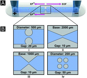 |
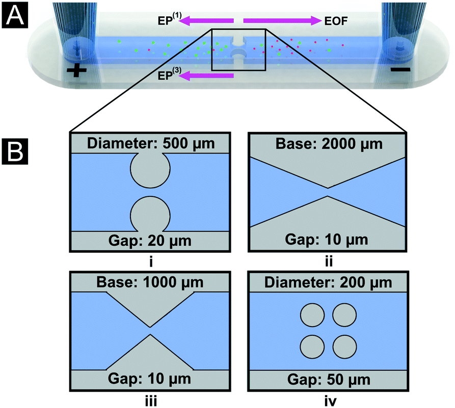
| | Fig. 1 Schematic representation of the channel designs used for particle trapping. (A) Illustration of a channel with reservoirs and the electrokinetic effects experienced by the two negatively charged particles employed in the study. Arrows represent the direction of the predominant electrokinetic components. In our system, EO flow direction is from left to right, while EP and EP(3) migration is from right to left. (B) An illustration of the four channel designs that were studied (i, circular; ii and iii, triangular; iv, multi-column), along with the design variables of the insulating posts where the gap size is the spacing between two post boundaries. | |
Typically, iEK devices use insulating structures (‘posts’) embedded in a microchannel to alter the electric field distribution produced by an electric potential difference applied across the microchannel.10 Because these structures can be readily obtained through well-known, simple, and affordable 2D soft-lithography techniques, DC-iEK devices have been applied to the trapping of a variety of bioparticles and biomolecules, including proteins, DNA, viruses, cells and cell organelles.11–13 Nonetheless, widespread adoption of DC-iEK devices has been limited by their operation voltage, which can be as high as 3000 V for manipulating polystyrene particles and 4000 V for PEGylated proteins in traditional designs.14–16 Evidently, high voltages carry several practical problems for lab-on-a-chip applications, such as electrolysis, joule heating, and complex electrical equipment,16,17 and thereby reduce the applicability of DC-iEK devices to biological systems.
Several studies have focused on reducing the operation voltage requirements in DC-iEK microfluidic systems.18–24 For instance, devices with 3D constrictions have been used to enhance the E field nonuniformity, which while effective for achieving low trapping voltages for relatively large polystyrene particles (10 μm), need to be individually micro-milled.18 Other works focusing on 2D DC-iEK devices have concentrated in maximizing the magnitude of ∇(E·E) to increase DEP, mainly seeking to explore the effect of post shape through finite element numerical simulations of the electric field distribution.19–23 This is in part because the other main controllable variable involved, namely post separation (commonly referred to as ‘gap’), is generally regarded as the limiting factor, both from a technological and parameter optimization standpoint: smaller gaps generally result in stronger fields albeit at greater fabrication complexity. Furthermore, a recent work has demonstrated that increasing the number of insulating obstacles longitudinally present in a microchannel inversely affects the magnitude of the obtained electric field, even if the same gap sizes are used for multiple columns.24 These observations suggest that the presence of dielectrics and the constriction shape they form alters the electric field distribution and magnitude nontrivially for equal gap sizes, which warrants an analysis of the expressions and scaling laws that could estimate the expected electric field enhancement in DC-iEK devices.
The present study aims to reduce the operation voltage in DC-iEK devices by building on two main observations: i) that producing high-magnitude electric fields—rather than high ∇(E·E)—elicits nonlinear EP and thereby particle trapping;6 and ii) that using single dielectric constrictions, rather than multiple columns, increases the electric field magnitude.24 Voltage reduction was therefore achieved by optimizing the geometry of DC-iEK devices. First, we introduced a device geometry consisting of a single dielectric constriction formed by two circular posts—a minimal system that captures the gap/post dimensions, and that admits analytic solutions to the electric field distribution.6 We demonstrate an improvement to this system through a sharp triangular constriction for which the solution can also be analytically approximated. Analytical expressions of the electric field allowed us to explicitly define the field magnitude enhancement—deemed the ‘amplification factor’. Although we previously introduced this concept in a recent work on DC-iEK particle trapping experiments,6 here we present for the first time how this concept allows the derivation of explicit electric field scaling laws to compare our designs. Theoretical approximations were then improved on through full numerical simulations of the complete 3D geometries of the microdevices to parametrically explore (in a more realistic model) the effects of post diameter and gap in the circular geometry (Fig. 1B, i), and triangle base and gap size (Fig. 1B, ii and iii). The numerical model was validated by experimentation with 2 and 6.8 μm polystyrene particles to confirm the reduction of trapping voltages. A segmented regression routine optimized using the least squares method was implemented to analyze the experimental fluorescence intensity and to obtain an automatic and objective determination of trapping voltages. Finally, the optimized circular and triangular geometries (Fig. 1B, i and iii) were used to evaluate the separation of the two particles by size and their performance compared to a conventional DC-iEK design (Fig. 1B, iv).25 We demonstrate that trapping voltages of ∼80 V can be attained at a standard conductivity of 20–25 μS cm−1—being, to our knowledge, the lowest trapping voltages reported to date for 2D DC-iEK microfluidic systems using particles in this size range.26 Our findings illustrate how dielectric constriction optimization can maximize the attainable E field magnitude, thereby reducing voltage requirements and enabling improved portability in DC-iEK systems.
Theory
Nonlinear electrokinetics
In this study, we use EO and EP to achieve particle manipulation in DC-iEK devices featuring a non-uniform E field spatial distribution (even with ∇(E·E) ≠ 0, we neglect DEP based on recent evidence suggesting its contribution to particle velocity in these systems is marginal).6,7 EO is the movement of a fluid with respect to a surface and EP is the movement of charged particles relative to a fluid. Both EK phenomena are affected by the interaction of solute ions and surface charges in the solid phases, which give rise to the electric double layer (EDL) of the channel walls (important for EO) and particle (important for EP).27 In the presence of a low-magnitude E field, EO and EP behave linearly with respect to the electric field and their velocity components to a first order approximation are:| | 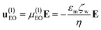 | (1) |
| |  | (2) |
where μ(1)EO and μ(1)EP are the first order electroosmotic and electrophoretic mobilities, respectively, which are functions that depend on the medium permittivity (εm), wall zeta potential (ζw), particle zeta potential (ζp), and medium viscosity (η). However, when a high-magnitude electric field is applied, it modifies the EDL of the particles by inducing a concentration polarization on the diffuse layer. Nonlinearity in the electrophoretic response is introduced by the above-mentioned surface conductance, a phenomenon known as electrokinetics of the second kind as initially described by Dukhin.5 Since then, several contributions have enabled us to better understand non-linear EK,6,28,29 where the net electrophoretic velocity u(3)EP is expressed as a third order approximation:| | | u(3)EP = μ(1)EPE + μ(3)EPE3 | (3) |
| |  | (4) |
Here, μ(3)EP represents the third-order electrophoretic mobility that depends on the first order mobilities, as well as the electrokinetic equilibrium condition (EEEC). The EEEC—a recently introduced fundamental concept that has radically shifted the perspective behind the analysis of particle manipulation in these microfluidic devices6—describes the balance between linear EO, linear EP, and nonlinear EP, and can be characterized experimentally.8 When adding these effects on the particle, the total particle velocity can be defined as:where u(1)EO is the EO component, and u(3)EP is the combination of velocities for the linear and non-linear EP effects. eqn (5) can be rewritten as:| | | up = μEOE + μ(1)EPE + μ(3)EPE3 | (6) |
Notice that eqn (6) suggests a dependence of particle velocity with the E field magnitude, which differs from previous studies that considered DEP as the predominant phenomenon—therefore focusing on optimizing ∇(E·E) yielding a non-optimal reduction in voltage.
Analytic expressions of the electric field
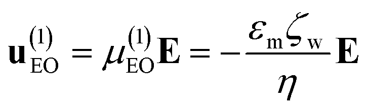
We explored two main geometries for introducing an electric field non-uniformity that allowed the capture of microparticles: i) circular posts and ii) semi-triangular-shaped posts (with rounded tips). We present two analytic solutions, which can be used to approximate the non-uniform electric field within the microfluidic devices when an external field E0ĵ is applied (see Fig. 2). Single-constriction channels were analyzed because previous studies demonstrated improved particle trapping capabilities in insulator arrays featuring a single column of posts.24 Another advantage of using single-constriction channels is that they can be approximately represented through a suitable choice of coordinate systems for which the Laplace equation ∇2ϕ = 0 is separable (typically by neglecting the third out-of-plane coordinate as an approximation).
 |
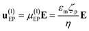
| | Fig. 2 Analytic solution of the electric field for the two geometries used. (A) Bipolar coordinate system, showing the relative position of insulator posts. (B) Electric field solution, where the colormap indicates the magnitude normalized to the applied field E0, and arrows the direction. (C) Cutline plot of the normalized electric field magnitude along the central axis in (B), showing a maximum of Ψc. (D–F) In analogy to (A–C), figures are displayed for the elliptic coordinate system. | |
Electric field solution for circular posts.
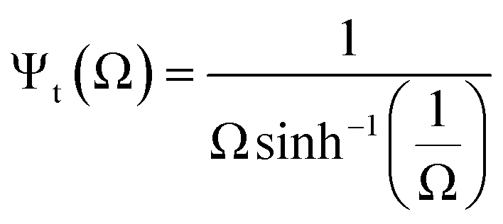
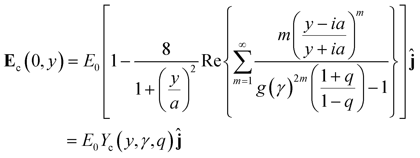
We have previously demonstrated that a circular two-post geometry admits a representation in the bipolar coordinate system (see Fig. 2A and B).6 The two posts can be approximated as two dielectric circles of diameter D and conductivity σi, separated by a distance G, and immersed in an infinite, outer medium of conductivity σo. Far from the constriction, the condition that the applied field becomes E0ĵ (i.e., the applied DC-bias) results in a non-uiform electric field Ec(x,y), which along the central axis of the device varies as:| | 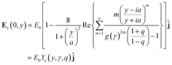 | (7) |
where a corresponds to the circle foci coordinate in bipolar coordinates,  ,
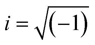
, 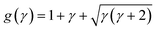 , which is a function of the gap-to-post ratio:and the ratio of material conductivities, q = σi/σo (σi for the inner dielectric and σo for the outer electrolyte). The subscript c has been used to designate the solution for the circular geometry. Notice that eqn (7), which is plotted in Fig. 2C, can be explicitly written as a product of the externally applied field E0ĵ, and a gain function encoding the amplification factor at y, which is independent of the DC-bias. Evaluation at the origin, where eqn (7) is maximum, results in:
| | 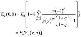 | (9) |
where the function Ψc corresponds to the DC field-independent amplification factor for the circular post geometry. This number indicates the fold increase in magnitude of the applied field E0ĵ provided the geometry (γ), and the ratio of conductivities (q).
Electric field solution for triangular posts.
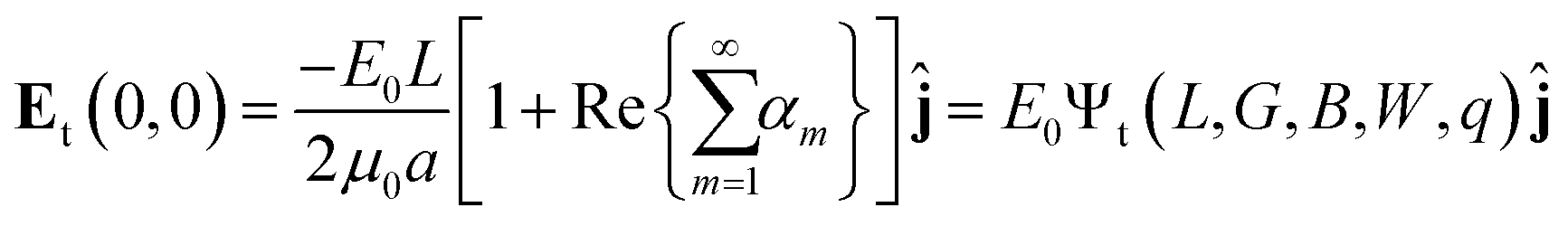
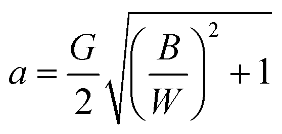
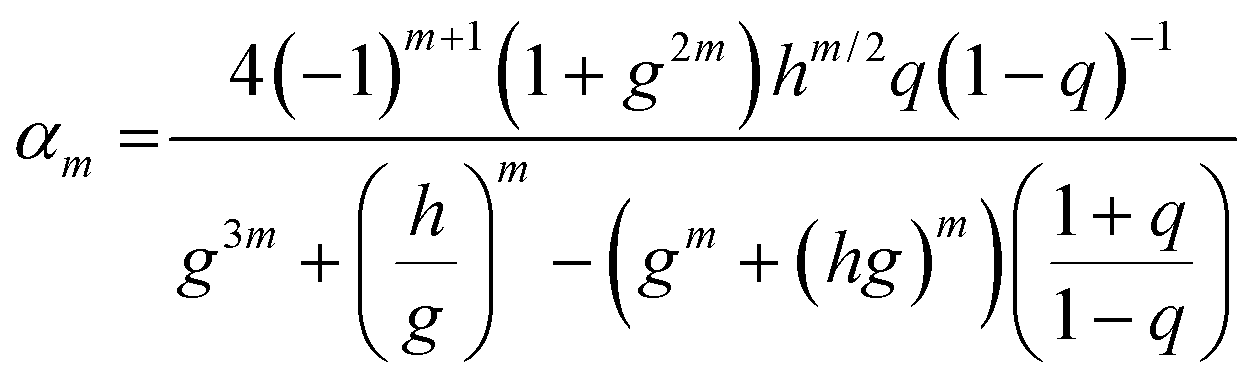
The above procedure can be generalized for other coordinate systems, provided that the boundary conditions can be suitably represented in those systems. We observed that a geometry consisting of a triangular dielectric constriction can be approximately represented by ν = constant curves (i.e., hyperbolas) in the elliptic system of coordinates (μ,ν) (see Fig. 2D). This representation has the added benefit of smoothing the triangular tips with a finite curvature radius (similar to what is observed in PDMS structures obtained by soft lithography30), instead of using unrealistically sharp tips. The foci of ellipses are located at (a,0) and (−a,0) in Cartesian coordinates, and can be related to the gap dimensions through the equation 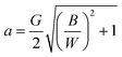 , where B is the base of the triangle post, and W the width of the microchannel (see ESI†). The solution to the Laplace equation in this coordinate system has been found by exploiting the symmetry of the boundary conditions, and by noting that the potential solution outside the dielectric (ϕo) requires that ϕo(ν,μ) = ϕo(π − ν,μ), and ϕo(ν,0) = 0 (see ESI† for the complete derivation). Evaluation of the applied field boundary condition leads to the 2D electric field solution in elliptic coordinates (Fig. 2E). In particular, the expression for the non-uniform electric field along the central axis of the channel is given by:
| | 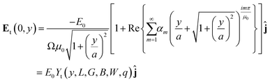 | (10) |
where the summation coefficients αm are:
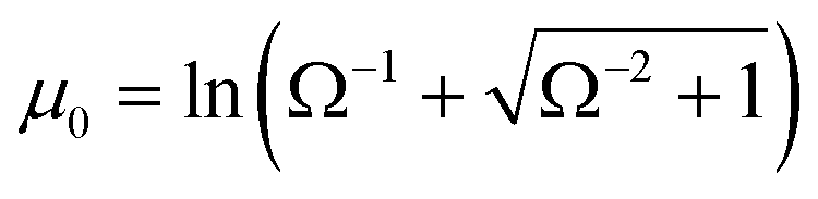
with the geometric functions g = exp(πν0μ−10), h = exp(π2μ−10), 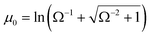 . Here, we have introduced the quantity:which denotes the ratio between the interfocal distance and the length of the device L. In eqn (10), the subscript t indicates the electric field solution for the triangular geometry. Furthermore, the value of the coordinate ν0 defining the dielectric/liquid interface corresponds to the angle between the x-axis and the hyperbola asymptote; thus ν0 = tan−1(B/W) (see Fig. 2D). As with the bipolar coordinate system, the maximum of eqn (10) occurs precisely at the origin, and therefore the electric field at (0,0) for the triangular post geometry is given by:
| | 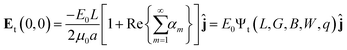 | (12) |
where again, the amplification Ψt(L, G, B, W, q) depends purely on the geometry and the ratio of conductivities, q.
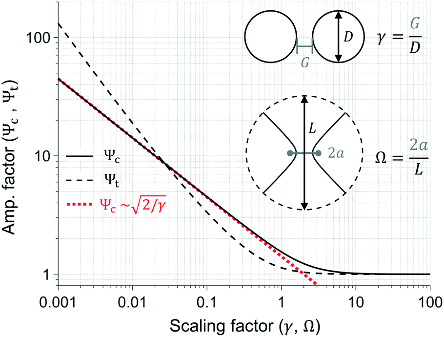
Electric field scaling laws.
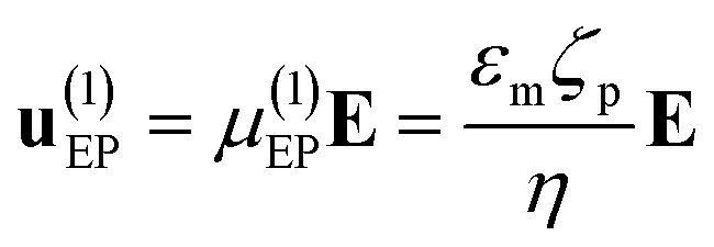
It must be emphasized that although eqn (7) and (10) are only solutions to geometries and boundary conditions that approximately represent the used microdevices, they capture the geometric scaling laws for the electric field non-uniformities in exact analytic expressions. Thus, the evaluation of eqn (9) and (12) for given geometries results in the amplification factor, which provides an estimate of the fold increase in electric field that can be expected when designing dielectric constrictions. Moreover, the amplification factor serves to quantitatively benchmark the trapping capabilities of each microdevice design. To illustrate the E field non-uniformity in the vicinity of the constriction, eqn (7) and (10) are plotted in Fig. 2C and F, where the device y-axis has been normalized to D and B, respectively, and where the E field has been normalized by the applied bias E0 to show the amplification obtained with these geometries.
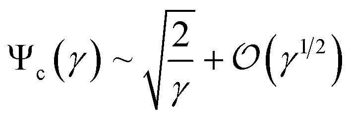
Inspection of eqn (9) and (12) shows that evaluating the parameters used in Table S2† yields the ideal case q = 0 (physically relevant when σi ≪ σo, such as in this work), resulting in the greatest amplification for a fixed geometry, and thus provides upper bounds for Ψc and Ψt. This simplification allows expressing eqn (9) and (12) as a function of the dimensionless ratios in eqn (8) and (11), respectively. Fig. 3 shows plots of the amplification factor of the two geometries as a function of the geometric scaling factors. In essence, these plots summarize the scaling laws of the E field magnitude and show two clear limits: i) when γ, Ω ≫ 1, constriction sizes become increasingly large and thus amplification effects vanish (Ψc, Ψt → 1); ii) when γ, Ω ≪ 1, gap sizes become smaller than the other relevant length scales in the system, which results in amplification factors growing exponentially as evinced by the constant slopes in the logarithmic plots of Fig. 3. Further analysis of eqn (9) for the upper bound case q = 0 and γ ≪ 1 allows approximating the indeterminate infinite series, evincing the scaling of the amplification factor as:
| |  | (13) |
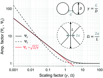 |
| | Fig. 3 Plot of the amplification factor for each geometry (bipolar or elliptic) as a function of the scaling factor (γ or Ω, respectively). Scaling factors are schematically indicated in the inset figures. Geometric quantities are not drawn to scale. | |
which was plotted in
Fig. 3 (see ESI
† for the derivation). For the elliptic coordinate system, evaluating
q = 0 in
eqn (12) leads to a closed form expression given by:
| |  | (14) |
which in contrast to
eqn (9) does not require an approximation, as no infinite series are involved when
q = 0. Insets in
Fig. 3 further illustrate how scaling factors
γ and Ω can be thought of as analogous quantities: when characteristic length scales
D and
L are fixed, the only way to increase the electric field magnitudes is to reduce interfocal distances. In the bipolar coordinate case, reducing
G intuitively changes this interfocal distance; for elliptic coordinates, since
G = 2
a![[thin space (1/6-em)]](https://www.rsc.org/images/entities/char_2009.gif)
cos
ν0, with 0 <
ν0 < π/2, one can reduce
G or alternatively decrease
ν0 to reduce 2
a (as seen in
Fig. 2D, lowering the angle
ν0 is equivalent to reducing the base of the triangle posts).
Experimental section
Computational model
A computational model was developed using COMSOL Multiphysics (COMSOL Inc. Burlington, MA, USA) to study the variation and scaling of the electric field under different post geometries. A 3D channel geometry with dimensions 1 cm long × 1 mm wide × 40 μm tall was used as an approximation of the fabricated devices—described in the microdevices section—to study the circular and triangular post designs. The amplification factors Ψc and Ψt from eqn (9) and (12) depend on the geometrical quantities γ = G/D and Ω = 2a/L, respectively. Therefore, a parametric study for the circular geometry was performed to optimize the post diameter (D) and the gap between the structures (G) with respect to the objective function Ψc; and for the triangular geometry, the study optimized the length of the triangle base (∼L) and the gap between structures (∼2a) with respect to the objective function Ψt. The numerically computed amplification factors, ΨNc and ΨNt, were extracted from a 10000 μm-long cutline at the center of the simulated channels between the insulating structures (see ESI† for a visualization of the cutline). Results from this model are discussed in the E field optimization section. Furthermore, a parametric sweep on the electric potential, which reproduces the voltage ramp applied in the experiments and described in the experimental procedures section, was used to study the mean velocity that a particle would experience when migrating across the channel. Particles have a velocity function described by eqn (6) that depends on the electric field distribution in the channel and will experience zero-velocity and get trapped at the EEEC. Results from this model are discussed in the trapping results section. ESI† Tables S1 and S2 lists the definitions and parameters employed in the COMSOL Multiphysics simulation.
Microdevices
Standard soft lithography techniques were used to fabricate microdevices by patterning the specific design in polydimethylsiloxane (PDMS) and completing the device by sealing the channel with a PDMS-coated glass wafer via plasma treatment of both contacting interfaces. The details of the process can be found elsewhere.31 This process ensured that all internal walls of the microchannel had the same wall zeta potential (ζW), resulting in consistent electroosmotic flow. For each design used, a mold to cast PDMS (Dow Corning, Midland, MI) was fabricated by spin coating the substrate with a 40 μm layer of SU-83050 photoresist (MicroChem, Newton MA) followed by soft baking at 95 °C for 15 min. After UV exposure of the photoresist to 225 mJ cm−2, baking was carried out at 95 °C for 11 min followed by development for 7 min and hard baking at 150 °C for 10 min. The dimensions of the 4 different microchannels designs used in this study are depicted in Fig. 1B.
Suspending medium and particle samples
The suspending media was DI water with adjusted pH and conductivity, by the addition of 0.1 M KOH and 0.05% (v/v) of Tween 20 (Amresco, New York, NY), to final values of pH = 6.0–6.5 and conductivity = 20–25 μS cm−1. Surfactant Tween 20 was added to prevent particle agglomeration. This suspending medium produced a wall zeta potential (ζW) of −97.3 mV and μEO = 7.58 × 10⁻⁸ m2 V−1 s−1 in the PDMS devices, as measured with current monitoring experiments.32 Two types of carboxylated polystyrene microparticles (Magsphere, Pasadena, CA) were used in this study and their characteristics are listed in Table 1. For experimentation, microsphere suspensions were diluted into the suspending media with concentrations of 7.2 × 10⁵ and 5. 7 × 10⁶ particles mL−1 for the 2 and 6.8 μm particles, respectively.
Table 1 Microparticle information and EK properties determined in this study
| Part. diameter [μm] |
Color |
ζ
p [mV] |
μ
(1)EP × 10−8 [m2 V−1 s−1] |
μ
(3)EP × 10−19 [m4 V−3 s−1] |
| 2 |
Red |
−57.5 |
−3.10 |
−8.97 |
| 6.8 |
Green |
−50.0 |
−2.70 |
−9.87 |
Experimental procedures.
All trapping experiments started with a clean microchannel that was conditioned by filling it with the suspending medium overnight. To decrease pressure driven backflow during the experiments, large reservoirs (∼2 mL) were placed at the inlet and outlet of the channel as shown in Fig. 1A. The particle suspension was then introduced in the reservoirs (2 and 1 μL, for the 2 and 6.8 μm particles, respectively). The particle concentration in the solution is small to avoid the formation of particle lumps and to achieve a high accuracy in the determination of the first trapping voltage for individual particles. Different particle suspension volumes were used for each particle size to have a comparable fluorescence level for the larger and smaller particles. This procedure was followed for testing channels shown in Fig. 1B. Particle separation experiments were performed in the same manner, with the difference that both types of particles were simultaneously introduced into the same channel. A “linear sweep” DC voltage was applied across the channel via a high voltage power supply (Model HVS6000D, LabSmith, Livermore, CA) fitted with platinum wire electrodes that were placed in the inlet and outlet reservoirs. Custom voltage sequences were created employing the software Sequence provided by the manufacturer of the voltage supply, increasing from 0 to 500 V at fixed increments of 4 V s−1 and from 0 to 250 V at fixed increments 2 V s−1 for the 2 and 6.8 μm particles, respectively. The mean standard deviation between the programmed and the experimental voltage sequences was of ±0.836 V. This voltage ramp at fixed increments allowed for a precise determination of the particle trapping value and was done at a higher interval for the 2 μm than the 6.8 μm because the smaller particle required on average 38% higher voltage values than the larger particle for achieving total trapping (i.e., when no particle can flow through the trapping region), and we decided to maintain the length of experiments the same for both particles. The voltage was varied systematically and the intensity of the collected fluorescently labeled particles was monitored as they accumulated near the constricted region (Movie S1†) and was recorded by time-lapse image sequences captured at 23.83 frames/s and 800 × 600 pixel resolution using a Leica DMi8 inverted microscope (Wetzlar, Germany) and a Zeiss Axiovert 40 CFL inverted microscope (Carl Zeiss Microscopy, Thornwood, NY). The fluorescence intensity data (background subtracted) near the constriction versus time (i.e., the applied voltage) were fitted into two segments, whose intersection point was taken as a variable optimized using the least squares method by a customized MATLAB R2018b (Mathworks Inc., Natick, MA) code. The applied voltage corresponding to the determined intersection point between the segments was extracted as the total trapping voltage and listed in Table 2. This enables an automatic and objective determination of the trapping voltage. All experiments were run in triplicate to ensure reproducibility.
Table 2 Total trapping voltage results for each of the channel and particle combinations
| Particle size [μm] |
Channel ID (as in Fig. 1B) |
Amp. factor (numerical) |
Fabricated gap [μm] |
Amp. factor (fabricated) |
First trap. [V] |
Total trap. [V] |
| 2 |
i |
25.64 |
25.1 ± 2.8 |
25.0 ± 2.7 |
169.3 ± 10.1 |
213.0 ± 46.2 |
| 2 |
ii |
50.73 |
14.5 ± 0.1 |
42.0 ± 0.3 |
163.3 ± 12.1 |
190.7 ± 18.0 |
| 2 |
iii |
59.9 |
14.7 ± 5.7 |
45.8 ± 18.2 |
128.7 ± 5.0 |
158.7 ± 11.5 |
| 6.8 |
i |
25.64 |
25.1 ± 2.8 |
25.0 ± 2.7 |
154.7 ± 14.2 |
190.0 ± 9.2 |
| 6.8 |
ii |
50.73 |
14.5 ± 0.1 |
42.0 ± 0.3 |
88.7 ± 4.6 |
92.0 ± 3.5 |
| 6.8 |
iii |
59.9 |
14.7 ± 5.7 |
45.8 ± 18.2 |
82.0 ± 10.3 |
80.3 ± 14.5 |
Results and discussion
E-field optimization
Eqn (13) and (14), obtained in the theoretical analysis of the electric field scaling laws, allowed us to draw important conclusions about the impact of geometry: i) amplification is directly dependent on the relative magnitudes of two relevant length scales—one capturing the scale of the constriction, and the other reflecting the size of the post; ii) for a fixed constriction size, which is typically the limiting design parameter, the amplification factor can be increased by enlarging the remaining length scale parameter relative to the constriction size; and iii) the amplification factor in geometries with sharper posts scale more favorably, as evinced by the slope differences in Fig. 3, as well as by visual inspection of the electric field distributions in Fig. 2Cvs.Fig. 2F (Ψc ∼ 7 and Ψt ∼ 65 for the circular and triangular geometries, respectively, of equal gap and diameter/triangle base). Building on these theoretical results, we carried out 3D finite element simulations of the microchannels optimizing for the two parameters/length scales, since the addition of a bounding rectangular microchannel evidently admits no analytical calculations of the complete geometry. We have therefore parametrically analyzed the effects of the following quantities on the amplification factor: gap size (G) and diameter (D) in the circular geometry case; gap size (G) and triangle base (B), in the triangular geometry.
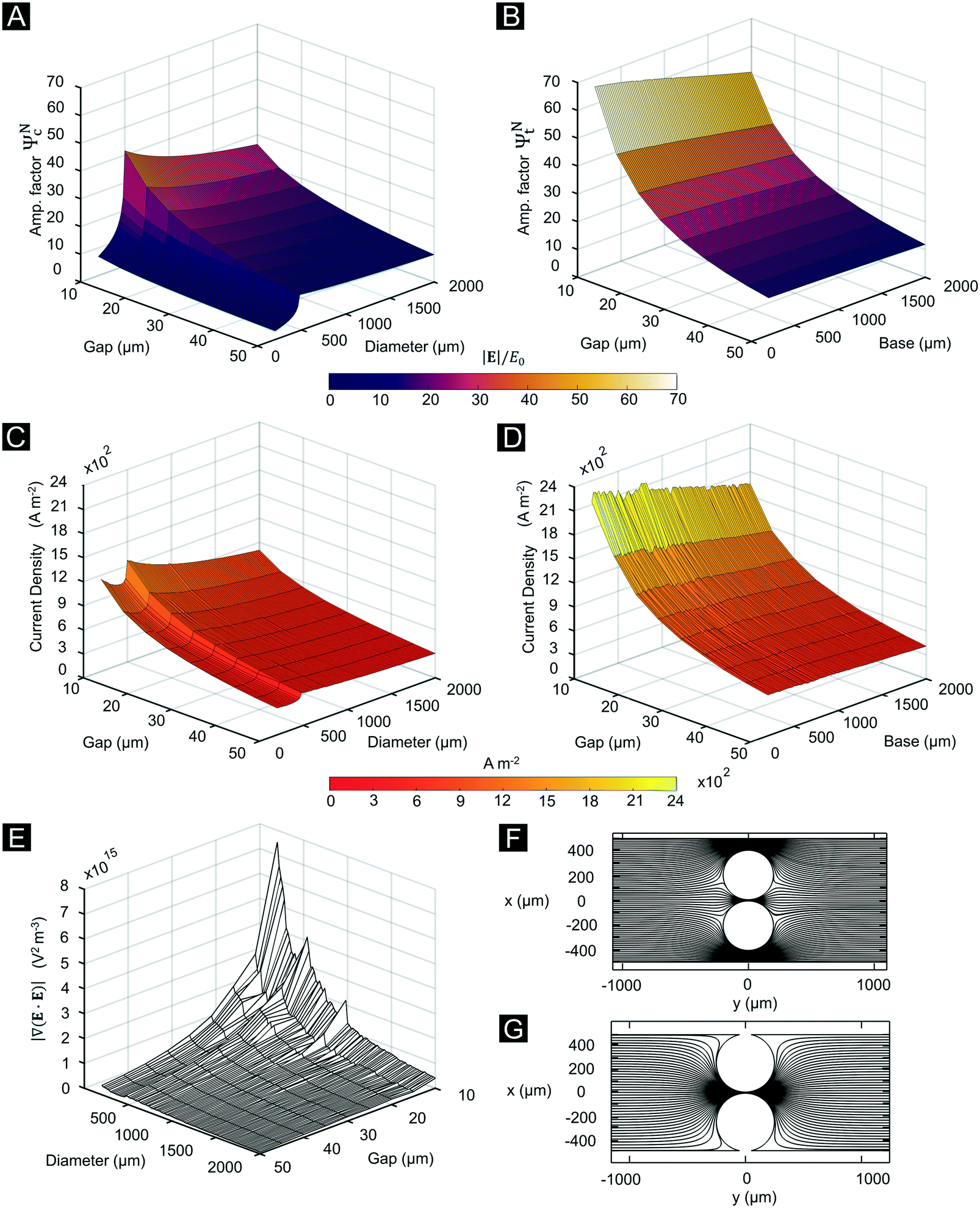
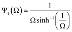
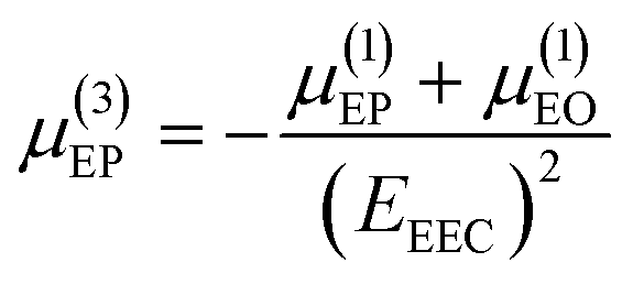
Surface plots of the numerically computed amplification factors (ΨNc and ΨNt) as a function of design parameters shown in Fig. 4A and B, which were obtained by extracting the amplification factor at y = 0 for both 3D geometries (corresponding to the maximum amplification along a 10000 μm cutline in our simulation, see Fig. S2†). Maximum values for ΨNc and ΨNt were 25.64 and 59.9, respectively obtained for the minimum gap size studied of 10 μm—results that agree with the intuitive notion that gap size reduction yields the strongest E field. The 10 μm minimum gap size was selected as it was the minimum feature size achievable by our micro-fabrication process. Furthermore, the circular geometry reached the greatest ΨNc value for a post diameter of 500 μm, while the triangular geometry reached the greatest ΨNt when the length of the triangle base was minimum in size.
 |
| | Fig. 4 Computational modelling results from the parametric study for the circular and triangular geometries. (A) ΨNc as a function of the optimized variables for the circular geometry. (C) Electric current density ∣J∣ as a function of optimized variables for the circular geometry. (B and D) In analogy to (A and C), figures are displayed for the triangular geometry. (E) ∣∇(E·E)∣ as a function of optimized variables for the circular geometry. Electric field lines for two circular geometries: (F) non-optimal geometry with small posts and (G) optimal geometry with posts touching the channel walls. | |
We further found that confinement of posts within the rectangular microchannel had a counterintuitive effect not predicted by the theoretical models in the case of the circular geometry. Because electric field lines can either go inside the gap formed by the circular posts, or surround them from the outer side, there will be an effect when the rectangular walls are close to the posts. Thus, instead of indefinitely increasing the amplification factor as suggested by eqn (13) for a fixed gap size, we see a reduction beyond ∼500 μm post diameters in Fig. 4A. Evidently, posts of larger diameter cannot be fitted inside the rectangular channel, and therefore this corresponds to the point at which all electric field lines go inside the gap and contribute to the amplification. Conversely, in the triangular geometry case, the situation does not arise because all lines pass through the constriction region.
Next, we show that the electric field enhancement can be intuitively and quantitatively described in terms of the electric current density within the constriction. Because the magnitude of the electric current density at the gap region can be defined as |J| = σo|E|, we can expect that the configurations that maximize this quantity will result in the highest amplification factors (see ESI† section 2.1 for an explanation on its computation). As seen in Fig. 4C, the value of |J| accurately captures the optimization trends shown in Fig. 4A, where the optimal configuration for the circular structures occurs with posts 500 μm in diameter and 10 μm in gap size. Similarly, in Fig. 4D the value of |J| reflects the optimization trends in Fig. 4B, where the optimal configuration for the triangular structures occurs when the length of the base of the triangular structures and the gap are minimum in size.
Our numerical results demonstrated that optimizing for the maximum amplification factor enhancement does not necessarily lead to the same optimized geometry obtained if |∇(E·E)| was maximized instead. This counterintuitive result was verified by computing the average of |∇(E·E)| over the constriction area in the circular geometry (Fig. 4E), which leads to the conclusion that the optimized geometry is the case G: 10 μm, D: 200 μm. That geometry, however, results in |J| = 13.54 × 10² A m−2, which is lower than the current density obtained for the G: 10 μm, D: 500 μm case that optimizes the amplification factor (|J| = 14.92 × 10² A m−2). Fig. 4F shows the former case, where only 11% of electric field lines enter the central constriction area, resulting in ΨNc = 7.07, whereas the optimal case in Fig. 4G amplifies up to ΨNc = 25.64 with 100% of the lines concentrated in the gap. Similarly, we computed |J| for the non-optimal triangular channel geometry shown in Fig. 1B, ii (19.39 × 10² A m−2 and ΨNt = 50.73) as well as for the optimal triangular channel shown in Fig. 1B, iii (23.34 × 10² A m−2 and ΨNt = 59.9). Therefore, the presented theoretical and numerical study illustrates that electric current density optimization leads to the greatest amplification factor enhancement, which is the decisive factor (rather than the distribution of ∇(E·E)) in particle trapping voltage, as recently suggested by observations on DC-iEK devices.6
Particle trapping results
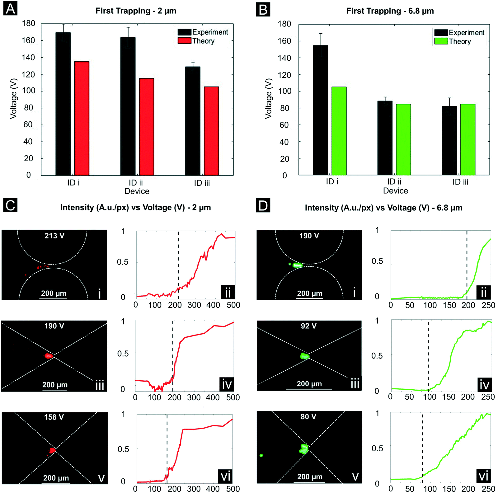
We tested the particle trapping performance of the fabricated microdevices (Fig. 1) to determine the “first trapping” and “total trapping” voltages. Here, the first trapping voltage is defined as the applied potential difference at which particles begin to trap (i.e., when there is a balance of the linear EO and EP phenomena and higher order effects of EP(3) for the buffer−particle−electric field system) at the gap between posts while other particles keep flowing through. Total trapping, on the other hand, occurs when the applied potential difference is high enough so that no particle can cross the gap between posts. The first trapping results are shown in Table 2, along with measurements of the device gaps and calculated amplification factors for those geometries. We show in this table an inverse relationship between calculated amplification factors and the first trapping voltages, which can be explained by means of eqn (6). Using this equation, in combination with the EK properties of Table 1, allowed us to determine the theoretical electric field magnitude—and hence, voltage—at which particles halt (i.e., zero velocity). Fig. 5A and B depict bar plots comparing this prediction and the experimental first trapping voltages. The average relative error between the experimental and theoretical trapping for all cases is 18.02% with the relative error for the ideal geometry (ID iii) being of only 3.66% (our prediction used no correction factor to compensate for an order of magnitude mismatch, as opposed to previous studies).33 The measured fluorescence intensity increased with time as higher voltages were applied and particles began to trap, this is shown in Fig. 5C and D. A segmented regression routine optimized using the least squares method was implemented to quantify the experimental fluorescence intensity and obtain an automatic and objective determination of trapping voltages (see ESI† Video S1 for a demonstration). The nonlinear EP(3) mobility for the 6.8 μm particle is 10% larger than the one for the 2 μm particle. This explains the observation of 6.8 μm particles being trapped at lower voltages than the 2 μm particles.
 |
| | Fig. 5 Trapping voltages for different device and particle combinations. (A) First trapping voltage for the 2.0 μm particle. The bars in gray color show the first trapping voltage observed experimentally, the bars in red color show the first trapping voltages computed using eqn (6) (C i, iii, v) Total trapping voltage for device ID i, ID ii, and ID iii respectively (C ii, iv, vi) fluorescence intensity plotted as the applied voltage is increased until total trapping is achieved (B and D) in analogy to (A and C) figures are displayed in green for the 6.8 μm particle. | |
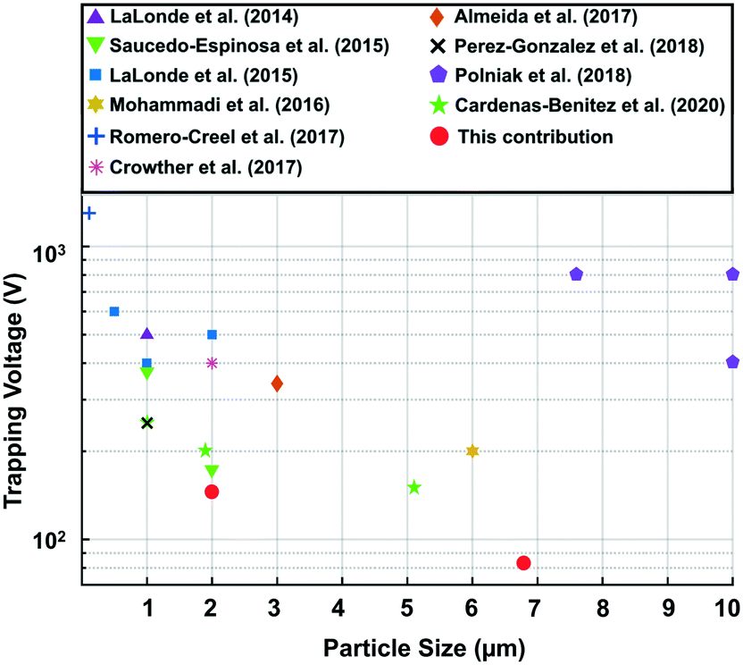
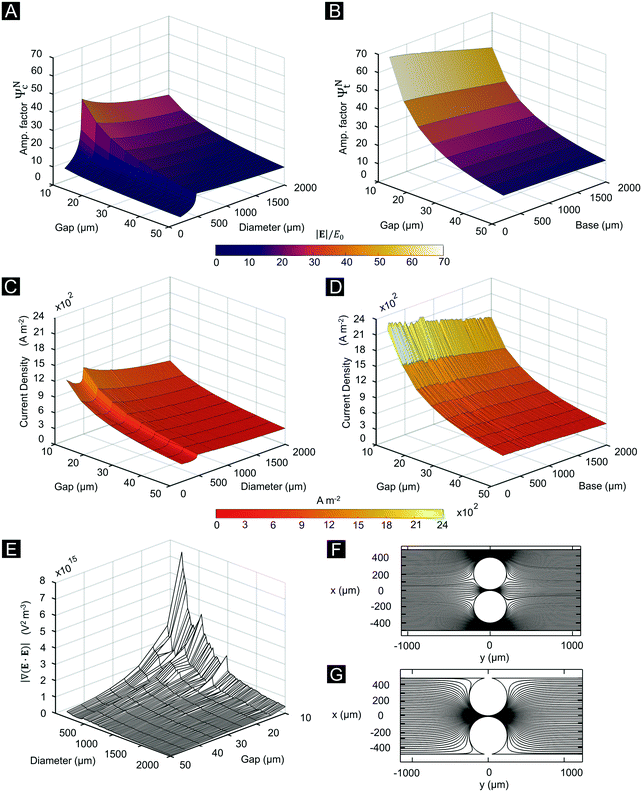
Table 2 summarizes the results and shows that lower applied voltages are required for particle trapping as the amplification factor of the channel geometry is increased. Additionally, the total trapping voltage range is wide, varying from 158.7 to 213.3 V for the 2 μm particle and from 80.3 to 190.0 V for the 6.8 μm particle; this corresponds to a reduction in the trapping voltage between the channel with the lowest and highest amplification factor of 25% and 58% for the 2 μm and the 6.8 μm particles, respectively. Fig. 6 shows a comparative chart of the particle diameter versus trapping voltages reported in the literature, including the results here obtained. Works that focused on polystyrene particle trapping with DC-iEK devices have been selected to provide a fair comparison. Although different media were tested across studies, our results confirm that values of ∼80 V can be attained at the standard conductivity of 20–25 μS cm−1 being the lowest trapping voltages reported to date for these particle size ranges. Moreover, our trapping voltages for 2 μm particles were found to be half an order of magnitude lower than the voltages employed in other works, while 6.8 μm particles were trapped at 1 order of magnitude lower voltages in comparison to previous studies. We further tested our two particle solutions for trapping in a non-optimized, multi-column microchannel with typical dimensions found in the literature as a control (Fig. 1B, iv). However, no trapping was observed for this channel for the complete voltage sweep, confirming the hypothesis that multi-column devices increase voltage requirements to excessively high values,24 since increasing the number of columns decreases the |J| and the amplification factor.
 |
| | Fig. 6 Scatter plot comparing trapping voltage for different polystyrene particle size from previous works on insulator-based devices6,18–24 and this contribution. | |
Although nonlinear electroosmotic vortex flows have been observed near dielectric tips in high conductivity mediums stimulated with AC fields,34 it is implausible for this phenomenon to be significant in the present study given that the medium had a low conductivity and was stimulated with DC fields.
Application: enabling the iEK separation of microparticles
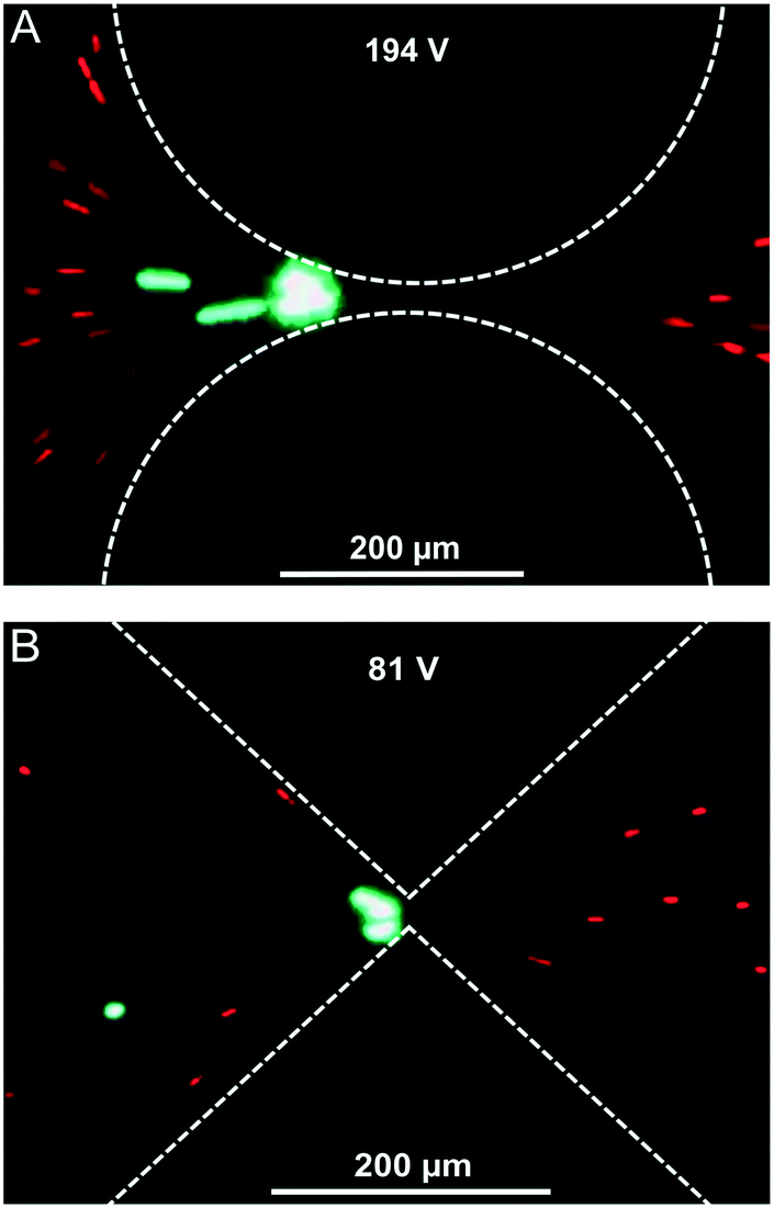
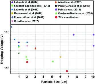
We used our optimized microchannels to test the separation of the 2 μm and 6.8 μm particles (Fig. 1B, i and iii devices, respectively). Fig. 7A and B depict the results demonstrating that total particle trapping can be achieved for both circular and triangular post geometries at 194 V and 81 V, respectively. These results are consistent with the total trapping achieved for each individual particle as shown in Table 2. Furthermore, the decrease in voltage requirements is significant as particle separation in Fig. 7B was achieved employing only 4% of the voltage reported in similar systems, where particle trapping occurred at ∼3000 V.14–16 These results are encouraging, as they show that the electrokinetic trapping of similar microparticles is now possible at much lower applied voltages than previously reported.18–24 By simply optimizing the system design to maximize the electric current density along the constriction, the particle trapping capabilities of the system are enhanced while voltage requirements are reduced, enabling the trapping and detection of valuable microparticles.
 |
| | Fig. 7 Separation of a 6.8 μm (green) and 2 μm (red) particle mixture. (A) A separation of the mixture using a device with circular geometry, separation was achieved at 194 V. (B) Separation of the mixture using a device with triangular geometry, separation was achieved at 81 V. | |
Conclusion
The dielectric constrictions here explored (circular and triangular) generally have two main geometric degrees of freedom, each of which impacts the magnitude of the attainable amplification factor. Interestingly, for the theoretical case of q = 0 (i.e., σi ≪ σo), the two degrees can be reduced to a single scaling parameter (gap-to-post ratio, γ, and the interfocal distance-to-length ratio, Ω), evincing that it is the relative magnitude between these amounts, which ultimately impacts the scaling of the amplification. By exploring the design variables in the complete 3D microchannel, we found through finite element simulations that confinement of dielectric posts within the rectangular channel housing affects the electric current density distribution (|J|) at the constriction, which in turn dictates the fold-increase in the E field. These simulations also allowed us to estimate optimal amplification factors and subsequently predict particle trapping by means of applying the non-linear EK theory involving EP(3) velocities, rather than dielectrophoretic velocities (∼∇(E·E)). In doing so, we have shown that EP mobilities not only provide good estimates of the trapping voltages (average relative error 18.02%), but also experimentally demonstrated that optimization should prioritize increasing |E| (as higher amplification factors led to lower trapping voltages). Most importantly, the complete methodology resulted in ∼80 V total trapping voltages for 6.8 μm particles in the triangular post device, which are, to our knowledge, the lowest values reported for those using DC-iEK devices fabricated by single layer soft-lithography. We anticipate that building microdevices with features that closely resemble the theoretical geometries in the limit of small scaling factors (Fig. 3) will further maximize the attainable amplifications—thus allowing for increasingly lower voltages amenable to lab-on-a-chip systems.
Author contributions
Rodrigo Ruz-Cuen: methodology, formal analysis, data curation, software, writing – original draft, review and editing, and visualization. J. Martin de los Santos-Ramirez: methodology, formal analysis, data curation, writing – original draft, review and editing, and visualization. Braulio Cardenas-Benitez: methodology, formal analysis, data curation, writing – original draft, review and editing, and visualization. Cinthia J. Ramirez-Murillo: methodology, data curation, review and editing. Abbi Miller: investigation and validation. Kel Hakim: investigation and validation. Blanca H. Lapizco-Encinas: methodology, resources, writing – review and editing. Victor H. Perez-Gonzalez: conceptualization, methodology, formal analysis, supervision, project administration, writing – review and editing.
Conflicts of interest
There are no conflicts to declare.
Acknowledgements
The authors would like to acknowledge the financial support provided by the National Science Foundation (Award CBET-1705895), and by Tecnologico de Monterrey through the Nano- Sensors & Devices Research Group (0020209I06) and the Federico Baur Endowed Chair in Nanotechnology (0020240I03). VHPG and JMdlSR also acknowledge the financial support provided by the Consejo Nacional de Ciencia y Tecnología (SNI Grant 62382 and Ph.D. Fellowship Grant 786664, respectively).
Notes and references
- W. Su, X. Gao, L. Jiang and J. Qin, J. Chromatogr. A, 2015, 1377, 13–26 CrossRef CAS PubMed.
- B. H. Lapizco-Encinas, Electrophoresis, 2019, 40(3), 358–375 CrossRef CAS PubMed.
- V. H. Perez-Gonzalez, Electrophoresis, 2021 DOI:10.1002/elps.202100123 , in press.
- V. Shilov, S. Barany, C. Grosse and O. Shramko, Adv. Colloid Interface Sci., 2003, 104, 159–173 CrossRef CAS PubMed.
- S. S. Dukhin, Adv. Colloid Interface Sci., 1991, 35, 173–196 CrossRef CAS.
- B. Cardenas-Benitez, B. Jind, R. C. Gallo-Villanueva, S. O. Martinez-Chapa, B. H. Lapizco-Encinas and V. H. Perez-Gonzalez, Anal. Chem., 2020, 92, 12871–12879 CrossRef CAS PubMed.
- A. Coll De Peña, A. Miller, C. J. Lentz, N. Hill, A. Parthasarathy, A. O. Hudson and B. H. Lapizco-Encinas, Anal. Bioanal. Chem., 2020, 402, 3935–3945 CrossRef PubMed.
- S. Antunez-Vela, V. H. Perez-Gonzalez, A. Coll De Pena, C. J. Lentz and B. H. Lapizco-Encinas, Anal. Chem., 2020, 92(22), 14885–14891 CrossRef CAS PubMed.
- A. Coll De Peña, N. Hill and B. H. Lapizco-Encinas, Biosensors, 2020, 10, 148 CrossRef PubMed.
- G. R. Pesch, F. Du, M. Baune and J. Thöming, J. Chromatogr. A, 2017, 1483, 127–137 CrossRef CAS PubMed.
- D. Kim, M. Sonker and A. Ros, Anal. Chem., 2019, 91, 277–295 CrossRef CAS PubMed.
- X. Xuan, Electrophoresis, 2019, 40, 2484–2513 CAS.
- A. Rohani, J. H. Moore, J. A. Kashatus, H. Sesaki, D. F. Kashatus and N. S. Swami, Anal. Chem., 2017, 89, 5757–5764 CrossRef CAS PubMed.
- M. F. Romero-Creel, E. Goodrich, D. V. Polniak and B. H. Lapizco-Encinas, Micromachines, 2017, 8, 239–253 CrossRef PubMed.
- M. A. Mata-Gomez, V. H. Perez-Gonzalez, R. C. Gallo-Villanueva, J. Gonzalez-Valdez, M. Rito-Palomares and S. O. Martinez-Chapa, Biomicrofluidics, 2016, 10, 033106 CrossRef PubMed.
- M. A. Saucedo-Espinosa, A. LaLonde and A. Gencoglu, Electrophoresis, 2016, 37, 282–290 CrossRef CAS PubMed.
- R. C. Gallo-Villanueva, V. H. Perez-Gonzalez, B. Cardenas-Benitez, B. Jind, S. O. Martinez-Chapa and B. H. Lapizco-Encinas, Electrophoresis, 2019, 40, 1408–1416 CrossRef CAS PubMed.
- W. A. Braff, A. Pignier and C. R. Buie, Lab Chip, 2012, 12, 1327–1331 RSC.
- C. V. Crowther and M. A. Hayes, Analyst, 2017, 142, 1608–1618 RSC.
- G. R. Pesch, L. Kiewidt, F. Du, M. Baune and J. Thöming, Electrophoresis, 2016, 37, 291–301 CrossRef CAS PubMed.
- J. S. Kwon, J. S. Maeng, M. S. Chun and S. Song, Microfluid. Nanofluid., 2008, 5, 23–31 CrossRef CAS.
- A. LaLonde, A. Gencoglu, M. F. Romero-Creel, K. S. Koppula and B. H. Lapizco-Encinas, J. Chromatogr. A, 2014, 1344, 99–108 CrossRef CAS PubMed.
- M. A. Saucedo-Espinosa and B. H. Lapizco-Encinas, J. Chromatogr. A, 2015, 1422, 325–333 CrossRef CAS PubMed.
- V. H. Perez-Gonzalez, R. C. Gallo-Villanueva, B. Cardenas-Benitez, S. O. Martinez-Chapa and B. H. Lapizco-Encinas, Anal. Chem., 2018, 90, 4310–4315 CrossRef CAS PubMed.
- Q. Chen and Y. J. Yuan, RSC Adv., 2019, 9, 4963–4981 RSC.
- C. J. Ramirez-Murillo, J. M. de los Santos-Ramirez and V. H. Perez-Gonzalez, Electrophoresis, 2021, 42, 565–587 CrossRef CAS PubMed.
-
B. J. Kirby, Micro-and nanoscale fluid mechanics: transport in microfluidic devices, Cambridge university press, 2010 Search PubMed.
- O. Schnitzer, R. Zeyde, I. Yavneh and E. Yariv, Phys. Fluids, 2013, 25, 052004 CrossRef.
- O. Schnitzer and E. Yariv, Phys. Fluids, 2014, 26, 122002 CrossRef.
- T. W. Odom, J. C. Love, D. B. Wolfe, K. E. Paul and G. M. Whitesides, Langmuir, 2002, 18(13), 5314–5320 CrossRef CAS.
- D. V. Polniak, E. Goodrich, N. Hill and B. H. Lapizco-Encinas, J. Chromatogr. A, 2018, 1545, 84–92 CrossRef CAS PubMed.
- M. A. Saucedo-Espinosa and B. H. Lapizco-Encinas, Biomicrofluidics, 2016, 10, 033104 CrossRef PubMed.
- N. Hill and B. H. Lapizco-Encinas, Electrophoresis, 2019, 40(18–19), 2541–2552 CAS.
- Y. Ren, W. Liu, Y. Tao, M. Hui and Q. Wu, Micromachines, 2018, 9, 102 CrossRef PubMed.
Footnote |
| † Electronic supplementary information (ESI) available. See DOI: 10.1039/d1lc00614b |
|
| This journal is © The Royal Society of Chemistry 2021 |

 Open Access Article
 This Open Access Article is licensed under a Creative Commons Attribution-Non Commercial 3.0 Unported Licence
 a,
Braulio
Cardenas-Benitez
b,
Cinthia J.
Ramírez-Murillo
a,
Abbi
Miller
c,
Kel
Hakim
c,
Blanca H.
Lapizco-Encinas
a,
Braulio
Cardenas-Benitez
b,
Cinthia J.
Ramírez-Murillo
a,
Abbi
Miller
c,
Kel
Hakim
c,
Blanca H.
Lapizco-Encinas

 ,
,  , which is a function of the gap-to-post ratio:
 , where B is the base of the triangle post, and W the width of the microchannel (see ESI†). The solution to the Laplace equation in this coordinate system has been found by exploiting the symmetry of the boundary conditions, and by noting that the potential solution outside the dielectric (ϕo) requires that ϕo(ν,μ) = ϕo(π − ν,μ), and ϕo(ν,0) = 0 (see ESI† for the complete derivation). Evaluation of the applied field boundary condition leads to the 2D electric field solution in elliptic coordinates (Fig. 2E). In particular, the expression for the non-uniform electric field along the central axis of the channel is given by:
 . Here, we have introduced the quantity: